ACPL-0820
High Current Dual Line-Driver IC
Data Sheet
Lead (Pb) Free
RoHS 6 fully
compliant
RoHS 6 fully compliant options available;
-xxxE denotes a lead-free product
Description
Features
ACPL-0820 is a high current dual line-driver IC. With a 5 V
single supply, it delivers up to 1.5 APP current. This is ideal
for high current differential mode applications such as a
Powerline modem.
•
•
•
•
•
ACPL-0820 is internally protected against over-temperature conditions through thermal shutdown and this status
is reported by the Status pin. Over-load condition is sensed
by internal detection circuitry and is also reported by the
Status pin. In addition, with the transmit enable (Tx-en) input, the line-driver output stage can be disabled to reduce
power dissipation when not operating.
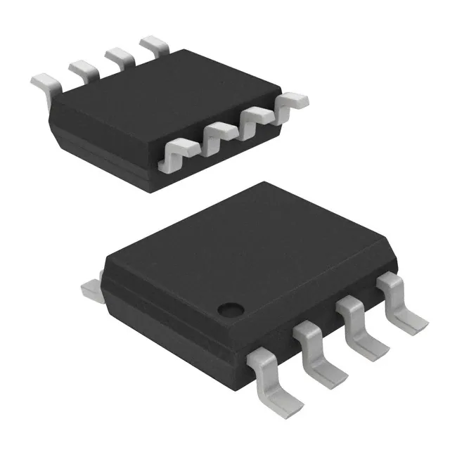
ACPL-0820 is designated for operation over extended temperature range from -40°C to +85°C. ACPL-0820 is available
in SO-8 package.
Applications
•
•
•
•
•
Automatic meter reading (AMR)
Powerline modem
General purpose line driver
Signal conditioning
Digital-to-analog converter buffers
•
•
•
•
•
•
Dual Line-Drivers
1.5 APP driving current
3 MHz gain bandwidth product
-60 dB maximum harmonic distortion
Drives 7Ω load under bridge configuration
with low distortion
Differential or Single ended to differential
connections
Load detection function
Over-temperature shutdown
5 V single supply
Temperature range: -40°C to +85°C
Suitable for FCC Part 15 and EN50065-1
compliant design
�Connection Diagrams
a) Differential to differential Connections
R3
5V
1
STATUS
TXp
Filter
TXn
R1
2
Vin R2
3
Status
4
TX-EN
Vdd
In1
Out1
In2
Out2
Tx -en
Gnd
ACPL-0820
PLM Transceiver
Gain of Amp1 = - R3/R1,
8
L
5V
7
Vout
6
5
N
R4
R1=R2, R3=R4, Overall Differential Output V out = (R3/R1) . V in
Gain of Amp2 = - R4/R2,
b) Single-ended to single-ended Connections
5V
1
STATUS
2
TX
Vin R1
Filter
3
4
TX -EN
Status
Vdd
In1
Out1
In2
Out2
Tx -en
PLM Transceiver
Gnd
8
L
5V
7
6
Vout
5
N
ACPL -0820
R2
Gain of Amp2 = - R2/R1, Overall Output Voltage Vout = - (R2/R1)
.V
in
c) High Driving Capacity Connections of Dual Line Drivers
5V
R2
I out
1
STATUS
Vin
TX
TX-EN
PLM Transceiver
Filter
R1
R3
2
3
4
Status
In1
Vdd
Out1
Out2
In2
Tx -en
ACPL-0820
Gnd
8
5V
L
I out1
7
1Ω
>1µF
6
1Ω
>1µF
5
Vout
I out2
R4
Gain of Amp1 = - R2/R1, Gain of Amp2 = - R4/R3, R1 = R3, R2 = R4, R5 = R6, Overall Output Voltage Vout ≈ - (R2/R1) . Vin, Iout = Iout1+Iout2
�
N
�Package Pin Out
Pin Descriptions
Vdd
1 Status
8
2 In1
Out1
7
3 In2
Out2
6
4 Tx -en
Gnd 5
Pin No.
Symbol
Function
Description
1
Status
Line condition detection
A logic low indicates line conditions such as
- load detection for Iout < -0.25 A- over-temperature detection for Tj =130°C (typ.)
2
In1
Amp1 Input
Transmit signal input for 1st Line Driver
3
In2
Amp2 Input
Transmit signal input for 2nd Line Driver
4
Tx-en
Transmit enable
A logic high enables both outputs (Out1 & Out2)
of the dual line drivers;A logic low disables both
outputs and setit to high impedance state (tristate)
5
GND
Power supply ground
Power supply and signal ground
6
Out2
Amp2 output
Transmit signal output for 2nd Line Driver
7
Out1
Amp1 output
Transmit signal output for 1st Line Driver
8
VDD
5 V power supply
5 V DC power supply
Block Diagram
Status
1
8
Vdd
Amp1
+
In1
2
V REF (2.25V)
3
Out1
6
Out2
Over -Temp
Detection
Status
Output
In2
7
Load
Detection
V REF (2.25V)
+
Amp2
-
Tx -en
�
4
5
Gnd
�Ordering Information
Option
Part number
RoHS Compliant
Packaging
Surface Mount
ACPL-0820
-000E
SO-8
X
-500E
SO-8
X
Tape & Reel
Quantity
100 per tube
X
1500 per reel
To order, choose a part number from the part number column and combine with the desired option from the option
column to form an order entry.
Example 1:
ACPL-0820-500E to order product of SO-8 package in Tape and Reel packaging and RoHS compliant.
Option datasheets are available. Contact your Avago sales representative or authorized distributor for information.
Remarks: The notation ‘#XXX’ is used for existing products, while (new) products launched since 15th July 2001 and RoHS
compliant option will use ‘-XXXE‘.
Package Outline Drawings
ACPL-0820 Small Outline SO-8 Package
DIMENSIONS IN INCHES AND (MILLIMETERS)
�
�Recommended Pb-free IR Profile
30 seconds
Temperature (°C)
250°C
260°C (Peak Temperature)
217°C
200°C
150°C
25°C
60 sec
60 ~ 150 sec
90 sec
1) One-time soldering reflow is recommended
within the condition of temperature and time
profile shown.
2) When using another soldering method such
as infrared ray lamp, the temperature may
rise partially in the mold of thedevice. Keep
the temperature on the package of the device
within the condition of (1) above.
60 sec
Time (sec)
Note: Non-halide flux should be used.
Absolute Maximum Ratings
Parameter
Symbol
Min.
Max.
Unit
Storage Temperature
TS
-55
125
°C
Ambient Operating Temperature
TA
-40
85
°C
Junction Temperature
TJ
150
°C
Supply Voltage
VDD
-0.5
5.5
Volts
Output Voltage
VO
-0.5
VDD
Volts
Tx-in Voltage
VIN1 or VIN2
-0.5
VDD
Volts
Tx-en Voltage
V Tx-en
-0.5
VDD
Volts
Solder Reflow Temperature Profile
(See Solder Reflow Temperature Profile Section)
Recommended Operating Conditions
Parameter
Symbol
Min.
Typ.
Max.
Unit
Ambient Operating Temperature
TA
-40
25
85
°C
Supply Voltage
VDD
4.75
5
5.25
V
�
�Electrical Specifications
Unless otherwise noted, for sinusoidal waveform input, all typical values are at TA = 25°C and VDD = 5 V; all Minimum/
Maximum specifications are at Recommended Operating Limits. (Note: VIn = VIn1 - VIn2)
Parameter
Symbol
VDD Supply Current
Idd
Min.
Typ.
Max.
Unit
Test Condition
Fig.
2.1
7.1
mA
1
30
40
mA
Status Logic High Output
VStatus-H
VDD-1
VDD
V
V Tx-en = 0V, VInp (& VInn )= 0VPP,
IOut (IOut1 & IOut2) no load
V Tx-en = 5V, VInp (& VInn )= 0VPP,
IOut (IOut1 & IOut2) no load
V Tx-en = 5V, VInp (or VInn )=
0VPP,IOut (IOut1 & IOut2) no load
V Tx-en = 5V, VInp (or VInn )= 1VPP,
IOut (IOut1 & IOut2) no load
V Tx-en = 5V, VInp (& VInn )=
1.25VPP,f=132kHz, Gain = -2,
RL1 (&RL2) = 2.5W
VDD = 3.5V, IStatus = -2mA
Status Logic Low Output
VStatus-L
0
0.8
V
VDD = 5V, IStatus = 2mA
Power SupplyRejection Ratio
PSRR
72
dB
DC Bias Voltage
VBias
2.25
V
Output Impedance
ZO
12
kW
0.5
W
3
MHz
Junction Over-Temperature
Detection Threshold
Junction Over-Temperature
Shutdown Threshold
Load Detection Threshold
130
°C
150
°C
0.5
(Diff )
App
2nd Harmonic Distortion
HD2
-69
-60
dB
3rd Harmonic Distortion
HD3
-74
-65
dB
50Hz ripple, Vrippe 200mVPP,
V Tx-en = 5V, VInp (or VInn )= 0VPP,
IOut (IOut1 & IOut2) no load
V Tx-en = 5V,
IOut (IOut1 & IOut2) no load
V Tx-en = 0V, VInp (or VInn )= 0VPP,
open loop, f =132kHz
V Tx-en = 5V, VInp (or VIn2 )= 0VPP,
f =132kHz
V Tx-en = 5V, VIn1 (or VInn)= 1VPP,
RL1 (&RL2) = 25W
VInp (or VInn )= 1VPP, f =132kHz,
IOut (IOut1 & IOut2) no load
V Tx-en = 0->5V, VInp = 1.25VPP,
VInn = 3.25VPP, f =132kHz,
RL1 (&RL2) = 470W
V Tx-en = 5->0V, VInp = 1.25VPP,
VInn = 3.25VPP, f =132kHz,
RL1 (&RL2) = 470W
V Tx-en = 5V,
VOut1 (& VOut2)= 3.5VPP,
Gain = -2, RL = 50WTA=25°C
Output Current
IO
1.5
APP
V Tx-en = 5V, f= 132kHz
Thermal Resistance
qJA
110
°C/W 1oz. copper trace, 2-layer PCB,
still air, TA=25°C
°C/W 1oz. copper trace, 4-layer PCB,
still air, TA=25°C
dB
V Tx-en = 5V,
VOut1 (& VOut2)= 3.5VPP, f =132kHz,
Gain = -2, RL = 7W, TA=25°C
dB
Gain Bandwidth Product
GBW
Transmit Enable
Threshold Voltage
Tx Enable Time
Vth,(Tx-en) 0.8
1.6
2.4
V
t
0.2
2
µs
Tx Disable Time
2
0.9
40
2nd Harmonic
Distortion (1App Load)
3rd Harmonic
Distortion (1App Load)
HD2
-55
HD3
-65
µs
Notes:
1. Threshold of rising junction temperature with hysteresis of 20°C (typ.).
2. See Application Information section for more information on the load detection feature.
3 Values obtained at differential mode connections.
4. Transmit duty ratio to be limited to 0.5 maximum.
�
Note
2,3
12,14
11,14
1
10,13
2
4, 14
9, 15
9, 15
5-8, 16
3
3
4
3
3
�Performance Plots
Unless otherwise noted, all typical plots are at TA = 25°C, VDD = 5 V, sinusoidal waveform input.
(Note: AOL=AOL1 or AOL2)
3
70
Idd/mA
Idd/mA
60
I dd -Supply Current-mA
2
1.5
1
40
30
20
0.5
10
V TX-EN = 0V
V TX-EN = 5V
0
-50
-25
0
25
50
Ta - Ambient Temperature o- C
75
0
100
Figure 1. Supply Current vs Temperature for Tx disabled.
-50
AOL - Voltage Gain - dB
300
200
100
0
0.2
0.4
0.6
0.8
1
1.2
Phase
1.4
180
80
150
60
120
40
90
20
60
V Tx-en = 5V, V inp or V
R L1 = R L2 = 25 Ω
30
0.1
1
10
100
1k
10k
100k
1M
0
10M
f - Frequency - Hz
Figure 3. Supply Current vs Output Current.
Figure 4. Gain and phase vs. frequency.
-60
-60
HD2
-62
HD2
-62
HD3
HD-Harmonic Distortion - dB
-64
-66
-68
-70
-72
-74
-76
-80
-50
inn =1V pp ,
-20
1.6
210
100
IOut - TX Output Current - App
-78
100
240
0
HD-Harmonic Distortion -dB
75
Gain
120
400
HD3
-64
-66
-68
-70
-72
-74
-76
f = 50 kHz, Gain = -2,
V out = 7V pp , R L1 =R L2 = 25Ω
-25
0
25
50
Ta - Ambient Temperature -o C
-78
75
100
Figure 5. Output harmonic distortion vs. temperature for f = 50 kHz.
�
0
25
50
Ta - Ambient Temperature -ο C
140
Idd/mA
0
-25
Figure 2. Supply Current vs Temperature for Tx enabled.
500
I dd - Supply Current - mA
50
Phase - Degrees
I dd - Supply Current - mA
2.5
-80
-50
f = 132 kHz, Gain = -2,
V out = 7V pp , R L1 = R L2 = 25 Ω
-25
0
25
50
Ta-Ambient Temperature -o C
75
100
Figure 6. Output harmonic distortion vs. temperature for f = 132 kHz.
�-50
-40
HD2
-54
-56
-58
-60
-62
-64
-66
-60
-65
-70
-75
0
25
50
Ta-Ambient Temperature - oC
75
0
2
10
8
τ
6
-4
4
-6
2
V Tx-en =5V Pulse @2.5kHz, V inp
=1.25Vdc, V inn =3.25Vdc,
Gain=-2, R L1 = R L2 = 500 Ω
1.2
1.6
2.0
2.4
300
400
500
2.8
0
3.2
14
-2
IOut
V Tx-en =5V, f =132 kHz, Gain = -2,
V inp or V inn =1.25V pp , R L1 = R L2 = 2.5 Ω
1
I out - Output Current - App
VOut
0.8
200
Figure 8. Output harmonic distortion vs. Frequency.
12
Tx-en
0.4
100
1.5
VOut - Output Voltage(Diff) -V
4
-8
= 7V pp ,
f-Frequency - kHz
14
-2
out
R L1 = R L2 = 25 Ω
-90
100
6
0
Gain = -2, V
12
Status
0.5
10
0
8
-0.5
6
-1
4
-1.5
2
-2
0
-2.5
0
2
4
6
8
10
t - Time - us
t - Time - us
12
14
16
Status - Status Voltage - V
-25
Figure 7. Output Harmonics Distortion Vs temperature for f=450kHz.
VTx-en - Transmit Enable - V
-55
-85
f =450 kHz, Gain = -2,
V out = 7V pp , R L1 =R L2 = 25 Ω
-70
-50
0
HD3
-50
-80
-68
-10
HD2
-45
HD3
HD-Harmonic Distortion-dB
HD-Harmonic Distortion-dB
-52
-2
Figure 10. Output load detection.
Figure 9. Tx enable time.
2
210
6
195
4
180
2
180
0
165
-2
150
210
Shutdown
-1
165
Shutdown Detection Point
-2
150
-3
-4
120
-5
-6
V Tx-en =5V, V
f =132 kHz, I
0
10
20
inp
105
or V inn =1V pp , Gain=-2,
no load
30
40
50
195
Tj
-4
Status Detection Point
135
Heat source removed
-6
120
-8
V Tx-en =5V, V
inp
or V
105
inn =0V pp ,
Iout no load
out
60
t - Time - us
Figure 11. Out1 or Out2 Thermal Characteristics.
�
135
Heat source removed
after Shutdown
Status
70
80
90
-10
0
10
20
30
40
50
60
t - Time - us
Figure 12. Status O/P Thermal Characteristics.
70
80
90
Tj - Junction Temperature -o C
V Out1, V Out2 - Output Voltage - V pp
0
Status - Status Voltage - V
Tj
1
Tj - Junction Temperature - o C
Vout
�Test Circuit Diagrams
Unless otherwise noted, all test circuits are at TA = 25°C, VDD = 5 V, sinusoidal waveform input, and signal frequency f =
132 kHz.
20k Ω
5V
2k7 Ω�
1
Scope
V inp = 1.25V
V inn = 1.25V
100nF
10k Ω
2
100nF
10k Ω
3
pp
pp
5V
4
Status
Vdd
Out1
In1
Out2
In2
Tx -en
Gnd
I out1
5V
8
7
V inp
1 µ F x2
6
I out2
1µ F
100nF
10k Ω
2
100nF
10k Ω
3
V inn
f = 10k ~ 10MHz
R L2
5
1
Scope
R L1
100nF
*V inp & V inn are
180 o out of phase
20k Ω
5V
2k7 Ω
5V
4
Status
In1
Out1
In2
Out2
Tx -en
Gnd
2
10k Ω
3
V inn=3.25V dc
4
Pulse Gen.
+
V pulse = 5V
fpulse = 2.5kHz
Status
Vdd
In1
Out1
In2
Out2
Tx -en
R L2
1µ F
Gnd
20k Ω
5V
8
1
R L1
V inp=1.75V pp
7
V out
6
V inn=1.75V pp
100nF
10kΩ
2
100nF
10k Ω
3
5V
R L2
5
4
Status
Vdd
In1
Out1
Out2
In2
Tx -en
Gnd
5V
8
7
4µ 7F
6
4µ 7F
1µ F
*V inp & V inn are 180
out of phase
ACPL -0820
50Ω
Spectrum
Analyzer
5
100nF
100nF
-
5
Figure 14. Gain bandwidth product & Over Temp test circuit.
20k Ω
10k Ω
V out1
V out
1 µ F x2
V out2
6
20k Ω
Figure 13. Load detection test circuit.
V inp=1.25V dc
7
ACPL -0820
20k Ω
1
R L1
5V
8
100nF
*V inp & V inn are
180 o out of phase
ACPL -0820
Vdd
1µ F
ACPL -0820
o
20k Ω
20k Ω
Figure 15. Tx enable/disable time test circuit.
Figure 16. Tx-out harmonic distortion test circuit.
Application Information
ACPL-0820 is designed to work with various transceivers
and can be used with a variety of modulation methods
including ASK, FSK and BPSK. Figure 17 shows a typical
transformer isolated line driving application in a powerline
modem using Frequency Shift Keying (FSK) modulation
scheme.
R3
5V
50kΩ
R8
2k7
1
TXp
TXn
TX-EN
Filter
C1
R1
100nF
C2
100nF
R2
10k Ω
10k Ω
2
3
4
Status
Vdd
Out1
In1
Out2
In2
Tx -en
Gnd
5V
8
R5
1
R6
1
7
6
5
C7
100nF
PLM Transceiver
C8
1µ F
ACPL-0820
R4
50kΩ
Figure 17. Schematic of Isolated ACPL-0820 application for FSK modulation scheme.
�
C3
L1
1µ F
C4
1µ F
1:1
TVS
5V
L2
TVS
5V
D1
D2
C5
470nF
D3 Type X2
TVS
7V
C6
Signal
470nF
Transformer Type X2
L
VAR275V
STATUS
R7
220kΩ
N
�Line Driver
The dual line drivers combined is capable of driving powerline load impedances with output signals up to 7 VPP. The
biasing point of the line driver is controlled internally. The
biasing point set enables optimum modulation frequencies
up to 150 kHz.
The outputs of the line drivers are coupled onto the powerline using a simple differential mode LC coupling circuit
as shown in Figure 18. Refer to Table 1 for some typical
component values. Capacitors C5 & C6 and inductor L3
attenuate the 50/60 Hz powerline transmission frequency.
A suitable value for L3 can range in value from 200 µH to 1
mH. To reduce the series coupling impedance at the modulation frequency, L1 & L2 are included to compensate for the
reactive impedance of C3 & C4. These inductors should be
of a low resistance type capable of meeting the peak current requirements. To meet safety regulatory requirements,
capacitors C5 & C6 need to be of X2 safety rated. Since these
types of capacitors typically have a very wide tolerance
range of 20%, it is recommended to use as low a Q factor as
possible for the L1/C3 & L2/C4 combinations.
Vout1
Vout2
L1
C3
C4
L2
C5
L3
330µH
220nF
Type X2
C6
220nF
Type X2
L
N
Figure 18. LC coupling network.
Table 1. Typical component values for LC coupling network.
LC Coupling
Carrier Frequency (kHz)
L1 (or L2) (µH)
C3 (or C4) (nF)
110
15
150
120
10
220
132
6.8
220
150
6.8
220
Although the series coupling impedance is minimized to reduce insertion loss, it has to be sufficiently large to limit the
peak current to the desired level in the worst expected powerline load condition. The peak output current is effectively
limited by the total series coupling resistance, which is made
up of the series resistance of L1 & L2, the series resistance of
the fuse and any other resistive elements connected in the
coupling network.
For product information and a complete list of distributors, please go to our web site:
To reduce power dissipation when not operating in transmit
mode the line driver stage is shut down to a low power high
impedance state (or tri-state) by pulling the Tx-en input (pin
4) to a logic low state.
External Transient Voltage Protection
To protect ACPL-0820 against high voltage transients
caused by voltage surges and disconnecting/connecting
the modem, it is necessary to add external bi-directional
transient voltage protectors such as D1, D2 (both 5V rated)
& D3 (7V rated) as shown in Figure 17 in the circuit. But care
must be taken to ensure that the total output capacitance
as seen by each output is not more than 1nF to prevent
oscillations.
Another mandatory protection against AC power surges
from the mains can be achieved by adding an appropriate
Metal Oxide Varistor (MOV) across the powerline terminals
after the fuse.
Internal Protection and Sensing
ACPL-0820 includes 2 sensing and protection features to
ensure robust operation under wide ranging environmental
conditions.
The 1st protection features is the over-temperature shutdown. This particular feature protects the line driver stage
from over-temperature stress. Should the IC junction temperature reach a level above 150°C, the line driver circuit will
be shut down and the output of Status (pin 1) is pulled to
the logic low state simultaneously.
The 2nd feature is load detection sensing feature. The powerline impedance is quite unpredictable and varies not just
at different connection points but is also time variant. ACPL0820 includes this current sensing feature, which may be
utilized to feedback information on the instantaneous powerline load conditions. Should the output current reaches a
level greater than 0.5 App, the status pin output is pulled
to a logic low state for the entire duration when the peak
current is exceeding -0.25 A, as shown in Figure 10. Using
the period of the pulse together with the known coupling
impedance, the actual powerline load can be calculated.
Table 2 shows the logic output of the Status pin.
Table 2. Status pin logic output.
Status output
Normal
Over-Temperature
I < -0.25 A
High
Low
Low (pulsed)
www.avagotech.com
Avago, Avago Technologies, and the A logo are trademarks of Avago Technologies, Limited in the United States and other countries.
Data subject to change. Copyright © 2007 Avago Technologies Limited. All rights reserved. Obsoletes AV01-0269EN
AV02-0131EN - October 29, 2007
out
�


 工商网监
湘ICP备2023018690号
工商网监
湘ICP备2023018690号
