AFBR-5803AQZ and AFBR-5803ATQZ
FDDI, 100 Mb/s ATM, and Fast Ethernet Transceivers in
Low-Cost 1 × 9 Package Style
Data Sheet
Description
Features
The AFBR-5800Z family of transceivers from Broadcom
provides the system designer with products to implement a
range of Fast Ethernet, FDDI, and Asynchronous Transfer Mode
(ATM) designs at the 100 Mb/s-125MBd rate.
The transceivers are all supplied in the industry standard 1 × 9
SIP package style with either a duplex SC or a duplex ST®1
connector interface.
FDDI PMD, ATM, and Fast Ethernet 2-km
Backbone Links
The AFBR-5803AQZ and -ATQZ are 1300-nm products with
optical performance compliant with the FDDI PMD standard.
The FDDI PMD standard is ISO/IEC 9314-3: 1990 and ANSI
X3.166 – 1990.
Applications
These transceivers for 2-km multimode fiber backbones are
supplied in the small 1 × 9 duplex SC or ST package style.
The AFBR-5803AQZ/ATQZ is useful for both ATM 100-Mb/s
interfaces and Fast Ethernet 100BASE-FX interfaces. The ATM
Forum User-Network Interface (UNI) Standard, Version 3.0,
defines the Physical Layer for 100-Mb/s Multimode Fiber
Interface for ATM in Section 2.3 to be the FDDI PMD Standard.
Likewise, the Fast Ethernet Alliance defines the Physical Layer
for 100BASE-FX for Fast Ethernet to be the FDDI PMD Standard.
ATM applications for physical layers other than 100-Mb/s
Multimode Fiber Interface are supported by Broadcom.
Products are available for both the single mode and the
multi-mode fiber SONET OC-3c (STS-3c) ATM interfaces and the
155 Mb/s-194 MBd multi-mode fiber ATM interface as specified
in the ATM Forum UNI.
Contact your Broadcom sales representative for information on
these alternative Fast Ethernet, FDDI, and ATM products.
1.
Full compatibility with the optical performance
requirements of the FDDI PMD standard
Full compatibility with the FDDI LCF-PMD standard
Full compatibility with the optical performance
requirements of the ATM 100-Mb/s physical layer
Full compatibility with the optical performance
requirements of 100BASE-FX version of IEEE802.3u
Multisourced 1 × 9 package style with choice of duplex SC
or duplex ST1 receptacle
Wave solder and aqueous wash process compatible
Single +3.3V or +5V power supply
RoHS compliance
Industrial range –40°C to 85°C
ST is a registered trademark of AT&T Lightguide Cable
Connectors.
Broadcom
-1-
Multimode fiber backbone links
Multimode fiber wiring closet to desktop links
Very low cost multimode fiber links from wiring closet to
desktop
Multimode fiber media converters
�AFBR-5803AQZ and AFBR-5803ATQZ
Data Sheet
Transmitter Sections
The transmitter sections of the AFBR-5803AQZ and
AFBR-5805Z series use 1300-nm surface-emitting InGaAsP
LEDs. These LEDs are packaged in the optical subassembly
portion of the transmitter section. They are driven by a custom
silicon IC, which converts differential PECL logic signals, ECL
referenced (shifted) to a +3.3V or +5V supply, into an analog
LED drive current.
Receiver Sections
The receiver sections of the AFBR-5803AQZ and AFBR-5805Z
series use InGaAs PIN photodiodes coupled to a custom silicon
transimpedance preamplifier IC. These are packaged in the
optical subassembly portion of the receiver.
These PIN/preamplifier combinations are coupled to a custom
quantizer IC, which provides the final pulse shaping for the
logic output and the Signal Detect function. The data output is
differential. The signal detect output is single-ended. Both data
and signal detect outputs are PECL compatible, ECL referenced
(shifted) to a +3.3V or +5V power supply.
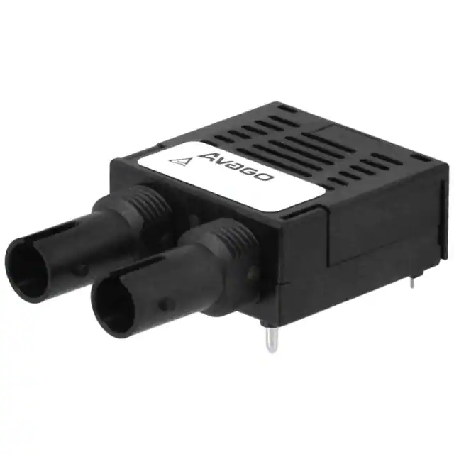
Package
The overall package concept for the Broadcom transceivers
consists of the following basic elements: two optical
subassemblies, an electrical subassembly, and the housing as
illustrated in Figure 1 and Figure 2.
The package outline drawings and pin out are shown in
Figure 3, Figure 4, and Figure 5. The details of this package
outline and pin out are compliant with the multi-source
definition of the 1 × 9 SIP. The low profile of the Broadcom
transceiver design complies with the maximum height allowed
for the duplex SC connector over the entire length of the
package.
The optical subassemblies use a high-volume assembly
process together with low-cost lens elements, which result in a
cost effective building block.
The electrical subassembly consists of a high-volume
multilayer printed circuit board on which the IC chips and
various surface-mounted passive circuit elements are attached.
The package includes internal shields for the electrical and
optical subassemblies to ensure low EMI emissions and high
immunity to external EMI fields.
The outer housing, including the duplex SC connector
receptacle or the duplex ST ports, is molded of filled
nonconductive plastic to provide mechanical strength and
electrical isolation. The solder posts of the Broadcom design
are isolated from the circuit design of the transceiver and do
not require connection to a ground plane on the circuit board.
The transceiver is attached to a printed circuit board with the
nine signal pins and the two solder posts, which exit the
bottom of the housing. The two solder posts provide the
primary mechanical strength to withstand the loads imposed
on the transceiver by mating with duplex or simplex SC or ST
connectored fiber cables.
Figure 1 SC Connector Block Diagram
ELECTRICAL SUBASSEMBLY
DUPLEX SC
RECEPTACLE
DIFFERENTIAL
DATA OUT
PIN PHOTODIODE
SINGLE-ENDED
SIGNAL
DETECT OUT
QUANTIZER IC
PREAMP IC
OPTICAL
SUBASSEMBLIES
DIFFERENTIAL
LED
DATA IN
DRIVER IC
TOP VIEW
Broadcom
-2-
�AFBR-5803AQZ and AFBR-5803ATQZ
Data Sheet
Figure 2 ST Connector Block Diagram
ELECTRICAL SUBASSEMBLY
DUPLEX ST
RECEPTACLE
DIFFERENTIAL
DATA OUT
PIN PHOTODIODE
SINGLE-ENDED
SIGNAL
DETECT OUT
QUANTIZER IC
PREAMP IC
OPTICAL
SUBASSEMBLIES
DIFFERENTIAL
LED
DATA IN
DRIVER IC
TOP VIEW
Broadcom
-3-
�AFBR-5803AQZ and AFBR-5803ATQZ
Data Sheet
Figure 3 SC Connector Package Outline Drawing with Standard Height
AREA FOR LABEL
39.12
MAX.
(1.540)
12.70
(0.500)
6.35
(0.250)
AREA
RESERVED
FOR
PROCESS
PLUG
25.40
MAX.
(1.000)
AVAGO
AFBR-5803AQZ
PHILIPPINES
DATE CODE (YYWW)
12.70
(0.500)
5.93 ± 0.1
(0.233 ± 0.004)
Case Temperature
Measurement Point
+ 0.08
– 0.05
(0.030 + 0.003 )
– 0.002
0.75
3.3 ± 0.4
(0.130 ± 0.016)
3.30 ± 0.38
(0.130 ± 0.015)
10.35 MAX.
(0.407)
2.92
(0.115)
Ø
23.55
(0.927)
0.46
(9x)
(0.018)
NOTE 1
20.32 [8x(2.54/.100)]
(0.800)
4.14
(0.163)
1.27 + 0.25
– 0.05
(0.050 + 0.010 )
– 0.002
NOTE 1
17.32 20.32
(0.682) (0.800)
16.70
(0.657)
0.87
(0.034)
Note 1:
18.52
(0.729)
23.24
(0.915)
15.88
(0.625)
Phosphor bronze is the base material for the posts & pins. For lead-free soldering, the solder posts
have Tin Copper over Nickel plating, and the electrical pins have pure Tin over Nickel plating.
DIMENSIONS ARE IN MILLIMETERS (INCHES).
Broadcom
-4-
23.32
(0.918)
�AFBR-5803AQZ and AFBR-5803ATQZ
Data Sheet
Figure 4 ST Connector Package Outline Drawing with Standard Height
20.32 ± 0.4
[0.80 ± 0.02]
O
6
2. 0]
1
0.
[O
3.6
[0.14]
Dimensions in Millimeters [Inches]
20.9
[0.82]
20.32
[0.800]
2.54 8x
[0.100]
17.4
[0.69]
20.32
[0.800]
21.4
[0.84]
1.3
[0.05]
18.62
[0.733]
23.48
[0.924]
O 0.46
[0.018]
O 1.27
[0.050]
2.6 ± 0.4
[0.10 ± 0.02]
0.5
[0.02]
3.3 ± 0.4
[0.13 ± 0.02]
24.9
[0.98]
e
Ar
25.4
[1.00]
6.0
[0.24]
12.0
[0.47]
12.7
[0.50]
or
af
be
La
l
Case Temperature
Measurement Point
42.0
[1.653]
Broadcom
-5-
�AFBR-5803AQZ and AFBR-5803ATQZ
Data Sheet
Figure 5 Pin Out Diagram
1 = V EE
N/C
2 = RD
Rx
3 = RD
4 = SD
5 = V CC
6 = V CC
7 = TD
Tx
8 = TD
9=V
N/C
EE
TOP VIEW
Application Information
The Applications Engineering group in the Broadcom Fiber
Optics Communication Division is available to assist you with
the technical understanding and design trade-offs associated
with these transceivers. You can contact them through your
Broadcom sales representative.
The following information is provided to answer some of the
most common questions about the use of these parts.
Transceiver Optical Power Budget versus
Link Length
Optical Power Budget (OPB) is the available optical power for a
fiber optic link to accommodate fiber cable losses plus losses
due to inline connectors, splices, optical switches, and to
provide margin for link aging and unplanned losses due to
cable plant reconfiguration or repair.
Figure 6 illustrates the predicted OPB associated with the
transceiver series specified in this data sheet at the Beginning
of Life (BOL). These curves represent the attenuation and
chromatic plus modal dispersion losses associated with the
62.5/125-μm and 50/125-μm fiber cables only. The area under
the curves represents the remaining OPB at any link length,
which is available for overcoming non-fiber cable-related
losses.
Broadcom LED technology has produced 1300-nm LED devices
with lower aging characteristics than normally associated with
these technologies in the industry. The industry convention is
1.5-dB aging for 1300-nm LEDs. The Broadcom 1300-nm LEDs
will experience less than 1 dB of aging over normal commercial
equipment mission life periods. Contact your Broadcom sales
representative for additional details.
Figure 6 was generated with a Broadcom fiber-optic link model
containing the current industry conventions for fiber cable
specifications and the FDDI PMD and LCF-PMD optical
parameters. These parameters are reflected in the guaranteed
performance of the transceiver specifications in this data
sheet.This same model has been used extensively in the ANSI
and IEEE committees, including the ANSI X3T9.5 committee, to
establish the optical performance requirements for various
fiber-optic interface standards. The cable parameters used
come from the ISO/IEC JTC1/SC 25/WG3 Generic Cabling for
Customer Premises per DIS 11801 document and the
EIA/TIA-568-A Commercial Building Telecommunications
Cabling Standard per SP-2840.
Transceiver Signaling Operating Rate
Range and BER Performance
For purposes of definition, the symbol (Baud) rate, also called
signaling rate, is the reciprocal of the shortest symbol time.
Data rate (bits/s) is the symbol rate divided by the encoding
factor used to encode the data (symbols/bit).
When used in Fast Ethernet, FDDI, and ATM 100-Mb/s
applications, the performance of the 1300-nm transceivers is
guaranteed over the signaling rate of 10 MBd to 125 MBd to the
full conditions listed in individual product specification tables.
The transceivers may be used for other applications at
signaling rates outside of the 10-MBd to 125-MBd range with
some penalty in the link optical power budget primarily caused
by a reduction of receiver sensitivity. Figure 7 gives an
indication of the typical performance of these 1300-nm
products at different rates.
These transceivers can also be used for applications that
require different Bit Error Rate (BER) performance. Figure 8
illustrates the typical trade-off between link BER and the
receivers’ input optical power level.
Broadcom
-6-
�AFBR-5803AQZ and AFBR-5803ATQZ
Data Sheet
Figure 6 Optical Power Budget at BOL vs. Fiber-Optic Cable Length
TRANSCEIVER RELATIVE OPTICAL POWER BUDGET AT CONSTANT BER (dB)
12
AFBR-5803, 62.5/125 μm
OPTICAL POWER BUDGET (dB)
10
8
AFBR-5803
50/125 μm
6
4
2
0
0.3 0.5
1.0
1.5
2.0
2.5
FIBER OPTIC CABLE LENGTH (km)
Figure 8 Bit Error Rate vs. Relative Receiver Input Optical Power
1 x 10
1 x 10
Figure 7 Transceiver Relative Optical Power Budget at Constant
BER vs. Signaling Rate
2.5
2.0
CONDITIONS:
1. PRBS 2 7-1
2. DATA SAMPLED AT
CENTER OF DATA SYMBOL.
3. BER = 10 -6
4. T A = +25° C
5. V CC = 3.3 V to 5 V dc
6. INPUT OPTICAL RISE/
FALL TIMES = 1.0/2.1 ns.
1.5
1.0
0.5
0
0.5
25
0
50
75 100 125 150
SIGNAL RATE (MBd)
175 200
Figure 9 Recommended Decoupling and Termination Circuits
-2
-3
Rx
BIT ERROR RATE
1 x 10
1 x 10
Tx
-4
AFBR-5803 SERIES
-5
NO INTERNAL CONNECTION
NO INTERNAL CONNECTION
-6
1 x 10
-7
1 x 10 -8
1 x 10 -9
1 x 10
1 x 10 -10
1 x 10 -11
1 x 10 -12
CENTER OF SYMBOL
AFBR-5803Z
TOP VIEW
-6
-4
-2
0
2
RELATIVE INPUT OPTICAL POWER - dB
Rx
V EE
1
4
CONDITIONS:
1. 155 MBd
2. PRBS 2 7-1
3. CENTER OF SYMBOL SAMPLING
4. T A = +25°C
5. V CC = 3.3 V to 5 V dc
6. INPUT OPTICAL RISE/FALL TIMES = 1.0/2.1 ns.
RD
2
RD
3
Rx
V CC
5
SD
4
Tx
V CC
6
C1
TD
7
Tx
V EE
9
TD
8
C2
V CC
L1
TERMINATION
AT PHY
DEVICE
INPUTS
V CC
R5
R8
RD
SD
V CC
TERMINATION
AT TRANSCEIVER
INPUTS
TD
NOTES:
THE SPLIT-LOAD TERMINATIONS FOR ECL SIGNALS NEED TO BE LOCATED AT THE INPUT
OF DEVICES RECEIVING THOSE ECL SIGNALS. RECOMMEND 4-LAYER PRINTED CIRCUIT
BOARD WITH 50 OHM MICROSTRIP SIGNAL PATHS BE USED.
R1 = R4 = R6 = R8 = R10 = 130 OHMS FOR +5.0 V OPERATION, 82 OHMS FOR +3.3 V OPERATION.
R2 = R3 = R5 = R7 = R9 = 82 OHMS FOR +5.0 V OPERATION, 130 OHMS FOR +3.3 V OPERATION.
C1 = C2 = C3 = C5 = C6 = 0.1 μF.
C4 = 10 μF.
L1 = L2 = 1 μH COIL OR FERRITE INDUCTOR.
Broadcom
-7-
R4
C5
R10
RD
R3
R1
C3
C4
V CC FILTER
AT V CC PINS
TRANSCEIVER
R9
R7
C6
R6
R2
L2
TD
�AFBR-5803AQZ and AFBR-5803ATQZ
Data Sheet
Transceiver Jitter Performance
The Broadcom 1300-nm transceivers are designed to operate
per the system jitter allocations stated in Tables E1 of Annexes
E of the FDDI PMD and LCF-PMD standards.
The Broadcom 1300-nm transmitters will tolerate the
worst-case input electrical jitter allowed in these tables
without violating the worst case output jitter requirements of
Sections 8.1 Active Output Interface of the FDDI PMD and
LCF-PMD standards.
The Broadcom 1300-nm receivers will tolerate the worst-case
input optical jitter allowed in Sections 8.2 Active Input
Interface of the FDDI PMD and LCF-PMD standards without
violating the worst case output electrical jitter allowed in the
Tables E1 of the Annexes E.
The jitter specifications stated in the following 1300-nm
transceiver specification tables are derived from the values in
Tables E1 of Annexes E. They represent the worst-case jitter
contribution that the transceivers are allowed to make to the
overall system jitter without violating the Annex E allocation
example. In practice, the typical contribution of the Broadcom
transceivers is well below these maximum allowed amounts.
Board Layout – Decoupling Circuit and
Ground Planes
It is important to take care in the layout of your circuit board to
achieve optimum performance from these transceivers.
Figure 9 provides a good example of a schematic for a power
supply decoupling circuit that works well with these parts. It is
further recommended that a contiguous ground plane be
provided in the circuit board directly under the transceiver to
provide a low inductance ground for signal return current. This
recommendation is in keeping with good high-frequency
board layout practices.
Board Layout – Hole Pattern
The Broadcom transceiver complies with the circuit board
“Common Transceiver Footprint” hole pattern defined in the
original multisource announcement that defined the 1 × 9
package style. This drawing is reproduced in Figure 10 with the
addition of ANSI Y14.5M compliant dimensioning to be used as
a guide in the mechanical layout of your circuit board.
Board Layout – Mechanical
For applications providing a choice of either a duplex SC or a
duplex ST connector interface, while using the same pinout on
the printed circuit board, the ST port needs to protrude from
the chassis panel a minimum of 9.53 mm for sufficient
clearance to install the ST connector.
Recommended Handling Precautions
Broadcom recommends that normal static precautions be
taken in the handling and assembly of these transceivers to
prevent damage that may be induced by electrostatic
discharge (ESD). The AFBR-5800 series of transceivers meet
MIL-STD-883C Method 3015.4 Class 2 products.
See Figure 11 for a mechanical layout detailing the
recommended location of the duplex SC and duplex ST
transceiver packages in relation to the chassis panel.
Care should be used to avoid shorting the receiver data or
signal detect outputs directly to ground without proper
current limiting impedance.
Solder and Wash Process Compatibility
The transceivers are delivered with protective process plugs
inserted into the duplex SC or duplex ST connector receptacle.
This process plug protects the optical subassemblies during
wave solder and aqueous wash processing and acts as a dust
cover during shipping.
These transceivers are compatible with either industry
standard wave or hand solder processes.
Shipping Container
The transceiver is packaged in a shipping container designed
to protect it from mechanical and ESD damage during
shipment or storage.
Broadcom
-8-
�AFBR-5803AQZ and AFBR-5803ATQZ
Data Sheet
Figure 10 Recommended Board Layout Hole Pattern
20.32
(0.800)
2 x Ø 1.9 ± 0.1
(0.075 ± 0.004)
20.32
(0.800)
2.54
(0.100)
9 x Ø 0.8 ± 0.1
(0.032 ± 0.004)
TOP VIEW
DIMENSIONS ARE IN MILLIMETERS (INCHES)
Broadcom
-9-
�AFBR-5803AQZ and AFBR-5803ATQZ
Data Sheet
Figure 11 Recommended Common Mechanical Layout for SC and ST 1 × 9 Connectored Transceivers
42.0
12.0
24.9
9.53
(NOTE 1)
0.51
12.09
25.4
39.12
11.1
6.79
0.75
25.4
NOTE 1: MINIMUM DISTANCE FROM FRONT
OF CONNECTOR TO THE PANEL FACE.
Regulatory Compliance
Electrostatic Discharge (ESD)
These transceiver products are intended to enable commercial
system designers to develop equipment that complies with the
various international regulations governing certification of
Information Technology Equipment. See Regulatory
Compliance Table for details. Additional information is
available from your Broadcom sales representative.
Immunity to ESD damage is important in two cases.
The first case is during handling of the transceiver prior to
mounting it on the circuit board. It is important to use normal
ESD-handling precautions for ESD-sensitive devices. These
precautions include using grounded wrist straps, work
benches, and floor mats in ESD-controlled areas.
The second case to consider is static discharges to the exterior
of the equipment chassis containing the transceiver parts. To
the extent that the duplex SC connector is exposed to the
outside of the equipment chassis, it may be subject to
whatever ESD system level test criteria that the equipment is
intended to meet.
Broadcom
- 10 -
�AFBR-5803AQZ and AFBR-5803ATQZ
Data Sheet
Regulatory Compliance Table
Feature
Test Method
Performance
Electrostatic Discharge (ESD) to the
Electrical Pins
MIL-STD-883
Method 3015.4
Meets Class 1 (


 工商网监
湘ICP备2023018690号
工商网监
湘ICP备2023018690号
