ASMT-UWB1-Zxxxx
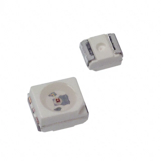
OneWhite Surface Mount PLCC-2 LED Indicator
Description
This family of SMT LEDs is packaged in the industry
standard PLCC-2 package. These SMT LEDs have high
reliability performance and are designed to work under a
wide range of environmental conditions. This high
reliability feature makes them ideally suited to be used as
interior signs application conditions.
These LEDs are compatible with reflow soldering process.
The wide viewing angle at 120° makes these LEDs ideally
suited for panel, push button, offi ce equipment, industrial
equipment, and home appliances. The fl at top emitting
surface makes it easy for these LEDs to mate with light
pipes. With the built-in refl ector pushing up the intensity
of the light output, these LEDs are also suitable to be used
as LED pixels in interior electronic signs.
Features
•
•
•
•
•
•
High reliability package with silicone
encapsulation
Compatible with refl ow soldering process
High optical effi ciency with 100 lm/W
Available in 8 mm carrier tape with reel diameter
180mm
JEDEC MSL 3 product
ESD threshold of 1000 V (HBM model) per Jedec
Applications
• Non-automotive use
• General Signage backlighting
• Amusement machine backlighting
• Industrial lighting
• Light strips
CAUTION: ASMT-UWB1-Zxxxx LEDs are Class 1C ESD sensitive. Please observe appropriate precautions during handling
and processing. Refer to Avago Application Note AN-1142 for additional details.
�Package Dimensions
Notes:
1. All dimensions in millimeters.
2. Terminal finish = Ag plating.
�Device Selection Guide
Color
White
White
White
White
White
White
White
White
White
White
White
White
White
White
White
White
White
White
White
White
White
White
Part Number
ASMT-UWB1-ZX302
ASMT-UWB1-ZX312
ASMT-UWB1-ZX3A2
ASMT-UWB1-ZX3B2
ASMT-UWB1-ZX3C2
ASMT-UWB1-ZX3D2
ASMT-UWB1-ZX3E2
ASMT-UWB1-ZX3F2
ASMT-UWB1-ZX3G2
ASMT-UWB1-ZX3H2
ASMT-UWB1-ZX3J2
ASMT-UWB1-ZAAB2
ASMT-UWB1-ZAAC2
ASMT-UWB1-ZAAD2
ASMT-UWB1-ZAAF2
ASMT-UWB1-ZAAH2
ASMT-UWB1-ZX702
ASMT-UWB1-ZX7A2
ASMT-UWB1-ZX7B2
ASMT-UWB1-ZX7C2
ASMT-UWB1-ZX7D2
ASMT-UWB1-ZX7E2
CCT
(K)
4500 ~ 8000
2700 ~ 4000
8000
6500
5700
5000
4500
4000
3500
3000
2700
6500
5700
5000
4000
3000
4500 ~ 8000
8000
6500
5700
5000
4500
Luminous Intensity (mcd)
Min
Max
1800.00
3550.00
1800.00
3550.00
1800.00
3550.00
1800.00
3550.00
1800.00
3550.00
1800.00
3550.00
1800.00
3550.00
1800.00
3550.00
1800.00
3550.00
1800.00
3550.00
1800.00
3550.00
2000.00
2500.00
2000.00
2500.00
2000.00
2500.00
2000.00
2500.00
2000.00
2500.00
2240.00
4500.00
2240.00
4500.00
2240.00
4500.00
2240.00
4500.00
2240.00
4500.00
2240.00
4500.00
[1,2]
Test Current
(mA)
20
20
20
20
20
20
20
20
20
20
20
20
20
20
20
20
20
20
20
20
20
20
Chip
InGaN
InGaN
InGaN
InGaN
InGaN
InGaN
InGaN
InGaN
InGaN
InGaN
InGaN
InGaN
InGaN
InGaN
InGaN
InGaN
InGaN
InGaN
InGaN
InGaN
InGaN
InGaN
Notes:
1. The luminous intensity IV, is measured at the mechanical axis of the lamp package. The actual peak of the spatial radiation pattern may not be
aligned with this axis.
2. IV Tolerance = ±12%
�Part Numbering System
A S M T
- U x1 B 1
-
Z x2 x3 x4 x5
Packaging Option
Color Bin Selection
Intensity Bin Selection
LED Chip Color
W - White
Table 2. Absolute Maximum Ratings (T A = 25 °C)
Parameters
[1]
DC Forward Current
[2]
Peak Forward Current
Power Dissipation
Junction Temperature
Operating Temperature
Storage Temperature
Rating
30mA
100mA
108 mW
110 °C
- 40 °C to + 85°C
- 40 °C to + 100 °C
Notes:
1. Derate linearly as shown in derating curve.
2. Duty Factor = 10%, Frequency = 1kHz. ommended.
Table 3. Optical Characteristics (T A = 25 °C)
Color
White
Part Number
ASMT-UWB1-Z
Dice
Technology
InGaN
Typ.
Chromaticity
(1)
Coordinates
X
y
0.33 0.34
Viewing Angle
[2]
2θ ½ (Degrees)
Typ.
120
Luminous
Efficiency
η e (lm/W)
Typ.
100
Total Flux /
Luminous Intensity
θ V (lm) / Iv(cd)
Typ.
2.7
Notes:
1. The chromaticity coordinates are derived from the CIE 1931 Chromaticity Diagram and represent the perceived color of the device
2. θ ½ is the off-axis angle where the luminous intensity is ½ the peak intensity.
Table 4. Electrical Characteristics (T A = 25 °C)
Forward Voltage
V F (Volts) @ I F = 20mA
Min.
Max.
2.8
3.6
Reverse Voltage
(1)
V R @ 10μA
Min.
5
Thermal Resistance
Color
Part Number
Rθ J-P (°C/W)
White
ASMT-UWB1-Z
150
Note:
1. Reverse Voltage indicates product fi nal test condition. Long term reverse bias is not recommended.
CRI
Min.
70
�Figure 1. Forward Current Vs. Forward Voltage
Figure 2. Relative Intensity Vs. Forward Current
Figure 3. Chromaticity shift vs. current
Figure 4. Radiation pattern
Figure 5. Maximum forward current vs. ambient temperature.
Derated based on Tjmax 110° C, Rthja 600°C/W
Figure 6. Recommended Pb-free refl ow soldering profi le
�Figure 7. Recommended Pick and Place Nozzle Size
Figure 8. Recommended Soldering Pad Pattern
Figure 9. Tape Leader and Trailer Dimensions
Figure 10. Tape Dimensions (Unit: mm)
Intensity Bin Select (X 2 X 3 )
Color Bin Select (X 4 )
�Individual reel will contain parts from one half bin only
X 2 Min I V Bin
X3
0
3
4
5
B
6
7
8
9
Full Distribution
3 half bins starting from X 2 1
4 half bins starting from X 2 1
2 half bins starting from X 2 1
1 half bins starting from X 2 2
2 half bins starting from X 2 2
3 half bins starting from X 2 2
4 half bins starting from X 2 2
2 half bins starting from X 2 2
Intensity Bin Limits
Bin ID
Min. (mcd)
Max. (mcd)
X1
1800.00
2240.00
X2
2240.00
2850.00
Y1
2850.00
3550.00
Y2
3550.00
4500.00
Z1
4500.00
5600.00
Z2
5600.00
7150.00
AA
2000.00
2500.00
Tolerance of each bin limit = ± 12%
Individual reel will contain parts from one full bin only.
X4
BIn
Color Bin ID
A
1A, 1B, 1C, 1D
B
2A, 2B, 2C, 2D
C
3A, 3B, 3C, 3D
D
4A, 4B, 4C, 4D
E
5A, 5B, 5C, 5D
F
6A, 6B, 6C, 6D
G
7A, 7B, 7C, 7D
H
8A, 8B, 8C, 8D
J
9A, 9B, 9C, 9D
K
1A, 1B, 1C, 1D, 2A, 2B, 2C, 2D,
L
2A, 2B, 2C, 2D, 3A, 3B, 3C, 3D
M
3A, 3B, 3C, 3D, 4A, 4B, 4C, 4D
N
4A, 4B, 4C, 4D, 5A, 5B, 5C, 5D
Q
6A, 6B, 6C, 6D, 7A, 7B, 7C, 7D
R
7A, 7B, 7C, 7D, 8A, 8B, 8C, 8D
S
8A, 8B, 8C, 8D, 9A, 9B, 9C, 9D
0
1A, 1B, 1C, 1D, 2A, 2B, 2C, 2D, 3A, 3B, 3C, 3D,
4A, 4B, 4C, 4D, 5A, 5B, 5C, 5D
1
6A, 6B, 6C, 6D, 7A, 7B, 7C, 7D, 8A, 8B, 8C, 8D,
9A, 9B, 9C, 9D
�Colro Bin ID Limits
Color
Bin ID
1A
1B
1C
1D
2A
2B
2C
2D
3A
3B
3C
3D
4A
Chromaticity Coordinates Limits
x
0.2950 0.2920 0.2984
y
0.2970 0.3060 0.3133
x
0.2920 0.2895 0.2962
y
0.3060 0.3135 0.3220
x
0.2984 0.2962 0.3028
y
0.3133 0.3220 0.3304
x
0.2984 0.3048 0.3068
y
0.3133 0.3207 0.3113
x
0.3048 0.3130 0.3144
y
0.3207 0.3290 0.3186
x
0.3028 0.3115 0.3130
y
0.3304 0.3391 0.3290
x
0.3115 0.3205 0.3213
y
0.3391 0.3481 0.3373
x
0.3130 0.3213 0.3221
y
0.3290 0.3373 0.3261
x
0.3215 0.3290 0.3290
y
0.3350 0.3417 0.3300
x
0.3207 0.3290 0.3290
y
0.3462 0.3538 0.3417
x
0.3290 0.3376 0.3371
y
0.3538 0.3616 0.3490
x
0.3290 0.3371 0.3366
y
0.3417 0.3490 0.3369
x
0.3371 0.3451
y
0.3490 0.3554
4B
x
0.3376 0.3463
y
0.3616 0.3687
4C
x
0.3463 0.3551
y
0.3687 0.3760
4D
x
0.3451 0.3533
y
0.3554 0.3620
5A
x
0.3530 0.3615
y
0.3597 0.3659
5B
x
0.3548 0.3641
y
0.3736 0.3804
5C
x
0.3641 0.3736
y
0.3804 0.3874
5D
x
0.3615 0.3702
y
0.3659 0.3722
Tolerance of each bin limit = ±0.01
0.3440
0.3427
0.3451
0.3554
0.3533
0.3620
0.3515
0.3487
0.3590
0.3521
0.3615
0.3659
0.3702
0.3722
0.3670
0.3578
0.3009
0.3042
0.2984
0.3133
0.3048
0.3207
0.3009
0.3042
0.3068
0.3113
0.3048
0.3207
0.3130
0.3290
0.3144
0.3186
0.3222
0.3243
0.3215
0.3350
0.3290
0.3417
0.3290
0.3300
0.3366
0.3369
0.3371
0.349
0.3451
0.3554
0.3440
0.3427
0.3512
0.3465
0.3530
0.3597
0.3615
0.3659
0.3590
0.3521
Color
Bin ID
6A
6B
6C
6D
7A
7B
7C
7D
8A
8B
8C
8D
9A
Chromaticity Coordinates Limits
x
0.3670 0.3702 0.3825
y
0.3578 0.3722 0.3798
x
0.3702 0.3736 0.3869
y
0.3722 0.3874 0.3958
x
0.3825 0.3869 0.4006
y
0.3798 0.3958 0.4044
x
0.3783 0.3825 0.3950
y
0.3646 0.3798 0.3875
x
0.3889 0.3941 0.4080
y
0.3690 0.3848 0.3916
x
0.3941 0.3996 0.4146
y
0.3848 0.4015 0.4089
x
0.4080 0.4146 0.4299
y
0.3916 0.4089 0.4165
x
0.4017 0.4080 0.4221
y
0.3751 0.3916 0.3984
x
0.4147 0.4221 0.4342
y
0.3814 0.3984 0.4028
x
0.4221 0.4299 0.443
y
0.3984 0.4165 0.4212
x
0.4342 0.4430 0.4562
y
0.4028 0.4212 0.426
x
0.4259 0.4342 0.4465
y
0.3853 0.4028 0.4071
x
0.4373 0.4465
y
0.3893 0.4071
9B
x
0.4465 0.4562
y
0.4071 0.4260
9C
x
0.4582 0.4687
y
0.4099 0.4289
9D
x
0.4483 0.4582
y
0.3919 0.4099
Tolerance of each bin limit = ±0.01
0.4582
0.4099
0.4687
0.4289
0.4813
0.4319
0.4700
0.4126
0.3783
0.3646
0.3825
0.3798
0.3950
0.3875
0.3898
0.3716
0.4017
0.3751
0.4080
0.3916
0.4221
0.3984
0.4147
0.3814
0.4259
0.3853
0.4342
0.4028
0.4465
0.4071
0.4373
0.3893
0.4483
0.3919
0.4582
0.4099
0.4700
0.4126
0.4593
0.3944
�Figure 11. Color Bins
Packaging Option (X5)
Option
2
Test Current
20mA
Package Type
Top Mount
Forward Voltage Bin
Reel Size
7 Inch
Bin ID
Min
F05
2.8
F06
3.0
F07
3.2
F08
3.4
Tolerance of each bin limit = ±0.1 V
Max
3.0
3.2
3.4
3.6
DISCLAIMER: Avago’s products and software are not specifically designed, manufactured or authorized for sale as parts,
components or assemblies for the planning, construction, maintenance or direct operation of a nuclear facility or for use
in medical devices or applications. Customer is solely responsible, and waives all rights to make claims against avago or its
suppliers, for all loss, damage, expense or liability in connection with such use.
For product information and a complete list of distributors, please go to our web site:
www.avagotech.com
Avago, Avago Technologies, and the A logo are trademarks of Avago Technologies in the United States
and other countries.
Data subject to change. Copyright © 2005-2011 Avago Technologies. All rights reserved.
April 23, 2013
�