DMB53D0UDW
N-CHANNEL ENHANCEMENT MODE MOSFET PLUS NPN TRANSISTOR
Features
Mechanical Data
N-Channel MOSFET and NPN Transistor in One Package
Low On-Resistance
Very Low Gate Threshold Voltage, 1.0V max
Low Input Capacitance
Fast Switching Speed
Low Input/Output Leakage
Ultra-Small Surface Mount Package
ESD Protected MOSFET Gate up to 2kV
Totally Lead-Free & Fully RoHS Compliant (Notes 1 & 2)
Halogen and Antimony Free. “Green” Device (Note 3)
For automotive applications requiring specific change
control (i.e.: parts qualified to AEC-Q101, PPAP capable, and
manufactured in IATF 16949 certified facilities), please refer
to the related automotive grade (Q-suffix) part. A listing can
be found at
https://www.diodes.com/products/automotive/automotiveproducts/.
This part is qualified to JEDEC standards (as references in
AEC-Q101) for High Reliability.
https://www.diodes.com/quality/product-definitions/
Case: SOT-363
Case Material: Molded Plastic, “Green” Molding Compound.
UL Flammability Classification Rating 94V-0
Moisture Sensitivity: Level 1 per J-STD-020
Terminal Connections: See Diagram
Terminals: Finish - Matte Tin annealed over Alloy 42 Lead frame.
Solderable per MIL-STD-202, Method 208
Marking Information: See Page 5
Ordering Information: See Page 5
Weight: 0.006 grams (approximate)
SOT-363
D2
E
B
Q1
Q2
S2
ESD protected gate up to 2kV
G2
C
TOP VIEW
TOP VIEW
Internal Schematic
Maximum Ratings – MOSFET, Q1 (@TA = +25°C, unless otherwise specified.)
Characteristic
Symbol
VDSS
VGSS
Drain-Source Voltage
Gate-Source Voltage
Drain Current (Note 4)
Continuous
Pulsed Drain Current (Note 4)
Unit
V
V
ID
Value
50
12
160
IDM
560
mA
mA
Maximum Ratings - NPN Transistor, Q2 (@TA = +25°C, unless otherwise specified.)
Characteristic
Collector-Base Voltage
Collector-Emitter Voltage
Emitter-Base Voltage
Collector Current
Symbol
VCBO
VCEO
VEBO
IC
Value
50
45
6.0
100
Unit
V
V
V
mA
Value
250
500
-55 to +150
Unit
mW
C/W
C
Thermal Characteristics, Total Device (@TA = +25°C, unless otherwise specified.)
Characteristic
Total Power Dissipation (Note 4)
Thermal Resistance, Junction to Ambient (Note 4)
Operating and Storage Temperature Range
Notes:
Symbol
PD
RJA
TJ, TSTG
1. No purposely added lead. Fully EU Directive 2002/95/EC (RoHS), 2011/65/EU (RoHS 2) & 2015/863/EU (RoHS 3) compliant.
2. See https://www.diodes.com/quality/lead-free/ for more information about Diodes Incorporated’s definitions of Halogen- and Antimony-free, "Green" and
Lead-free.
3. Halogen- and Antimony-free "Green” products are defined as those which contain
很抱歉,暂时无法提供与“DMB53D0UDW-7”相匹配的价格&库存,您可以联系我们找货
免费人工找货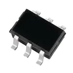


 工商网监
湘ICP备2023018690号
工商网监
湘ICP备2023018690号
