DMB53D0UV
N-CHANNEL ENHANCEMENT MODE MOSFET PLUS NPN TRANSISTOR
Features
Mechanical Data
N-Channel MOSFET and NPN Transistor in One Package
Low On-Resistance
Very Low Gate Threshold Voltage, 1.0V max
Low Input Capacitance
Fast Switching Speed
Low Input/Output Leakage
Ultra-Small Surface Mount Package
ESD Protected MOSFET Gate up to 2kV
Lead, Halogen and Antimony Free, RoHS Compliant (Note 1)
"Green" Device (Note 2)
For automotive applications requiring specific change
control (i.e.: parts qualified to AEC-Q101, PPAP capable, and
manufactured in IATF 16949 certified facilities), please refer
to the related automotive grade (Q-suffix) part. A listing can
be found at
https://www.diodes.com/products/automotive/automotiveproducts/.
This part is qualified to JEDEC standards (as references in
AEC-Q101) for High Reliability.
https://www.diodes.com/quality/product-definitions/
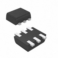
Case: SOT563
Case Material: Molded Plastic, “Green” Molding Compound.
UL Flammability Classification Rating 94V-0
Moisture Sensitivity: Level 1 per J-STD-020
Terminal Connections: See Diagram
Terminals: Finish - Matte Tin annealed over Copper lead frame.
Solderable per MIL-STD-202, Method 208
Weight: 0.006 grams (approximate)
D2
SOT563
B
E
Q1
Q2
S2
C
Top View
Internal Schematic
Bottom View
Top View
ESD PROTECTED TO 2kV
G2
Ordering Information (Note 3)
Part Number
DMB53D0UV-7
DMB53D0UV-13
Notes:
Case
SOT563
SOT563
Packaging
3000/Tape & Reel
10000/Tape & Reel
1. EU Directive 2002/95/EC (RoHS) & 2011/65/EU (RoHS 2) compliant. No purposely added lead. Halogen and Antimony free.
2. Diodes Inc.’s “Green” policy can be found on our website at http://www.diodes.com.
3. For packaging details, go to our website at http://www.diodes.com.
Marking Information
MB1 YM
Date Code Key
Year
Code
2008
V
Month
Code
Jan
1
2009
W
Feb
2
DMB53D0UV
Document number: DS31651 Rev. 8 - 2
2010
X
Mar
3
2011
Y
Apr
4
May
5
MB1 = Marking Code
YM = Date Code Marking
Y = Year (ex: V = 2008)
M = Month (ex: 9 = September)
2012
Z
Jun
6
1 of 7
www.diodes.com
2013
A
Jul
7
2014
B
Aug
8
2015
C
Sep
9
2016
D
Oct
O
2017
E
Nov
N
Dec
D
October 2019
© Diodes Incorporated
�DMB53D0UV
Maximum Ratings – MOSFET, Q1 (@TA = +25°C, unless otherwise specified.)
Characteristic
Drain-Source Voltage
Gate-Source Voltage
Drain Current (Note 4)
Pulsed Drain Current (Note 4)
Symbol
VDSS
VGSS
ID
IDM
Continuous
Value
50
12
160
560
Units
V
V
mA
mA
Maximum Ratings - NPN Transistor, Q2 (@TA = +25°C, unless otherwise specified.)
Characteristic
Symbol
VCBO
VCEO
VEBO
IC
Collector-Base Voltage
Collector-Emitter Voltage
Emitter-Base Voltage
Collector Current
Value
50
45
6.0
100
Unit
V
V
V
mA
Value
250
500
-55 to +150
Unit
mW
C/W
C
Thermal Characteristics, Total Device (@TA = +25°C, unless otherwise specified.)
Characteristic
Total Power Dissipation (Note 1)
Thermal Resistance, Junction to Ambient (Note 1)
Operating and Storage Temperature Range
Symbol
PD
RJA
TJ, TSTG
Electrical Characteristics - MOSFET (@TA = +25°C, unless otherwise specified.)
Characteristic
OFF CHARACTERISTICS (Note 5)
Drain-Source Breakdown Voltage
Zero Gate Voltage Drain Current
Symbol
Min
Typ
Max
Unit
BVDSS
IDSS
50
10
V
A
IGSS
1.0
A
ON CHARACTERISTICS (Note 5)
Gate Threshold Voltage
VGS(th)
Static Drain-Source On-Resistance
RDS (ON)
0.7
0.8
3.1
4
1.0
4
5
Gate-Body Leakage
5.0
V
Forward Transconductance
gFS
180
ms
DYNAMIC CHARACTERISTICS (Note 6)
Input Capacitance
Output Capacitance
Reverse Transfer Capacitance
Ciss
Coss
Crss
25
5
2.1
pF
pF
pF
Notes:
Test Condition
VGS = 0V, ID = 250A
VDS = 50V, VGS = 0V
VGS = 8V, VDS = 0V
VGS = 12V, VDS = 0V
VDS = VGS, ID = 250A
VGS = 4V, ID = 100mA
VGS = 2.5V, ID = 80mA
VDS = 10V, ID = 100mA,
f = 1.0KHz
VDS = 10V, VGS = 0V,
f = 1.0MHz
4. Device mounted on FR-4 substrate PC board, 2oz copper, with minimum recommended pad layout.
5. Short duration pulse test used to minimize self-heating effect.
6. Guaranteed by design. Not subject to product testing.
DMB53D0UV
Document number: DS31651 Rev. 8 - 2
2 of 7
www.diodes.com
October 2019
© Diodes Incorporated
�DMB53D0UV
Electrical Characteristics - NPN Transistor (@TA = +25°C, unless otherwise specified.)
Characteristic
Collector-Base Breakdown Voltage
Collector-Emitter Breakdown Voltage
Emitter-Base Breakdown Voltage
DC Current Gain
(Note 5)
(Note 5)
(Note 5)
(Note 5)
Symbol
V(BR)CBO
V(BR)CEO
V(BR)EBO
hFE
Min
50
45
6
200
Typ
—
—
—
290
Collector-Emitter Saturation Voltage
(Note 5)
VCE(SAT)
—
—
Base-Emitter Saturation Voltage
(Note 5)
VBE(SAT)
—
Base-Emitter Voltage
(Note 5)
VBE
580
—
700
900
660
—
Collector-Cutoff Current
(Note 5)
—
—
Collector-Emitter Cut-Off Current
(Note 5)
ICBO
ICBO
ICES
—
—
700
770
15
5.0
100
fT
100
—
—
MHz
COBO
—
—
4.5
pF
NF
—
—
10
dB
Gain Bandwidth Product
Output Capacitance
Noise Figure
Max
—
—
—
450
100
300
Unit
V
V
V
—
—
mV
mV
mV
nA
µA
nA
Test Condition
IC = 10A, IB = 0
IC = 10mA, IB = 0
IE = 1A, IC = 0
VCE = 5.0V, IC = 2.0mA
IC = 10mA, IB = 0.5mA
IC = 100mA, IB = 5.0mA
IC = 10mA, IB = 0.5mA
IC = 100mA, IB = 5.0mA
VCE = 5.0V, IC = 2.0mA
VCE = 5.0V, IC = 10mA
VCB = 30V
VCB = 30V, TA = +150°C
VCE = 45V
VCE = 5.0V, IC = 10mA,
f = 100MHz
VCB = 10V, f = 1.0MHz
VCE = 5V, RS = 2.0k
f = 1.0kHz, BW= 200Hz
MOSFET
0.8
0.5
VGS = 10V
0.7
VDS = 10V
ID, DRAIN CURRENT (A)
ID, DRAIN CURRENT (A)
0.4
VGS = 4.5V
0.6
0.5
VGS = 3.0V
0.4
VGS = 2.5V
0.3
0.2
= 85癈
TA =TA85°
C
25癈
TTAA==25°
C
T
TAA = -55癈
-55°C
0.3
TTAA==150癈
150°C
TTAA==125癈
125°C
0.2
0.1
0.1
VGS = 1.5V
VGS = 1.0V
0
0
0.5
1
1.5 2 2.5 3 3.5 4 4.5
VDS, DRAIN-SOURCE VOLTAGE (V)
Fig. 1 Typical Output Characteristics
0
0
5
10
VGS = 2.5V
VGS = 4.0V
0.01
0.1
ID, DRAIN CURRENT (A)
Fig. 3 Typical On-Resistance
vs. Drain Current and Gate Voltage
DMB53D0UV
Document number: DS31651 Rev. 8 - 2
1
RDS(ON), DRAIN-SOURCE ON-RESISTANCE ()
RDS(ON), DRAIN-SOURCE ON-RESISTANCE ()
4
Fig. 2 Typical Transfer Characteristics
10
1
0.001
1
2
3
VGS, GATE SOURCE VOLTAGE (V)
3 of 7
www.diodes.com
TAT=A150°
C
= 150癈
T
125癈C
TAA == 125°
85°C
TTAA = 85癈
TTAA =
= 25癈
25°C
TAA== -55°
-55癈
T
C
1
0
0.1
0.2
0.3
0.4
0.5
ID, DRAIN CURRENT (A)
Fig. 4 Typical Drain-Source On-Resistance
vs. Drain Current and Temperature
October 2019
© Diodes Incorporated
�DMB53D0UV
2.0
35
30
VGS = 4V
ID = 100mA
1.6
1.4
C, CAPACITANCE (pF)
RDS(ON), DRAIN-TO-SOURCE
RESISTANCE (NORMALIZED)
1.8
VGS = 2.5V
ID = 80mA
1.2
1.0
0.8
25
20
f = 1MHz
VGS = 0V
15
10
5
0.6
0.4
-50
0
1.1
1
-25
0
25
50
75 100 125 150
(°C))
TJ, JUNCTION TEMPERATURE (癈
Fig. 5 On-Resistance Variation with Temperature
VGS(TH), GATE THRESHOLD VOLTAGE (V)
Ciss
Coss
Crss
0
5
10
15
20
25
30
35
VDS, DRAIN-SOURCE VOLTAGE (V)
Fig. 6 Typical Capacitance
40
0.9
IS, SOURCE CURRENT (A)
1.0
ID = 250礎
ID=250A
0.8
0.7
0.1
TA T
=A150°
C
= 150癈
125癈
TTAA==125°
C
0.01
85癈
TTAA==85°
C
0.001
25°C
TTAA== 25癈
TT
A ==-55癈
-55°C
A
0.6
0.5
-50
-25
0
25
50
75 100 125 150
(°C))
TA, AMBIENT TEMPERATURE (癈
Fig. 7 Gate Threshold Variation vs. Ambient Temperature
0.0001
0.1
0.3
0.5
0.7
0.9
1.1
VSD, SOURCE-DRAIN VOLTAGE (V)
Fig. 8 Diode Forward Voltage vs. Current
PD, POWER DISSIPATION (mW)
300
250
200
150
100
50
RJA = 500C/W
0
-50
0
50
100
150
TA, AMBIENT TEMPERATURE (°C)
Fig. 9 Derating Curve - Total Package Power Dissipation
DMB53D0UV
Document number: DS31651 Rev. 8 - 2
4 of 7
www.diodes.com
October 2019
© Diodes Incorporated
�DMB53D0UV
NPN Transistor
1,000
0.4
TA = 150°C
IC
IB = 20
100
VCE(SAT), COLLECTOR-EMITTER
SATURATION VOLTAGE (V)
hFE, DC CURRENT GAIN
TA = 25°C
TA = -50°C
10
1
100
1,000
10
IC, COLLECTOR CURRENT (mA)
Fig. 10 Typical DC Current Gain vs. Collector Current
1
0.3
0.2
25癈
TTAA==25°
C
TAT= =150°
C
150癈
A
0.1
-50°C
TTAA== -50癈
0
0.1
1,000
1
10
100
IC, COLLECTOR CURRENT (mA)
Fig. 11 Typical Collector-Emitter Saturation Voltage
vs. Collector Current
fT, GAIN-BANDWIDTH PRODUCT (MHz)
1,000
VCE = 5V
100
10
1
1
10
IC, COLLECTOR CURRENT (mA)
Fig. 12 Typical Gain-Bandwidth Product
vs. Collector Current
DMB53D0UV
Document number: DS31651 Rev. 8 - 2
100
5 of 7
www.diodes.com
October 2019
© Diodes Incorporated
�DMB53D0UV
Package Outline Dimensions
Please see http://www.diodes.com/package-outlines.html for the latest version.
A
B
SOT563
Dim Min
Max Typ
A
0.15 0.30 0.20
B
1.10 1.25 1.20
C
1.55 1.70 1.60
D
0.50
G
0.90 1.10 1.00
H
1.50 1.70 1.60
K
0.55 0.60 0.60
L
0.10 0.30 0.20
M
0.10 0.18 0.11
All Dimensions in mm
C
D
G
M
K
H
L
Suggested Pad Layout
Please see http://www.diodes.com/package-outlines.html for the latest version.
C2
Z
C2
C1
G
Y
Dimensions Value (in mm)
Z
2.2
G
1.2
X
0.375
Y
0.5
C1
1.7
C2
0.5
X
DMB53D0UV
Document number: DS31651 Rev. 8 - 2
6 of 7
www.diodes.com
October 2019
© Diodes Incorporated
�DMB53D0UV
IMPORTANT NOTICE
DIODES INCORPORATED MAKES NO WARRANTY OF ANY KIND, EXPRESS OR IMPLIED, WITH REGARDS TO THIS DOCUMENT,
INCLUDING, BUT NOT LIMITED TO, THE IMPLIED WARRANTIES OF MERCHANTABILITY AND FITNESS FOR A PARTICULAR PURPOSE
(AND THEIR EQUIVALENTS UNDER THE LAWS OF ANY JURISDICTION).
Diodes Incorporated and its subsidiaries reserve the right to make modifications, enhancements, improvements, corrections or other changes
without further notice to this document and any product described herein. Diodes Incorporated does not assume any liability arising out of the
application or use of this document or any product described herein; neither does Diodes Incorporated convey any license under its patent or
trademark rights, nor the rights of others. Any Customer or user of this document or products described herein in such applications shall assume
all risks of such use and will agree to hold Diodes Incorporated and all the companies whose products are represented on Diodes Incorporated
website, harmless against all damages.
Diodes Incorporated does not warrant or accept any liability whatsoever in respect of any products purchased through unauthorized sales channel.
Should Customers purchase or use Diodes Incorporated products for any unintended or unauthorized application, Customers shall indemnify and
hold Diodes Incorporated and its representatives harmless against all claims, damages, expenses, and attorney fees arising out of, directly or
indirectly, any claim of personal injury or death associated with such unintended or unauthorized application.
Products described herein may be covered by one or more United States, international or foreign patents pending. Product names and markings
noted herein may also be covered by one or more United States, international or foreign trademarks.
This document is written in English but may be translated into multiple languages for reference. Only the English version of this document is the
final and determinative format released by Diodes Incorporated.
LIFE SUPPORT
Diodes Incorporated products are specifically not authorized for use as critical components in life support devices or systems without the express
written approval of the Chief Executive Officer of Diodes Incorporated. As used herein:
A. Life support devices or systems are devices or systems which:
1. are intended to implant into the body, or
2. support or sustain life and whose failure to perform when properly used in accordance with instructions for use provided in the
labeling can be reasonably expected to result in significant injury to the user.
B. A critical component is any component in a life support device or system whose failure to perform can be reasonably expected to cause the
failure of the life support device or to affect its safety or effectiveness.
Customers represent that they have all necessary expertise in the safety and regulatory ramifications of their life support devices or systems, and
acknowledge and agree that they are solely responsible for all legal, regulatory and safety-related requirements concerning their products and any
use of Diodes Incorporated products in such safety-critical, life support devices or systems, notwithstanding any devices- or systems-related
information or support that may be provided by Diodes Incorporated. Further, Customers must fully indemnify Diodes Incorporated and its
representatives against any damages arising out of the use of Diodes Incorporated products in such safety-critical, life support devices or systems.
Copyright © 2019, Diodes Incorporated
www.diodes.com
DMB53D0UV
Document number: DS31651 Rev. 8 - 2
7 of 7
www.diodes.com
October 2019
© Diodes Incorporated
�


 工商网监
湘ICP备2023018690号
工商网监
湘ICP备2023018690号

