A product Line of
Diodes Incorporated
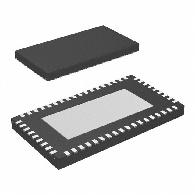
PI3EQX12908A2
8-channel PCI Express Gen 3, 10GbE, SATA3 ReDriver™ with Linear Equalization
Features
Description
ÎÎHigh-speed serial link with linear equalizer
The PI3EQX12908A2 is an 8-channel PCIe Gen 2, 10GbE, SATA3,
ReDriver™. The device provides programmable linear equalization, output swing and gain, by either pin strapping option or
I2C Control, to optimize performance over a variety of physical
mediums by reducing Inter-symbol interference.
ÎÎSupport PCIe Gen 1/2/3 protocol, 10GbE, SATA3, SAS3
ÎÎSupporting 8 differential channels
ÎÎIndependent channel configuration of receiver equalization,
output swing and flat gain
The PI3EQX12908A2 supports eight 100-Ohm Differential CML
data I/O’s and extends the signals across other distant data pathways on the user’s platform.
ÎÎPer Channel Activity Detector with selectable input
termination between 50Ω to VDD and 200KΩ to VDD
Per Channel Output Termination Detector on power up with
ÎÎ
The programmable settings can be applied easily via pins, software (I2C) or loaded via an external EEPROM. When operating
in the EEPROM mode, the configuration information is automatically loaded on power up, which eliminates the need for an
external microprocessor or software driver.
selectable output termination between 50Ω to VDD and High
impedance
ÎÎVery linear transfer function
ÎÎFully compliant to PCISIG Link Training
ÎÎSingle-ended mode receiver detection for PCIe
The PI3EQX12908A2 offers fully Linear Transfer function to fully comply with all PCIe 3 Link Training signals.
ÎÎInput Threshold detection
ÎÎPin strap and I2C master/slave selectable device
programming with external EEPROM
ÎÎ4-bit selectable address bit for I2C
ÎÎSupply Voltage: 3.3V±0.3V
ÎÎIndustrial Temperature Range: -40oC to 85oC
ÎÎPackaging (Pb-free & Green):
àà 54-contact TQFN (10mm x 5.5mm x 0.5mm pitch) flowthrough pinout
Eye Diagram
Before Channel Loss
Before ReDriver
After ReDriver
Pericom
ReDriver
Host
Channel Loss
TX +
RX +
-
PI3EQX12908A2
Document Number DS40411 Rev 1-2
Long input trace,
cable, or connectors
Long output trace,
cable, or connectors
Device
Equalizer, De-emphasis,
Swing, and Amplifier Gain
End Point
+
+
-
-
+
+
-
-
1
Output trace
Input trace
+ RX
+ TX
-
www.diodes.com
November 2017
Diodes Incorporated
�A product Line of
Diodes Incorporated
PI3EQX12908A2
Block Diagram
Input Threshold
Detection
Conditional
Output Load:
100-Ohm diff.
or Hi-Z
Rx detect
CML Input
Buffer
-
I+
Linear
Amplifier
Equalizer
+
II+
Buff r
er
Conditional
Input Load:
VDD 50-Ohm or
200K-ohm
ut
Equalization
Control (4-bit)
Flat gain
control
Flat gain
control (2-bits)
Power
Management
PRSNT#
Buffer
O+
I++
+
-
Swing
Control
Voltage
mode
output
buffer
I+
O-
Output Swing
control (1-bit)
Repeats for 8 Channel
EQB1/AD2
EQB0/AD3
VDD
FGA1/SCL
FGA0/SDA
ENI2C
FGB0/AD1
PRSNT#
FGB1/AD0
Pin Configuration - Top View (54-TQFN)
54 53 52 51 50 49 48 47 46
B0RX+
1
45
B0TX+
B0RXB1RX+
B1RX-
2
3
44
B0TXB1TX+
43
42
41
4
5
6
7
B2RX+
B2RXB3RX+
B3RX-
40
8
9
VDD
10
A0RX+
A0RX-
GND
B1TXVDD
39
B2TX+
B2TX-
38
37
B3TX+
B3TX-
36
35
34
VDD
A0TX+
A0TX-
A1RX+
11
12
A1RXVDD
A2RX+
13
14
15
33
32
31
A1TX+
A1TXA2TX+
A2RX-
16
17
30
A3RX+
A2TXA3TX+
A3RX-
18
29
28
A3TX-
PI3EQX12908A2
Document Number DS40411 Rev 1-2
SD_TH0
ALL_DONE
GND
SW0/I2C_RESET#
RXDET
EQB2
EQA0
EQA1
EQA2
19 20 21 22 23 24 25 26 27
2
www.diodes.com
November 2017
Diodes Incorporated
�A product Line of
Diodes Incorporated
PI3EQX12908A2
Pin Description
(Flow-Thru Pinout)
Pin # (54-TQFN)
Pin Name
Type Description
Data Signals
10
A0RX+
I
11
A0RX-
I
35
A0TX+,
O
34
A0TX-
O
12
A1RX+,
I
13
A1RX-
I
33
A1TX+,
O
32
A1TX-
O
15
A2RX+,
I
16
A2RX-
I
31
A2TX+,
O
30
A2TX-
O
17
A3RX+,
I
18
A3RX-
I
29
A3TX+,
O
28
A3TX-
O
1
B0RX+,
I
2
B0RX-
I
45
B0TX+,
O
44
B0TX-
O
3
B1RX+,
I
4
B1RX-
I
43
B1TX+,
O
42
B1TX-
O
5
B2RX+,
I
6
B2RX-
I
40
B2TX+,
O
39
B2TX-
O
7
B3RX+,
I
8
B3RX-
I
38
B3TX+,
O
37
B3TX-
O
PI3EQX12908A2
Document Number DS40411 Rev 1-2
Differential inputs for Channel A0, with internal 50-Ohm pull-up and >200K-Ohm
otherwise.
Differential outputs for Channel A0
Differential inputs for Channel A1, with internal 50-Ohm pull-up and >200K-Ohm
otherwise.
Differential outputs for Channel A1
Differential inputs for Channel A2, with internal 50-Ohm pull-up and >200K-Ohm
otherwise.
Differential outputs for Channel A2
Differential inputs for Channel A3, with internal 50-Ohm pull-up and >200K-Ohm
otherwise.
Differential outputs for Channel A3
Differential inputs for Channel B0, with internal 50-Ohm pullup and >200KOhm
otherwise.
Differential outputs for Channel B0
Differential inputs for Channel B1, with internal 50-Ohm pullup and >200KOhm
otherwise.
Differential outputs for Channel B1
Differential inputs for Channel B2, with internal 50-Ohm pullup and >200KOhm
otherwise.
Differential outputs for Channel B2
Differential inputs for Channel B3, with internal 50-Ohm pullup and >200KOhm
otherwise.
Differential outputs for Channel B3
3
www.diodes.com
November 2017
Diodes Incorporated
�A product Line of
Diodes Incorporated
PI3EQX12908A2
Pin Description Cont.
Pin # (54-TQFN)
Pin Name
Type Description
Control Signals
48
ENI2C
I
I2C Enable Pin. When tied to Low, each channel is programmed by the external
pin voltage (Pin Mode). When tied to High, each channel is programmed by the
data stored in the I2C bus (Slave Mode). When FLOAT, data is accesses from
external EEPROM (Master Mode). ENI2C has pull-up / pull-down 90k-Ohm
resistance (Default = VDD / 2).
When ENI2C = 1 (I2C Mode)
50
SCL
I/O
I2C SCL clock input in I2C Slave Mode (ENI2C = High). This pin becomes clock
output when loading from EEPROM in I2C Master Mode (ENI2C = FLOAT).
49
SDA
I/O
I2C SDA data input/output in I2C Master or Slave Mode.
I2C programmable address bits in I2C Master or Slave Mode. AD[0:2] have pullup 90k-Ohm resistance. AD[3] have pull-up / pull-down 90k-Ohm resistance.
(Default = VDD/2)
54, 53, 47, 46
AD[0:3]
I
25
I2C_RESET#
I
Reset Pin for I2C. When Low, the registers are reset to default value.
I2C_RESET# has pull-up 90k-Ohm resistance
I
These pins set the level of Equalizer in Bank A channels when ENI2C is Low.
When ENI2C is High, the I2C registers provide independent control of each
channel. See Table 1: Equalizer Settings. EQA[1] has pull-up 90k-Ohm resistance.
EQA[0] and EQA[2] have pull-up / pull-down 90k-Ohm resistance (Default =
VDD / 2).
I
These pins set the level of Equalizer in Bank B channels when ENI2C is Low.
When ENI2C is High, the I2C registers provide independent control of each
channel, and the EQB[1:0] pins are converted to I2C AD[2:3] inputs. See Table 1:
Equalizer Settings. EQB[1] has pull-up 90k-Ohm resistance. EQB[0] and EQB[2]
have pull-up / pull-down 90k-Ohm resistance (Default = VDD / 2).
I
These pins control the level of Flat Gain in Bank A channels when ENI2C is Low.
When ENI2C is High, the I2C registers provide independent control of each
channel, and the FGA[1:0] pins are converted to I2C SCL/SDA. See Table 2: Flat
Gain Settings.
When ENI2C = 0 (Pin mode)
21, 20, 19
46, 47, 23
49, 50
EQA[0:2]
EQB[0:2]
FGA[0:1]
53, 54
FGB[0:1]
I
These pins control the level of Flat Gain in Bank B channels when ENI2C is Low.
When ENI2C is High, the I2C registers provide independent control of each
channel, and FGB[1:0] pins are converted to AD[0:1] inputs. See Table 2: Flat Gain
Settings. FGB[0] and FGB[1] have pull-up 90k-Ohm resistance.
25
SW0
I
This pins sets the Output Voltage Swing level in all channels when ENI2C is Low.
SW0 has pull-up 90k-Ohm resistance.
26
SD_TH0
I
Internal Signal Detect Threshold. This pin should be tied to VDD for normal
operation. Refer to Table 4 for more options. SD_TH0 has pull-up 90k-Ohm
resistance.
I
Receiver Detection Control Pin. When High, receiver detection is enabled to
support PCIe Mode. When Low, receiver detection is disabled to support 10GbE
and SATA3 Modes and input is 50-Ohm to VDD. RXDET has pull-up 90k-Ohm
resistance.
In both I2C and Pin modes
22
PI3EQX12908A2
Document Number DS40411 Rev 1-2
RXDET
4
www.diodes.com
November 2017
Diodes Incorporated
�A product Line of
Diodes Incorporated
PI3EQX12908A2
Pin Description Cont.
Pin # (54-TQFN)
52
Pin Name
Type Description
PRSNT#
I
Cable Present Detect Input. When High, a cable is not present per PCIe Cabling
Specification 1.0, and the device is put in lower power mode. When Low, the
device is enabled and in normal operation. PRSNT# has pull-up 90k-Ohm resistance.
ALL_DONE
O
Valid Register Load Status Output. When LOW, the external EEPROM load has
failed. When HIGH, the external EEPROM load is successful.
Output
27
Power Pins
9, 14, 36, 41, 51
VDD
PWR
3.3V ± 10% Supply Voltage
Center Pad, 24
GND
PWR
Supply GND
PI3EQX12908A2
Document Number DS40411 Rev 1-2
5
www.diodes.com
November 2017
Diodes Incorporated
�A product Line of
Diodes Incorporated
PI3EQX12908A2
Description of Operation
Output Receiver Detector:
On power up or when PRSNT# becomes low, the output resistance is set to high impedance, and the input resistance is set to 200K
ohms. The device continually looks to detect an external 50 ohm termination resistor on a per channel basis. If no 50 ohms is detected
in the first 40us of time, the channel is continually polled with 40us detection cycle until detection occurs. This operation can only be
reinitiated when PRSNT# or I2C_RESET# are toggled again.
Input Activity Detector:
When the input voltage on individual channel basis falls below Vth-, the output is driven to the common mode voltage so as to eliminate
output chatter. When the input voltage is higher than Vth+, the channel is resumed immediately.
Power Enable function:
One pin control or I2C control, when PRSNT# is set to high, the IC goes into power down mode, both input and output termination set
to 200K and high impedance respectively. Individual channel enabling is done through the I2C register programming.
Equalization Setting:
EQA[2:0] and EQB[2:0] are the selection pins for the equalization selection for each of the channels of A and B respectively.
Table 1. Equalization Setting
Equalizer setting (dB)
EQ2
EQ1
EQ0
EQ 4 Bits
@ 1.25GHz
@ 2.5GHz
@ 3GHz
@ 4GHz
@ 5GHz
@ 6GHz
0
0
0
0000
0
0.6
1.0
1.5
2.4
2.8
0
0
1
0001
0.15
1.2
1.7
2.4
3.5
4
0
1
0
0010
0.4
1.9
2.5
3.3
4.5
5
0
1
1
0011
0.6
2.5
3.2
4.2
5.3
5.8
1
0
0
0100
1.8
3.4
4.1
4.9
6.0
6.4
1
0
1
0101
2.1
3.9
4.7
5.6
6.7
7.1
1
1
0
0110
2.3
4.4
5.2
6.2
7.3
7.7
1
1
1
0111
2.5
4.9
5.7
6.8
7.9
8.2
HIZ
0
0
1000
3.4
5.6
6.4
7.3
8.4
8.7
HIZ
0
1
1001
3.6
6.0
6.9
7.8
8.9
9.1
HIZ
1
0
1010
3.8
6.4
7.3
8.3
9.3
9.5
HIZ
1
1
1011
4.1
6.8
7.7
8.7
9.7
9.9
0
0
HIZ
1100
5.1
7.5
8.3
9.2
10.1
10.2
0
1
HIZ
1101
5.3
7.8
8.6
9.5
10.4
10.5
1
0
HIZ
1110
5.4
8.1
8.9
9.8
10.7
10.8
1
1
HIZ
1111
5.6
8.4
9.2
10.1
11
11.1
PI3EQX12908A2
Document Number DS40411 Rev 1-2
6
www.diodes.com
November 2017
Diodes Incorporated
�A product Line of
Diodes Incorporated
PI3EQX12908A2
Flat Gain Setting:
Output Swing Setting:
Table 2. Flat Gain Setting
Table 3. Output Swing Setting
SW0 is the selection bit for output swing for A and B channels.
Flat Gain settings: FGA[0:1] and FGB[0:1] are the selection bits
for Flat Gain value for A and B channels.
FGA1
FGB1
FGA0
FGB0
(dB)
0
0
-4
0
1
-2
1
0
0
1
1
2
SW0
mVp-p
0
900
1
1,000
Signal Detect Threshold Level:
Table 4. Signal Detect Threshold Level Setting via I2C Bus Mode
SD_TH1
PI3EQX12908A2
SD_TH0
Threshold ON (mVppd)
Threshold OFF (mVppd)
0
0
130
30
0
1
150
50
1
0
170
70
1
1
210
110
Document Number DS40411 Rev 1-2
7
www.diodes.com
November 2017
Diodes Incorporated
�A product Line of
Diodes Incorporated
PI3EQX12908A2
I2C Programming
Address assignment
A6
A5
A4
A3
A2
A1
A0
R/W
1
1
1
AD3
AD2
AD1
AD0
1=R, 0=W
BYTE 0
Bit
Type
Power up condition
Control affected
7
R
A3 Signal Detector Output
6
R
A2 Signal Detector Output
5
R
A1 Signal Detector Output
4
R
A0 Signal Detector Output
3
R
B3 Signal Detector Output
2
R
B2 Signal Detector Output
1
R
B1 Signal Detector Output
0
R
B0 Signal Detector Output
Comment
1= Activity 0=no
activity
BYTE 1
Bit
Type
Power up condition
Control affected
7
R
A3 RX Detector Output
6
R
A2 RX Detector Output
5
R
A1 RX Detector Output
4
R
A0 RX Detector Output
3
R
B3 RX Detector Output
2
R
B2 RX Detector Output
1
R
B1 RX Detector Output
0
R
B0 RX Detector Output
Comment
1 = Far-end 50
-ohm detected
0 = Not detected
BYTE 2
Bit
Type
Power up condition
Control affected
7
R/W
0
A3 Power down
6
R/W
0
A2 Power down
5
R/W
0
A1 Power down
4
R/W
0
A0 Power down
3
R/W
0
B3 Power down
2
R/W
0
B2 Power down
1
R/W
0
B1 Power down
0
R/W
0
PI3EQX12908A2
Document Number DS40411 Rev 1-2
Comment
1 = Power down
B0 Power down
8
www.diodes.com
November 2017
Diodes Incorporated
�A product Line of
Diodes Incorporated
PI3EQX12908A2
I2C Programming Cont.
BYTE 3
Bit
Type
Power up condition
Control affected
7
R/W
0
EQ3
6
R/W
0
EQ2
Equalizer
5
R/W
0
EQ1
See Table 1
4
R/W
0
3
R/W
0
2
R/W
0
FG0
Flat Gain
See Table 2
1
R/W
0
Reserved
Swing
0
R/W
0
SW0
See Table 3
Bit
Type
Power up condition
Control affected
Comment
7
R/W
0
EQ3
6
R/W
0
EQ2
Equalizer
5
R/W
0
EQ1
See Table 1
4
R/W
0
3
R/W
0
2
R/W
0
FG0
Flat Gain
See Table 2
1
R/W
0
Reserved
Swing
0
R/W
0
SW0
See Table 3
Bit
Type
Power up condition
Control affected
Comment
7
R/W
0
EQ3
6
R/W
0
5
R/W
0
4
R/W
0
EQ0
3
R/W
0
FG1
2
R/W
0
FG0
Flat Gain
See Table 2
1
R/W
0
Reserved
Swing
0
R/W
0
SW0
See Table 3
Comment
EQ0
Channel A0 configuration
FG1
BYTE 4
EQ0
Channel A1 configuration
FG1
BYTE 5
PI3EQX12908A2
Document Number DS40411 Rev 1-2
Channel A2 configuration
9
EQ2
Equalizer
EQ1
See Table 1
www.diodes.com
November 2017
Diodes Incorporated
�A product Line of
Diodes Incorporated
PI3EQX12908A2
I2C Programming Cont.
BYTE 6
Bit
Type
Power up condition
Control affected
7
R/W
0
EQ3
6
R/W
0
EQ2
Equalizer
5
R/W
0
EQ1
See Table 1
4
R/W
0
3
R/W
0
2
R/W
0
FG0
Flat Gain
See Table 2
1
R/W
0
Reserved
Swing
0
R/W
0
SW0
See Table 3
Bit
Type
Power up condition
Control affected
Comment
7
R/W
0
EQ3
6
R/W
0
EQ2
Equalizer
5
R/W
0
EQ1
See Table 1
4
R/W
0
3
R/W
0
2
R/W
0
FG0
Flat Gain
See Table 2
1
R/W
0
Reserved
Swing
0
R/W
0
SW0
See Table 3
Bit
Type
Power up condition
Control affected
Comment
7
R/W
0
EQ3
6
R/W
0
EQ2
Equalizer
5
R/W
0
EQ1
See Table 1
4
R/W
0
3
R/W
0
2
R/W
0
FG0
Flat Gain
See Table 2
1
R/W
0
Reserved
Swing
0
R/W
0
SW0
See Table 3
Channel A3 configuration
Comment
EQ0
FG1
BYTE 7
Channel B0 configuration
EQ0
FG1
BYTE 8
PI3EQX12908A2
Document Number DS40411 Rev 1-2
Channel B1 configuration
EQ0
FG1
10
www.diodes.com
November 2017
Diodes Incorporated
�A product Line of
Diodes Incorporated
PI3EQX12908A2
I2C Programming Cont.
BYTE 9
Bit
Type
Power up condition
Control affected
7
R/W
0
EQ3
6
R/W
0
EQ2
Equalizer
5
R/W
0
EQ1
See Table 1
4
R/W
0
3
R/W
0
2
R/W
0
FG0
Flat Gain
See Table 2
1
R/W
0
Reserved
Swing
0
R/W
0
SW0
See Table 3
Bit
Type
Power up condition
Control affected
Comment
7
R/W
0
EQ3
6
R/W
0
EQ2
Equalizer
5
R/W
0
EQ1
See Table 1
4
R/W
0
3
R/W
0
2
R/W
0
FG0
Flat Gain
See Table 2
1
R/W
0
Reserved
Swing
0
R/W
0
SW0
See Table 3
Bit
Type
Power up condition
Control affected
Comment
7
R/W
0
A3 Signal Detector
6
R/W
0
A2 Signal Detector
5
R/W
0
A1 Signal Detector
4
R/W
0
A0 Signal Detector
3
R/W
0
B3 Signal Detector
2
R/W
0
B2 Signal Detector
1
R/W
0
B1 Signal Detector
0
R/W
0
B0 Signal Detector
Channel B2 configuration
Comment
EQ0
FG1
BYTE 10
Channel B3 configuration
EQ0
FG1
BYTE 11
1=Power Down
PI3EQX12908A2
Document Number DS40411 Rev 1-2
11
www.diodes.com
November 2017
Diodes Incorporated
�A product Line of
Diodes Incorporated
PI3EQX12908A2
I2C Programming Cont.
BYTE 12
Bit
Type
Power up condition
Control affected
7
R/W
0
A3 RX Detector
6
R/W
0
A2 RX Detector
5
R/W
0
A1 RX Detector
4
R/W
0
A0 RX Detector
3
R/W
0
B3 RX Detector
2
R/W
0
B2 RX Detector
1
R/W
0
B1 RX Detector
0
R/W
0
B0 RX Detector
Bit
Type
Power up condition
Control affected
7
R/W
0
6
R/W
0
5
R/W
0
4
R/W
0
3
R/W
0
2
R/W
0
1
R/W
0
SD_TH1
0
R/W
0
SD_TH0
Comment
1=Power Down
1=disable
BYTE 13
Comment
Reserved
Signal Detector
Threshold
BYTE 14 to 15 have '0' as Power-up condition
PI3EQX12908A2
Document Number DS40411 Rev 1-2
12
www.diodes.com
November 2017
Diodes Incorporated
�A product Line of
Diodes Incorporated
PI3EQX12908A2
Reset and I2C Master Timing Diagram
I2C_RESET#
Trstpw
Trstd
SCL/SDA
ENI2C
Master
Load
I2C_RESET#
HIZ condition
Recommended minimum reset pulse width Trstpw= 1μs
I2C master cycle start from I2C_RESET# pulse go high, Trstd = 200μs
ENI2C = HIZ to I2C_RESET#(high) (min), Ti2cm_rst = 1 uS.
I2C Operation
The integrated I2C interface operates as a master or slave device depending on the pin ENI2C being HIZ or HIGH respectively. Standard mode (100Kbps) is supported with 7-bit addressing. The data byte format is 8-bit bytes, and supports the format of indexing to be
compatible with other bus devices. In the Slave mode (ENI2C = HIGH), the device supports Read/Write. The bytes must be accessed in
sequential order from the lowest to the highest byte with the ability to stop after any complete byte has been transferred.
Address bits A3 to A0 are programmable to support multiple chips environment. The Data is loaded until a Stop sequence is issued.
In the master mode (ENI2C = HIZ), PI3EQX12908A2 supports up to 16 masters connected in daisy chain through connecting I2C_
DONE pin to I2C_RESET# pin of the next part.
Master EEPROM data starting address of the device address is indicated in the table below:
AD3, AD2,AD1,AD0
EEPROM Data Starting Location
0000
00h
0001
10h
0010
20h
0011
30h
0100
40h
0101
50h
0110
60h
0111
70h
1000
80h
1001
90h
1010
A0h
1011
B0h
1100
C0h
1101
D0h
1110
E0h
1111
F0h
PI3EQX12908A2
Document Number DS40411 Rev 1-2
13
www.diodes.com
November 2017
Diodes Incorporated
�A product Line of
Diodes Incorporated
PI3EQX12908A2
When tying multiple PI3EQX12908A2 devices to the SDA and SCL bus, use the guidelines below to configure the devices. The user also
can refer the application notes for detail information.
• Use AD[3:0] address bits so that each device can loaded it's configuration from the EEPROM.
Example below is for 4 devices. The first device in the sequence must be address 0x00h;
subsequent devices must follow the address order listed below.
– U1: AD[3:0] = 0000 = 0x00h,
– U2: AD[3:0] = 0001 = 0x10h,
– U3: AD[3:0] = 0010 = 0x20h,
– U4: AD[3:0] = 0011 = 0x30h
• For I2C Slave Mode operation, use a 2Kohms pull-up resistor on SDA and SCL pins. For I2C Master Mode operation, use a 1Kohm
pull-up resistor on SDA and SCL pins.
• Daisy-chain I2C_RESET# and ALL_DONE from one device to the next device in the sequence so that they do not compete for the
EEPROM at the same time.
1. Tie ALL_DONE of U1 to I2C_RESET# of U2
2. Tie ALL_DONE of U2 to I2C_RESET# of U3
3. Tie ALL_DONE of U3 to I2C_RESET# of U4
4. Optional: Tie ALL_DONE output of U4 to a LED to show the devices has been loaded successfully
Below is an example of a 2 kbits (256 x 8-bit) EEPROM in hex format for 4pcs PI3EQX12908A2 device. Bold fonts in yellow are register
setting from Byte0 to Byte15 for each device in each line. Bold fonts in red is the EEPROM data location.
:10000000000000FF0000FFFFFFFFFF0000FF620194
:10001000000000FFFF0000FFFFFFFF0000FF620184
:10002000000000FFFFFF0000FFFFFF0000FF620174
:10003000000000FFFFFFFF0000FFFF0000FF620164
:1000400000000000000000000000000000000000B0
:1000500000000000000000000000000000000000A0
:100060000000000000000000000000000000000090
:100070000000000000000000000000000000000080
:100080000000000000000000000000000000000070
:100090000000000000000000000000000000000060
:1000A0000000000000000000000000000000000050
:1000B0000000000000000000000000000000000040
:1000C0000000000000000000000000000000000030
:1000D0000000000000000000000000000000000020
:1000E0000000000000000000000000000000000010
:1000F0000000000000000000000000000000000000
:00000001FF
2k bits (256 x 8-bit) EEPROM Date Example
Below is the sample of the I2C master reading waveform based on the setup above.
PI3EQX12908A2
Document Number DS40411 Rev 1-2
14
www.diodes.com
November 2017
Diodes Incorporated
�A product Line of
Diodes Incorporated
PI3EQX12908A2
SCL Synchronization
When more than one I2C device becomes a master device and drives the SCL line, each device senses the state of SCL line and automatically adjust the the drive timing by adjusting the timing to the timing to the slowest one.
SCL
Macro A
SCLO
(Before arbitration)
SCLO
(After arbitration)
After SCL line has become “H”, take the
timing until the next state of SCLO = L
After SCL line has become “H”, take the
timing until the next state of SCLO = L
Macro B
SCLO
(Before arbitration)
SCLO
(After arbitration)
Transferring Data
Every byte put on the SDA line must be 8-bits long. Each byte has to be followed by an acknowledge bit. Data is transferred with the
most significant bit (MSB) first (see the I2C Data Transfer diagram). The PI3EQX12908A2 will never hold the clock line SCL LOW to
force the master into a wait state.
Acknowledge
Data transfer with acknowledge is required from the master. When the master releases the SDA line (HIGH) during the acknowledge
clock pulse, the PI3EQX12908A2 will pull down the SDA line during the acknowledge clock pulse so that it remains stable LOW during
the HIGH period of this clock pulse as indicated in the I2C Data Transfer diagram. The PI3EQX12908A2 will generate an acknowledge
after each byte has been received.
Data Transfer
A data transfer cycle begins with the master issuing a start bit. After recognizing a start bit, the PI3EQX12908A2 will watch the next
byte of information for a match with its address setting. When a match is found it will respond with a read or write of data on the following clocks. Each byte must be followed by an acknowledge bit, except for the last byte of a read cycle which ends with a stop bit.
For a write cycle, the first data byte following the address byte is an index byte that is used by the PI3EQX12908A2. Data is transferred
with the most significant bit (MSB) first.
PI3EQX12908A2
Document Number DS40411 Rev 1-2
15
www.diodes.com
November 2017
Diodes Incorporated
�A product Line of
Diodes Incorporated
PI3EQX12908A2
I2C Data Transfer
Start & Stop Conditions
A HIGH to LOW transition on the SDA line while SCL is HIGH indicates a START condition. A LOW to HIGH transition on the SDA
line while SCL is HIGH defines a STOP condition, as shown in the figure below. When a STOP condition is detected, index byte value
will be reset to 0.
SDA
SDA
SCL
SCL
S
P
START condition
STOP condition
I2C START and STOP conditions.
I2C Data Transfer Sequence
1.�Read�sequence
ACK
DATA�OUT
ACK
ACK
ACK
ACK
DATA�OUT�N
NO�ACK
DEV�SEL
R�/�W
stop
start
I2C Slave
2.�Write�sequence
ACK
ACK
ACK
DEV�SEL
R�/�W
DATA�IN�N
DATA�IN�1
INDEX BYTE
stop
start
I2C Slave
3.�Combined�sequence
ACK INDEX�BYTE
ACK
ACK DATA�OUT�1 ACK
ACK DATA�OUT�N NO�ACK
PI3EQX12908A2
Document Number DS40411 Rev 1-2
DEV�SEL R�/�W
16
stop
DEV�SEL R�/�W
start
start
I2C Slave
www.diodes.com
Notes:
1. only block read and block write from the lowest byte
November 2017
Diodes Incorporated
�A product Line of
Diodes Incorporated
PI3EQX12908A2
Maximum Ratings
(Above which useful life may be impaired. For user guidelines, not tested.)
Supply Voltage . . . . . . . . . . . . . . . . . . . . . . . . . . . . . . . . . -0.5V to +4.0V
LVCMOS Input/Output Voltage . . . . . . . . . . . . . . . . . . -0.5V to +4.0V
CML Input Voltage . . . . . . . . . . . . . . . . . . . . . . . . . -0.5V to (VDD+0.5)
CML Input Current . . . . . . . . . . . . . . . . . . . . . . . . . . . . -30 to +30 mA
I2C pins . . . . . . . . . . . . . . . . . . . . . . . . . . . . . . . . . . . . . . . . . VDD+0.3 V
Storage Temperature . . . . . . . . . . . . . . . . . . . . . . . . . –65°C to +150°C
Max. Junction Temperature . . . . . . . . . . . . . . . . . . . . . . . . . . . . 125 °C
ESD HBM . . . . . . . . . . . . . . . . . . . . . . . . . . . . . . . . . . . . . . . . . . . . . . 2kV
Note:
Stresses greater than those listed under MAXIMUM
RATINGS may cause permanent damage to the device. This is a stress rating only and functional operation of the device at these or any other conditions
above those indicated in the operational sections of
this specification is not implied. Exposure to absolute
maximum rating conditions for extended periods may
affect reliability.
LVCMOS I/O DC Specifications (VDD = 3.3 ± 10%, TA = -40 to 85°C)
Symbol
Parameter
Conditions
VIH
DC input logic high
VIL
DC input logic low
VOH
DC output logic high
At IOH = -200µA
VOL
DC output logic low
At IOL = +200µA
Vhys
Hysteresis of Schmitt trigger input
Min.
Typ.
Max.
Units
VDD/2 +
0.7
VDD + 0.3
V
-0.3
VDD/2 - 0.7
V
VDD - 0.2
V
0.2
V
0.8
V
SDA and SCL I/O for I2C-bus (VDD = 3.3 ± 10%, TA = -40 to 85°C)
Symbol
Parameter
VIH
DC input logic high
VIL
DC input logic low
VOL
DC output logic low
Vhys
Hysteresis of Schmitt trigger input
tof
Output fall time from VIHmin to
VILmax
f SCLK
SCLK clock frequency
Conditions
Min.
Typ.
Max.
Units
VDD/2 +
0.7
VDD + 0.3
V
-0.3
VDD/2 - 0.7
V
0.4
V
IOL = 3mA
0.8
Bus capacity = 10 to
400pF
V
250
ns
100
kHz
High Speed I/O AC/DC Specifications (VDD = 3.3 ± 10%, TA = -40 to 85°C)
Receiver Input (100Ω differential)
Symbol
Parameter
CRX
RX AC coupling capacitance
S11
PI3EQX12908A2
Document Number DS40411 Rev 1-2
Input return loss
Conditions
Min.
Typ.
Max.
220
10MHz to 4GHz differential
13
1GHz to 4GHz common
mode
4
17
Units
nF
dB
www.diodes.com
November 2017
Diodes Incorporated
�A product Line of
Diodes Incorporated
PI3EQX12908A2
High Speed I/O AC/DC Specifications Cont.
Symbol
S22
Parameter
Output return loss
Conditions
Min.
Typ.
10MHz to 4GHz differential
21
1GHz to 4GHz common
mode
4
Max.
Units
dB
DC single-ended input impedance
50
DC differential input impedance
100
DC single-ended output impedance
50
DC differential output impedance
100
ZRX-HIZ
DC input CM input impedance during reset
or power down
200
VRX-DIFF-PP
Differential Input Peak-to-peak Voltage
Operational
1.2
Vppd
Input source common-mode noise
DC – 200MHz
150
mVppd
4
8
ns
4
8
ns
R IN
ROUT
TTX-IDLE-SET-TOIDLE
Max time to electrical idle after sending an
EIOS
TTX-IDLE-TO-DIFF- Max time to valid diff signal after leaving
Ω
Ω
kΩ
DATA
electrical idle
Vth +
On threshold of signal detector
Signal swing @ 4GHz
130
210
mVppd
Vth -
Off threshold of signal detector
Signal swing @ 100MHz
30
110
mVppd
VDD
Power supply voltage
3.6
V
Pmax
Max Supply power
1
W
Imax
Max Supply current
330
mA
Pidle
Supply power
36
mW
GP5GHZ
Peaking gain (Compensation at 5GHz, relative to 100MHz, 100mVp-p sine wave input)
SW=01, FG=10
GP6GHZ
GF
Peaking gain (Compensation at 6GHz, relative to 100MHz, 100mVp-p sine wave input)
SW=01, FG=10
Flat gain (100MHz, EQ = 1000,
SW = 01)
3
3.3
PRSNT#=0
PRSNT#=1
16.1
13.5
EQ = 1111
EQ = 1000
EQ = 0000
Variation around typical
-3
14.8
-3
+3
+2.0
-0.5
-4.0
-3
+3
-1dB compression point of output swing (at
100MHz)
SW0=1
SW0=0
1000
900
V1dB_6G
-1dB compression point of output swing (at
6GHz) FG= 0dB, EQ = 0000 or 0(h)
SW0=1
600
SW0=0
540
Document Number DS40411 Rev 1-2
18
dB
-2.0
V1dB_100M
PI3EQX12908A2
dB
9.0
FG = 11
FG = 10
FG = 01
FG = 00
Variation around typical
+3
17.2
EQ = 1111
EQ = 1000
EQ = 0000
Variation around typical
dB
8.0
www.diodes.com
mVppd
mVppd
November 2017
Diodes Incorporated
�A product Line of
Diodes Incorporated
PI3EQX12908A2
High Speed I/O AC/DC Specifications Cont.
Symbol
Parameter
Conditions
VCoup
Channel isolation
100MHz to 5GHz, Figure 1 (Note 1)
28
100MHz to 5GHz,
FG = 11, EQ
= 0000, Figure 2
0.5
100MHz to 5GHz,
FG = 11, EQ
= 1010, Figure 2
0.4
100MHz to 5GHz,
FG = 11, EQ
= 0000, Figure 2
0.7
100MHz to 5GHz,
FG = 11, EQ
= 1010, Figure 2
0.8
From input to output
0.2
ns
0.0258
UI
Vnoise_input
Vnoise_output
Input-referred noise
Output-referred noise (Note 2)
Min.
Typ.
Max.
Units
dB
mVRMS
mVRMS
1.6
Latency
tpd
Latency
Jitter
PRBS31@24hrs
Rj
Additive Random Jitter at 8Gb/s (worst
case)
36” 5mils FR4
VID = 0.8mVp-p
DE = 0dB
EQ = 0100
Note 1: Measured using a vector-network analyzer (VNA) with -15dBm power level applied to the adjacent input. The VNA detects the signal at the output of the
victim channel. All other inputs and outputs are terminated with 50Ω.
Note 2: Guaranteed by design and characterization.
PI3EQX12908A2
Document Number DS40411 Rev 1-2
19
www.diodes.com
November 2017
Diodes Incorporated
�A product Line of
Diodes Incorporated
PI3EQX12908A2
Characteristics of the SDA and SCl bus lines for Standard Mode I2C-bus devices(1)
Symbol
Parameter
Conditions
Min.
Typ.
Max.
Units
f SCL
SCL clock frequency
100
_
kHz
tHD;STA
Hold time (repeated) START condition. After this period,
the first clock pulse is generated.
4.0
_
tLOW
LOW period of the SCL clock
4.7
_
tHIGH
HIGH period of the SCL clock
4.0
_
tSU;STA
Set-up time for a repeated START condition
4.7
_
tHD;DAT
Data hold time
10
_
tSU;DAT
Data set-up time
250
_
tr
Rise time of both SDA and SCL signals
-
1000
tf
Fall time of both SDA and SCL signals
tSU;STO
Set-up time for STOP condition
4.0
_
tBUF
Bus free time between a STOP and STOP condition
4.7
_
Cb
Capacitive load for each bus line
-
400
ms
ns
ns
300
ms
pF
Notes:
1. All values referred to VIH min and VIL max levels
PI3EQX12908A2
Document Number DS40411 Rev 1-2
20
www.diodes.com
November 2017
Diodes Incorporated
�A product Line of
Diodes Incorporated
PI3EQX12908A2
4-PORT VECTOR
NETWORK ANALYZER
N52454
AGGRESSOR
SIGNAL
(0dBm)
50Ω
PI3EQX12908A2
50Ω
RX1+
PI3EQX12908A2
RX_+
TX_+
RX_-
TX_-
50Ω
50Ω
RX1-
TX1-
RX2+
TX2+
POWER METER
GIGATRONICS 8652A
WITH 80301A HEAD
(10MHz to 18GHz)
BALUN
PSPL 5315A
(200kHz TO 17GHz)
TX1+
50Ω
VICTIM
INPUT
VICTIM
ONTPUT
50Ω
RX2-
TX2-
Noise Test Configuration
Channel-Isolation Test Configuration
FR4
Signal
Source
A
B
C
D.U.T.
SmA
Connector
SmA
Connector
In
Out
≤30IN
AC Test Circuit Referenced in the Electrical Characteristic Table
PI3EQX12908A2
Document Number DS40411 Rev 1-2
21
www.diodes.com
November 2017
Diodes Incorporated
�A product Line of
Diodes Incorporated
PI3EQX12908A2
STOP
START
START
SDA
tf
tf
tSU;DAT
tLOW
tr
t HD;STA
tBUF
SCL
tHD;STA
S
tHD;DAT
HIGH
t SU;STA
Sr
t SU;STO
P
S
I2C Timing
VD+
Common Mode
Voltage
VCM
VDIFF
VD-
VDIFFp-p
V_D+ - V_D-
0V
VDIFFp-p
Definition of Differential Voltage
and Differential Voltage Peak-to-Peak
PI3EQX12908A2
Document Number DS40411 Rev 1-2
22
www.diodes.com
November 2017
Diodes Incorporated
�A product Line of
Diodes Incorporated
PI3EQX12908A2
Application Diagrams
VDD
50 ohm
220nF
0-48in
50 ohm
220nF
AXRX+
AXTX+
AXRX-
AXTX-
220nF
0-48in
220nF
PI3EQX12908A2
AGND
PRSNT#
VDD
3.3V
SCL
SCL
GND
0V
SDA
SDA
Applications Information
GENERAL RECOMMENDATIONS
The PI3EQX12908A2 is a high performance circuit capable of delivering excellent performance. Careful attention must be paid to the
details associated with high-speed design as well as providing a clean power supply. Refer to the information below and Revision 4 of
the LVDS Owner's Manual for more detailed information on high speed design tips to address signal integrity design issues.
PCB LAYOUT CONSIDERATIONS FOR DIFFERENTIAL PAIRS
The Differential inputs and LPDS outputs have been optimized to work with interconnects using a controlled differential impedance
of 85 - 100Ω. It is preferable to route differential lines exclusively on one layer of the board, particularly for the input traces. The use of
vias should be avoided if possible. If vias must be used, they should be used sparingly and must be placed symmetrically for each side
of a given differential pair. Whenever differential vias are used the layout must also provide for a low inductance path for the return
currents as well. Route the differential signals away from other signals and noise sources on the printed circuit board.
POWER SUPPLY BYPASSING
Two approaches are recommended to ensure that the PI3EQX12908A2 is provided with an adequate power supply. First, the supply
(VDD) and ground (GND) pins should be connected to power planes routed on adjacent layers of theprinted circuit board. The layer
thickness of the dielectric should be minimized so that the VDD and GND planes create a low inductance supply with distributed
capacitance. Second, careful attention to supply bypassing through the proper use of bypass capacitors is required. A 0.1 μF bypass
capacitor should be connected to each VDD pin such that the capacitor is placed as close as possible to the PI3EQX12908A2. Smaller
body size capacitors can help facilitate proper component placement. Additionally, capacitor with capacitance in the range of 1 μF to
10 μF should be incorporated in the power supply bypassing design as well. These capacitors can be either tantalum or an ultra-low
ESR ceramic.
Notes:
Hot Plug Detect feature operation is dependent on certain channel conditions, such as length.
For hot plug detect, reset will automatically go back to receiver detect (RXDET) cycle.
PI3EQX12908A2
Document Number DS40411 Rev 1-2
23
www.diodes.com
November 2017
Diodes Incorporated
�A product Line of
Diodes Incorporated
PI3EQX12908A2
Application Schematics
VDD_3.3V
RX
C1
C2
C3
C4
C5
C6
C7
C8
VDD_3.3V
HOST
TX
H0TX_P
H0TX_N
H1TX_P
H1TX_N
H2TX_P
H2TX_N
H3TX_P
H3TX_N
B0TX+
B0TXB1TX+
B1TXB2TX+
B2TXB3TX+
B3TX-
9
14
VDD
VDD
10
11
12
13
15
16
17
18
A0RX+
A0RXA1RX+
A1RXA2RX+
A2RXA3RX+
A3RX-
24
19
20
21
22
23
24
25
26
27
ps. PI3EQX8908A/10908A pin
is GND(2016Mar22 )
45
44
43
42
40
39
38
37
B0RX+
B0RXB1RX+
B1RXB2RX+
B2RXB3RX+
B3RXVDD
VDD
41
36
A0TX+
A0TXA1TX+
A1TXA2TX+
A2TXA3TX+
A3TX-
35
34
33
32
31
30
29
28
RX
Cn
C9
C10
C11
C12
C13
C14
C15
C16
0.1u_0402
R5
0 ohm or NC
0 ohm or NC
VDD_3.3V
D0RX_P
D0RX_N
D1RX_P
D1RX_N
D2RX_P
D2RX_N
D2RX_P
D2RX_N
0.176uF~0.265uF_0402
0.176uF~0.265uF_0402
0.176uF~0.265uF_0402
0.176uF~0.265uF_0402
0.176uF~0.265uF_0402
0.176uF~0.265uF_0402
0.176uF~0.265uF_0402
0.176uF~0.265uF_0402
TX
VDD_3.3V
R6
SCL/FGA1
VDD_3.3V
0 ohm or NC
R7
0 ohm or NC
S D A/ F G A 0
R8
R9
0 ohm or NC
0 ohm or NC
D1
ALL_DONE#
2 R10
LED_R
ALL_DONE#
R11
0 ohm or NC
0 ohm or NC
FGB1/AD0
R4
Device o r
Connector
0 ohm or NC R14
C18
0.1u_0402
0 ohm or NC R13
C17
I2C_RST/SW0
SD_TH
EQA2
EQA1
EQA0
RX_DET
EQB2
EC1
R3
VDD_3.3V
PI3EQX12908A2ZFE@TQFN54
0 ohm or NC R12
+
1.0uF_0805
0 ohm or NC
FGB0/AD1
D0TX_P
D0TX_N
D1TX_P
D1TX_N
D2TX_P
D2TX_N
D3TX_P
D3TX_N
1
2
3
4
5
6
7
8
1
VDD_3.3V
VDD_3.3V
54
53
52
51
50
49
48
47
46
FGB1/AD0
FGB0/AD1
PRSNT#
0.176uF~0.265uF_0402
0.176uF~0.265uF_0402
0.176uF~0.265uF_0402
0.176uF~0.265uF_0402
0.176uF~0.265uF_0402
0.176uF~0.265uF_0402
0.176uF~0.265uF_0402
0.176uF~0.265uF_0402
FGB1/AD0
FGB0/AD1
PRSNT#
VDD
FGA1/SCL
FGA0/SDA
ENI2C
EQB1/AD2
EQB0/AD3
H0RX_P
H0RX_N
H1RX_P
H1RX_N
H2RX_P
H2RX_N
H3RX_P
H3RX_N
U1
VDD_3.3V
R2
EQA2
EQA1
EQA0
RXDET
EQB2
GND
I2C_Reset#/SW0
SD_TH
ALL_DONE#
Cn
R1
SCL/FGA1
SDA/FGA0
ENI2C
AD2/EQB1
AD3/EQB0
0 ohm or NC
2K ohm
reserve for debug purpose
Attention the IC part
and differential TX AC coupling capacitor value.
PRSNT#
R31
0 ohm
VDD_3.3V
VDD_3.3V
R15
VDD_3.3V
ENI2C
R40
I2C_RST//SW 0
0 ohm or NC
VDD_3.3V
R16
0 ohm or NC
VDD_3.3V
R17
VDD_3.3V
R18
VDD_3.3V
R19
R20
0 ohm or NC
0 ohm or NC
0 ohm or NC
0 ohm or NC
AD3/EQB0
SD_TH
EQB2
EQA2
0 ohm or NC
R23
R24
R25
R26
R27
R28
0 ohm or NC
0 ohm or NC
0 ohm or NC
0 ohm or NC
0 ohm or NC
0 ohm or NC
EQA0
Speed
Location
8Gbps
IC Part
PI3EQX12908A2
Cn
0.176uF~0.265uF
10Gbps
PI3EQX12908A2
10GBASE-KR: 0.1uF
10GBASE-KX4: 4.7nF
R33
0 ohm or NC
SCL/DEMA1/FGA1 0 ohm or NC
SDA/DEMA0/FGA0 0 ohm or NC
ENI2C=NC(Master
R11=NC, R19 =NC
mode)
ENI2C=High (I2C co
R11=on, R19 =NC
SDA/DEMA0/FGA0
R3 2 =0 o h m
SDA/ DEMA0 / FGA0
R32=0ohm
SCL/DEMA1/FGA1
R31=0ohm
SCL/DEMA1/FGA1
R31=0ohm
I2C SDA /
EEPROMSDA
I2C SCL /
EEPROMSCL
Connect to EEPROM SDA
Connect to EEPROM SCL
PI3EQX12908A2
Document Number DS40411 Rev 1-2
I2C SDA /
EEPROMSDA
I2C SCL /
EEPROMSCL
ntrol)
Connect to I2C SDA
Connect to I2C SCL
ENI2C=Low (Pin strap c
R11=NC , R19 =on
SDA/DEMA0/FGA0
SCL/DEMA1/FGA1
I2C SDA /
EEPROMSDA
I2C SCL /
EEPROMSCL
R31
R32
I2C SDA / EEPROM SDA
I2C SCL / EEPROM SCL
ontrol)
R32=NC
R31=NC
NC
NC
24
www.diodes.com
November 2017
Diodes Incorporated
�A product Line of
Diodes Incorporated
PI3EQX12908A2
Packaging Information 54-TQFN (ZF)
16-0180
Thermal Resistance - 54-contact ZF Package/72-contact ZL Package:
θJC......................................................................................................11.5°C/W
θJA......................................................No Airflow, 4 layer JEDEC 19.1°C/W
For latest package info.
please check: http://www.diodes.com/design/support/packaging/pericom-packaging/packaging-mechanicals-and-thermal-characteristics/
Ordering Information
Ordering Number
PI3EQX12908A2ZFEX
Package Code
ZF
Package Description
54-Contact, Very Thin Quad Flat No-Lead (TQFN)
Notes:
• Thermal characteristics can be found on the company web site at www.diodes.com/design/support/packaging/
• E = Pb-free and Green
• X suffix = Tape/Reel
PI3EQX12908A2
Document Number DS40411 Rev 1-2
25
www.diodes.com
November 2017
Diodes Incorporated
�A product Line of
Diodes Incorporated
PI3EQX12908A2
IMPORTANT NOTICE
DIODES INCORPORATED MAKES NO WARRANTY OF ANY KIND, EXPRESS OR IMPLIED, WITH REGARDS TO THIS DOCUMENT, INCLUDING, BUT NOT
LIMITED TO, THE IMPLIED WARRANTIES OF MERCHANTABILITY AND FITNESS FOR A PARTICULAR PURPOSE (AND THEIR EQUIVALENTS UNDER
THE LAWS OF ANY JURISDICTION).
Diodes Incorporated and its subsidiaries reserve the right to make modifications, enhancements, improvements, corrections or other changes without further notice to this document and any product described herein. Diodes Incorporated does not assume any liability arising out of the application or use of this document or
any product described herein; neither does Diodes Incorporated convey any license under its patent or trademark rights, nor the rights of others. Any Customer
or user of this document or products described herein in such applications shall assume all risks of such use and will agree to hold Diodes Incorporated and all
the companies whose products are represented on Diodes Incorporated website, harmless against all damages.
Diodes Incorporated does not warrant or accept any liability whatsoever in respect of any products purchased through unauthorized sales channel.
Should Customers purchase or use Diodes Incorporated products for any unintended or unauthorized application, Customers shall indemnify and hold Diodes
Incorporated and its representatives harmless against all claims, damages, expenses, and attorney fees arising out of, directly or indirectly, any claim of personal
injury or death associated with such unintended or unauthorized application.
Products described herein may be covered by one or more United States, international or foreign patents pending. Product names and markings noted herein
may also be covered by one or more United States, international or foreign trademarks.
This document is written in English but may be translated into multiple languages for reference. Only the English version of this document is the final and determinative format released by Diodes Incorporated.
LIFE SUPPORT
Diodes Incorporated products are specifically not authorized for use as critical components in life support devices or systems without the express written approval
of the Chief Executive Officer of Diodes Incorporated. As used herein:
A. Life support devices or systems are devices or systems which:
1. are intended to implant into the body, or
2. support or sustain life and whose failure to perform when properly used in accordance with instructions for use provided in the labeling can be reasonably
expected to result in significant injury to the user.
B. A critical component is any component in a life support device or system whose failure to perform can be reasonably expected to cause the
failure of the life support device or to affect its safety or effectiveness.
Customers represent that they have all necessary expertise in the safety and regulatory ramifications of their life support devices or systems, and acknowledge
and agree that they are solely responsible for all legal, regulatory and safety-related requirements concerning their products and any use of Diodes Incorporated
products in such safety-critical, life support devices or systems, notwithstanding any devices- or systems-related information or support that may be provided by
Diodes Incorporated. Further, Customers must fully indemnify Diodes Incorporated and its representatives against any damages arising out of the use of Diodes
Incorporated products in such safety-critical, life support devices or systems.
Copyright © 2016, Diodes Incorporated
www.diodes.com
PI3EQX12908A2
Document Number DS40411 Rev 1-2
26
www.diodes.com
November 2017
Diodes Incorporated
�