A product Line of
Diodes Incorporated
PI3L110
3.3V Quad, 2:1 Mux/DeMux Fast Ethernet LAN Switch w/ Single Enable
Features
Description
• RON is 4Ω typical
The PI3L110 is a 8- to 4-bit multiplexer/demultiplexer LAN
Switch with Hi-Z outputs. Industry leading advantages include a
propagation delay of less than 250ps, resulting from its low channel
resistance and I/O capacitance. The device multiplexes differential
outputs from a Fast Ethernet transceiver (PHY) device to one of
two corresponding outputs. The switch is bidirectional and offers
little or no attenuation of the high-speed signals at the outputs. It
is designed for low bit-to-bit skew, high channel-to-channel noise
isolation and is compatible with various standards, such as 10/100
Base-T (Ethernet).
• Low crosstalk: –27dB @ 250 MHz
• Near-Zero propagation delay: 250ps
• Switching speed: 9ns
• Channel On capacitance: 9pF (typical)
• VCC Operating Range: +3.0V to +3.6V
• >2kV ESD protection (human body model)
• >350 MHz bandwidth (or data frequency)
Generally, this part can be used to replace mechanical relays in
low-voltage LAN applications that interface a physical layer over
CAT 5 or CAT 6 unshielded twisted pair cable through an isolation
transformer.
• Switching on Data I/O Ports (0 to 5V)
• IOFF supports Partial-Power-Down mode operation
• Data and Control Inputs have Undershoot Clamp Diodes
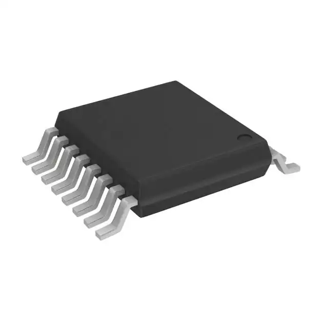
• Packaging (Pb-free & Green available)
– 16-pin 150-mil wide plastic QSOP (Q)
– 16-pin 173-mil wide plastic TSSOP (L)
The PI3L110 is fully specified for partial-power-down applications
using IOFF. The IOFF feature ensures that damaging current will
not backflow thoughout the device when it is powered down. The
device has isolation during Power Off.
Applications
• Dual Physical Layer Device sharing to one interface
connector
• Routes signals for 10/100 Mbit Ethernet
Pin Configuration
Block Diagram
IA0
IA1
IB0
IB1
IC0
IC1
ID0
ID1
S
1
16
IA0
2
15
3
14
4
13
5
12
6
11
7
10
8
9
IA1
E
YA
IB0
S
IB1
YB
GND
YA
YB
All trademarks are property of their respective owners.
YC
17-0005
VCC
E
ID0
ID1
YD
IC0
IC1
YC
YD
1
www.diodes.com 01/10/17
�A product Line of
Diodes Incorporated
PI3L110
Truth Table(1)
Pin Description
E
S
YA
YB
YC
YD
Function
H
X
Hi-Z
Hi-Z
Hi-Z
Hi-Z
Disable
L
L
IA 0
IB0
IC0
ID 0
S=0
L
H
IA 1
IB1
IC1
ID 1
S=1
Pin Name
IAN-IDN
S
E
YA-YD
GND
VCC
Note:
1. H = High Voltage Level
L = Low Voltage Level
X = Don't Care
Description
Data Inputs
Select Inputs
Enable
Data Outputs
Ground
Power
Maximum Ratings
(Above which useful life may be impaired. For user guidelines, not tested.)
Storage Temperature...................................................... –65°C to +150°C
Supply Voltage to Ground Potential
......................... –0.5V to +4.0V
DC Input Voltage.............................................................. –0.5V to +5.5V
DC Output Current......................................................................... 120mA
Power Dissipation............................................................................. 0.5W
Note: Stresses greater than those listed under MAXIMUM
RATINGS may cause permanent damage to the device. This
is a stress rating only and functional operation of the device
at these or any other conditions above those indicated in the
operational sections of this specification is not implied. Exposure to absolute maximum rating conditions for extended
periods may affect reliability.
DC Electrical Characteristics for 10/100 Base-T Ethernet Switching over Operating Range
(TA = –40°C to +85°C, VCC = 3.3V ±10%)
Parameter
Test Conditions(1)
Description
Min.
Typ.(2)
Max.
Units
0.8
V
VIH
Input HIGH Voltage
Guaranteed HIGH level
2.0
VIL
Input LOW Voltage
Guaranteed LOW level
–0.5
VIK
Clamp Diode Voltage
VCC = Max., IIN = –18mA
IIH
Input HIGH Current
VCC = Max., VIN = VCC
±5
µA
IIL
Input LOW Current
VCC = Max., VIN = GND
±5
µA
IOFF
Current while I/O disabled
VCC = 0, VO = 0 to 5V
1
µA
RON
Switch On-Resistance(3)
VCC = Min., 1.25V ≤ VIN ≤ VCC,
IIN = –10mA to –30mA
RFLAT(ON)
On-Resistance Flatness(4)
VCC = Min., VIN @ 1.25V and VCC,
IIN = –10mA to –30mA
∆RON
On-Resistance match from
center ports to any other port(4)
VCC = Min., 1.25V ≤ VIN ≤ VCC,
IIN = –10mA to –30mA
–0.7
4.0
–1.2
8.0
Ω
1
0.9
2.0
Notes:
1. For max. or min. conditions, use appropriate value specified under Electrical Characteristics for the applicable device type.
2. Typical values are at Vcc = 3.3V, Ta = 25°C ambient and maximum loading.
3. Measured by the voltage drop between IN and YN pins at indicated current through the switch. On-Resistance is determined by the lower of the
voltages on the two (IN & YN) pins.
4. This parameter is determined by device characterization but is not production tested.
All trademarks are property of their respective owners.
17-0005
2
www.diodes.com 01/10/17
�A product Line of
Diodes Incorporated
PI3L110
Capacitance (TA = 25°C, f = 1 MHz)
Parameters(1)
CIN
Description
Test Conditions
Typ.
Max.
2
3
4
6
9
10
Input Capacitance
COFF(In)
VIN = 0V
Port IN Capacitance, Switch OFF
CON
YN/IN Capacitance, Switch ON
Units
pF
Notes:
1. This parameter is determined by device characterization but is not production tested.
Power Supply Characteristics
Parameters
ICC
Test Conditions(1)
Description
Quiescent Power Supply Current
Min.
Typ.(2)
Max.
Units
800
µA
VCC = Max., VIN = GND or VCC
Notes:
1. For max. or min. conditions, use appropriate value specified under Electrical Characteristics for the applicable device type.
2. Typical values are at Vcc = 3.3V, Ta = 25°C ambient and maximum loading.
Dynamic Electrical Characteristics Over the Operating Range
(TA = –40°C to +85°C, Vcc = 3.3V ±10%, GND = 0V)
Parameter
XTALK
Description
Test Conditions
Crosstalk
OIRR
OFF Isolation
BW
Bandwidth –3dB
Min.
Typ.
–40
RL = 50Ω, f = 250 MHz
RL = 50Ω
350
tPD
Description
Propagation
Test Conditions
Min.
Delay(2,3)
MHz
Typ.(1)
Max.
Units
0.25
tPZH, tPZL
Line Enable Time - S or E to YN, IN
0.5
15
tPHZ, tPLZ
Line Disable Time - S to E to YN, IN
0.5
9
tSK(p)
Units
dB
–30
Characteristics
Paramenter
Max.
Skew between opposite transitions of the
same output (tPHL - tPLH) (2)
0.1
ns
0.2
Notes:
1. For max. or min. conditions, use appropriate value specified under Electrical Characteristics for the applicable device type.
2. Guaranteed by design.
3. The bus switch contributes no propagational delay other than the RC delay of the On-Resistance of the switch and the load capacitance. The
time constant for the switch alone is of the order of 0.25ns for 10pF load. Since this time constant is much smaller than the rise/fall times of
typical driving signals, it adds very little propagational delay to the system. Propagational delay of the bus switch when used in a system is
determined by the driving circuit on the driving side of the switch and its interactions with the load on the driven side.
All trademarks are property of their respective owners.
17-0005
3
www.diodes.com 01/10/17
�A product Line of
Diodes Incorporated
PI3L110
Test Circuit for Electrical Characteristics
6.0V
VCC
200-ohm
Pulse
Generator
VIN
D.U.T
VOUT
10pF
CL
RT
200-ohm
Notes:
• CL = Load capacitance: includes jig and probe capacitance.
• RT = Termination resistance: should be equal to ZOUT of the Pulse Generator
• Waveform 1 is for an output with internal conditions such that the output is low except when disabled by the output control.
• Waveform 2 is for an output with internal conditions such that the output is high except when disabled by the output control.
• All input impulses are supplied by generators having the following characteristics: PRR ≤ 10 MHz, ZO = 50Ω, tR ≤ 2.5ns, tF ≤ 2.5ns.
• The outputs are measured one at a time with one transition per measurement.
Switch Positions
Test
Switch
tPLZ, tPZL
6.0V
tPHZ, tPZH
GND
Prop Delay
Open
Test Circuit for Dynamic Electrical Characteristics
HP4195A
S1
VCC
T1
D.U.T
HP11667A
All trademarks are property of their respective owners.
R1
17-0005
10pF
4
50-ohm
www.diodes.com 01/10/17
�A product Line of
Diodes Incorporated
PI3L110
Switching Waveforms
2.5V
S or E
1.25V
1.25V
0V
3.5V
2.5V
Input
tPLH
Output
Output
2.5V
tPHL
tPLZ
VDD/2
1.5V
VOH
2.5V
tPZL
VOL
Output
VOL +0.3V
VOL
tPHZ
tPZH
2.5V
VOH
VDD/2
VOH -0.3V
VOH
VOL
Voltage Waveforms Enable and Disable Times
3.5V
2.5V
Input
tPLH
tPHL
1.5V
VOH
2.5V
Output
VOL
tSK(p) = I tPHL – tPLH I
Pulse Skew - tSK(p)
Applications Information
Logic Inputs
The logic control inputs can be driven up to +3.6V regardless of the supply voltage. For example, given a +3.3V supply, the output enables
or select pins may be driven low to 0V and high to 3.6V. Driving the control inputs Rail-to-Rail® minimizes power consumption.
Rail-to-Rail is a registered trademark of Nippon Motorola, Ltd.
All trademarks are property of their respective owners.
17-0005
5
www.diodes.com 01/10/17
�A product Line of
Diodes Incorporated
PI3L110
Packaging Mechanical: 16-Pin QSOP (Q)
16-0056
All trademarks are property of their respective owners.
17-0005
6
www.diodes.com 01/10/17
�A product Line of
Diodes Incorporated
PI3L110
Packaging Mechanical: 16-Pin TSSOP (L)
16-0061
Note: For latest package info, please check: http://www.pericom.com/support/packaging/packaging-mechanicals-and-thermal-characteristics/
Ordering Information
Ordering Code
Package Code
Package Description
PI3L110QE
Q
16-pin, 150-mil Wide (QSOP)
PI3L110QEX
Q
16-pin, 150-mil Wide (QSOP), Tape & Reel
PI3L110LE
L
16-pin, 173-mil Wide (TSSOP)
PI3L110LEX
L
16-pin, 173-mil Wide (TSSOP), Tape & Reel
Notes:
• Thermal characteristics can be found on the company web site at www.pericom.com/packaging/
• E = Pb-free & Green
• Adding an X suffix = Tape/Reel
All trademarks are property of their respective owners.
17-0005
7
www.diodes.com 01/10/17
�A product Line of
Diodes Incorporated
PI3L110
IMPORTANT NOTICE
DIODES INCORPORATED MAKES NO WARRANTY OF ANY KIND, EXPRESS OR IMPLIED, WITH REGARDS TO THIS DOCUMENT, INCLUDING, BUT NOT
LIMITED TO, THE IMPLIED WARRANTIES OF MERCHANTABILITY AND FITNESS FOR A PARTICULAR PURPOSE (AND THEIR EQUIVALENTS UNDER THE
LAWS OF ANY JURISDICTION).
Diodes Incorporated and its subsidiaries reserve the right to make modifications, enhancements, improvements, corrections or other changes without further notice
to this document and any product described herein. Diodes Incorporated does not assume any liability arising out of the application or use of this document or any
product described herein; neither does Diodes Incorporated convey any license under its patent or trademark rights, nor the rights of others. Any Customer or user of
this document or products described herein in such applications shall assume all risks of such use and will agree to hold Diodes Incorporated and all the companies
whose products are represented on Diodes Incorporated website, harmless against all damages.
Diodes Incorporated does not warrant or accept any liability whatsoever in respect of any products purchased through unauthorized sales channel.
Should Customers purchase or use Diodes Incorporated products for any unintended or unauthorized application, Customers shall indemnify and hold Diodes Incorporated and its representatives harmless against all claims, damages, expenses, and attorney fees arising out of, directly or indirectly, any claim of personal injury or
death associated with such unintended or unauthorized application.
Products described herein may be covered by one or more United States, international or foreign patents pending. Product names and markings noted herein may
also be covered by one or more United States, international or foreign trademarks.
This document is written in English but may be translated into multiple languages for reference. Only the English version of this document is the final and determinative format released by Diodes Incorporated.
LIFE SUPPORT
Diodes Incorporated products are specifically not authorized for use as critical components in life support devices or systems without the express written approval of
the Chief Executive Officer of Diodes Incorporated. As used herein:
A. Life support devices or systems are devices or systems which:
1. are intended to implant into the body, or
2. support or sustain life and whose failure to perform when properly used in accordance with instructions for use provided in the labeling can be reasonably expected
to result in significant injury to the user.
B. A critical component is any component in a life support device or system whose failure to perform can be reasonably expected to cause the
failure of the life support device or to affect its safety or effectiveness.
Customers represent that they have all necessary expertise in the safety and regulatory ramifications of their life support devices or systems, and acknowledge and
agree that they are solely responsible for all legal, regulatory and safety-related requirements concerning their products and any use of Diodes Incorporated products
in such safety-critical, life support devices or systems, notwithstanding any devices- or systems-related information or support that may be provided by Diodes Incorporated. Further, Customers must fully indemnify Diodes Incorporated and its representatives against any damages arising out of the use of Diodes Incorporated
products in such safety-critical, life support devices or systems.
Copyright © 2016, Diodes Incorporated
www.diodes.com
All trademarks are property of their respective owners.
17-0005
8
www.diodes.com 01/10/17
�


 工商网监
湘ICP备2023018690号
工商网监
湘ICP备2023018690号
