ZVP0120A
VGS=
-10V
-8V
-7V
-0.7
-0.6
ID(On) -On-State Drain Current (Amps)
ID(On) -On-State Drain Current (Amps)
TYPICAL CHARACTERISTICS
-0.5
-6V
-0.4
-0.3
-5V
-0.2
-4.5V
-0.1
-4V
0
-3.5V
0
-10 -20
-30 -40 -50 -60
-70 -80 -90 -100
-0.3
-14
-12
-10
-8
ID=
-300mA
-6
-4
-200mA
-2
-100mA
-50mA
0
0
-1
-2
-3
-4
-5
-6
-7
-8
-9
-10
ID(On)-On-State Drain Current (Amps)
VDS-Drain Source Voltage (Volts)
-16
-0.1
-4V
-3.5V
0
0
-1
-2
-3
-4
-5
-6
-7
-8
-9
-10
-1
-2
-3
-4 -5 -6 -7 -8 -9-10
Normalised RDS(on) and VGS(th)
-20
VGS-Gate Source Voltage (Volts)
On-resistance vs gate-source voltage
VALUE
UNIT
VDS
-200
V
-110
mA
-1
A
Saturation Characteristics
Gate Source Voltage
VGS
± 20
V
Power Dissipation at Tamb=25°C
Ptot
700
mW
Operating and Storage Temperature Range
Tj:Tstg
-55 to +150
°C
VDS=
-25V
ELECTRICAL CHARACTERISTICS (at Tamb = 25°C unless otherwise stated).
-0.5
-0.4
-10V
-0.3
-0.2
-0.1
0
0
-1
-2
-3
-4
-5
-6
-7
-8
-9
-10
2.4
2.2
2.0
e
nc
ta
sis
e
R
ce
ur
So
1.8
1.6
1.4
)
on
S(
RD
VGS=-10V
ID=-0.1A
ain
Dr
1.2
1.0
Gate Thresh
old
0.8
-40 -20
0
VGS=VDS
ID=-1mA
Voltage VGS
(th)
20 40 60 80 100 120 140 160 180
Temperature (°C)
Normalised RDS(on) and VGS(th) vs Temperature
3-407
SYMBOL
Drain-Source Voltage
IDM
-0.6
0.6
PARAMETER
ID
2.6
10
ABSOLUTE MAXIMUM RATINGS.
Pulsed Drain Current
VGS-Gate Source Voltage (Volts)
ID=
-300mA
-200mA
-I00mA
-50mA
E-Line
TO92 Compatible
Continuous Drain Current at Tamb=25°C
Transfer Characteristics
50
S
VDS - Drain Source Voltage (Volts)
-0.7
Voltage Saturation Characteristics
RDS(ON) -Drain Source Resistance (Ω)
D
G
-4.5V
VGS-Gate Source Voltage (Volts)
100
ISSUE 2 MARCH 94
FEATURES
* 200 Volt VDS
* RDS(on)=32Ω
-0.2
Output Characteristics
-18
ZVP0120A
-5V
VDS - Drain Source Voltage (Volts)
-20
VGS=
-10V
-8V
-7V
-6V
-0.4
P-CHANNEL ENHANCEMENT
MODE VERTICAL DMOS FET
PARAMETER
SYMBOL MIN. MAX. UNIT CONDITIONS.
Drain-Source
Breakdown Voltage
BVDSS
-200
Gate-Source
Threshold Voltage
VGS(th)
-1.5
Gate-Body Leakage
Zero Gate Voltage
Drain Current
V
ID=-1mA, VGS=0V
-3.5
V
ID=-1mA, VDS= VGS
IGSS
20
nA
VGS=± 20V, VDS=0V
IDSS
-10
-100
µA
µA
VDS=-200 V, VGS=0
VDS=-160 V, VGS=0V,
T=125°C(2)
On-State Drain Current(1)
ID(on)
Static Drain-Source On-State
Resistance (1)
RDS(on)
-250
Forward Transconductance
(1)(2)
gfs
Input Capacitance (2)
Ciss
100
pF
Common Source Output
Capacitance (2)
Coss
25
pF
Reverse Transfer Capacitance
(2)
Crss
7
pF
32
50
mA
VDS=-25 V, VGS=-10V
Ω
VGS=-10V,ID=-125mA
mS
VDS=-25V,ID=-125mA
Turn-On Delay Time (2)(3)
td(on)
7
ns
Rise Time (2)(3)
tr
15
ns
Turn-Off Delay Time (2)(3)
td(off)
12
ns
Fall Time (2)(3)
tf
15
ns
VDS=-25 V, VGS=0V, f=1MHz
VDD ≈− 25V, ID=-125mA
3-406
Measured under pulsed conditions. Width=300µs. Duty cycle ≤2% (2) Sample test.
(
1
)
�ZVP0120A
VGS=
-10V
-8V
-7V
-0.7
-0.6
ID(On) -On-State Drain Current (Amps)
ID(On) -On-State Drain Current (Amps)
TYPICAL CHARACTERISTICS
-0.5
-6V
-0.4
-0.3
-5V
-0.2
-4.5V
-0.1
-4V
0
-3.5V
0
-10 -20
-30 -40 -50 -60
-70 -80 -90 -100
-0.3
-14
-12
-10
-8
ID=
-300mA
-6
-4
-200mA
-2
-100mA
-50mA
0
0
-1
-2
-3
-4
-5
-6
-7
-8
-9
-10
ID(On)-On-State Drain Current (Amps)
VDS-Drain Source Voltage (Volts)
-16
-0.1
-4V
-3.5V
0
0
-1
-2
-3
-4
-5
-6
-7
-8
-9
-10
-1
-2
-3
-4 -5 -6 -7 -8 -9-10
Normalised RDS(on) and VGS(th)
-20
VGS-Gate Source Voltage (Volts)
On-resistance vs gate-source voltage
VALUE
UNIT
VDS
-200
V
-110
mA
-1
A
Saturation Characteristics
Gate Source Voltage
VGS
± 20
V
Power Dissipation at Tamb=25°C
Ptot
700
mW
Operating and Storage Temperature Range
Tj:Tstg
-55 to +150
°C
VDS=
-25V
ELECTRICAL CHARACTERISTICS (at Tamb = 25°C unless otherwise stated).
-0.5
-0.4
-10V
-0.3
-0.2
-0.1
0
0
-1
-2
-3
-4
-5
-6
-7
-8
-9
-10
2.4
2.2
2.0
e
nc
ta
sis
e
R
ce
ur
So
1.8
1.6
1.4
)
on
S(
RD
VGS=-10V
ID=-0.1A
ain
Dr
1.2
1.0
Gate Thresh
old
0.8
-40 -20
0
VGS=VDS
ID=-1mA
Voltage VGS
(th)
20 40 60 80 100 120 140 160 180
Temperature (°C)
Normalised RDS(on) and VGS(th) vs Temperature
3-407
SYMBOL
Drain-Source Voltage
IDM
-0.6
0.6
PARAMETER
ID
2.6
10
ABSOLUTE MAXIMUM RATINGS.
Pulsed Drain Current
VGS-Gate Source Voltage (Volts)
ID=
-300mA
-200mA
-I00mA
-50mA
E-Line
TO92 Compatible
Continuous Drain Current at Tamb=25°C
Transfer Characteristics
50
S
VDS - Drain Source Voltage (Volts)
-0.7
Voltage Saturation Characteristics
RDS(ON) -Drain Source Resistance (Ω)
D
G
-4.5V
VGS-Gate Source Voltage (Volts)
100
ISSUE 2 MARCH 94
FEATURES
* 200 Volt VDS
* RDS(on)=32Ω
-0.2
Output Characteristics
-18
ZVP0120A
-5V
VDS - Drain Source Voltage (Volts)
-20
VGS=
-10V
-8V
-7V
-6V
-0.4
P-CHANNEL ENHANCEMENT
MODE VERTICAL DMOS FET
PARAMETER
SYMBOL MIN. MAX. UNIT CONDITIONS.
Drain-Source
Breakdown Voltage
BVDSS
-200
Gate-Source
Threshold Voltage
VGS(th)
-1.5
Gate-Body Leakage
Zero Gate Voltage
Drain Current
V
ID=-1mA, VGS=0V
-3.5
V
ID=-1mA, VDS= VGS
IGSS
20
nA
VGS=± 20V, VDS=0V
IDSS
-10
-100
µA
µA
VDS=-200 V, VGS=0
VDS=-160 V, VGS=0V,
T=125°C(2)
On-State Drain Current(1)
ID(on)
Static Drain-Source On-State
Resistance (1)
RDS(on)
-250
Forward Transconductance
(1)(2)
gfs
Input Capacitance (2)
Ciss
100
pF
Common Source Output
Capacitance (2)
Coss
25
pF
Reverse Transfer Capacitance
(2)
Crss
7
pF
32
50
mA
VDS=-25 V, VGS=-10V
Ω
VGS=-10V,ID=-125mA
mS
VDS=-25V,ID=-125mA
Turn-On Delay Time (2)(3)
td(on)
7
ns
Rise Time (2)(3)
tr
15
ns
Turn-Off Delay Time (2)(3)
td(off)
12
ns
Fall Time (2)(3)
tf
15
ns
VDS=-25 V, VGS=0V, f=1MHz
VDD ≈− 25V, ID=-125mA
3-406
Measured under pulsed conditions. Width=300µs. Duty cycle ≤2% (2) Sample test.
(
1
)
�ZVP0120A
TYPICAL CHARACTERISTICS
gfs-Transconductance (mS)
gfs-Transconductance (mS)
200
180
VDS=-25V
160
140
120
100
80
60
40
20
0
0
-0.1
-0.2
-0.3 -0.4
-0.5
-0.6
-0.7
200
180
160
140
120
80
60
40
20
0
0
-0.8
Transconductance v drain current
90
80
70
Ciss
60
50
40
30
20
Coss
10
Crss
-30
-40
VGS-Gate Source Voltage (Volts)
C-Capacitance (pF)
100
-20
-2
-3
-4
-5
-6
-7
-8
-9
-10
Transconductance v gate-source voltage
110
-10
-1
VGS-Gate Source Voltage (Volts)
ID- Drain Current (Amps)
0
VDS=-25V
100
0
ID=- 0.4A
-2
-4
-6
VDS=
-50V -100V -180V
-8
-10
-12
-14
-16
0 0.2 0.4 0.6 0.8 1.0 1.2 1.4 1.6 1.8 2.0 2.2 2.4
-50
VDS-Drain Source Voltage (Volts)
Q-Charge (nC)
Capacitance v drain-source voltage
Gate charge v gate-source voltage
3-408
�
很抱歉,暂时无法提供与“ZVP0120ASTOA”相匹配的价格&库存,您可以联系我们找货
免费人工找货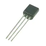


 工商网监
湘ICP备2023018690号
工商网监
湘ICP备2023018690号
