OBSOLETE - PLEASE USE ZXTD618MC
ZXTDBM832
MPPS™ Miniature Package Power Solutions
DUAL 20V NPN SILICON LOW SATURATION SWITCHING TRANSISTOR
SUMMARY
VCEO=20V; RSAT = 47m ; IC= 4.5A
DESCRIPTION
Packaged in the innovative 3mm x 2mm MLP (Micro Leaded Package) outline,
these new 4th generation low saturation dual transistors offer extremely low on
state losses making them ideal for use in DC-DC circuits and various driving
and power management functions.
Additionally users gain several other key benefits:
Performance capability equivalent to much larger packges
Improved circuit efficiency & power levels
3mm x 2mm (Dual die) MLP
PCB area and device placement savings
Lower package height (nom 0.9mm)
C1
C2
Reduced component count
FEATURES
• Low Equivalent On Resistance
B1
B2
• Extremely Low Saturation Voltage (150mV @1A)
• hFE characterised up to 6A
• IC=4.5A Continuous Collector Current
E2
• 3mm x 2mm MLP
E1
APPLICATIONS
• DC - DC Converters
• Charging circuits
• Power switches
PINOUT
• Motor control
ORDERING INFORMATION
DEVICE
REEL
TAPE
WIDTH
QUANTITY
PER REEL
ZXTDCM832TA
7 ⴕⴕ
8mm
3000
ZXTDCM832TC
13ⴕ ⴕ
8mm
10000
DEVICE MARKING
3mm x 2mm MLP
underside view
DBB
ISSUE 1 - JUNE 2002
1
�OBSOLETE - PLEASE USE ZXTD618MC
ZXTDBM832
ABSOLUTE MAXIMUM RATINGS.
PARAMETER
SYMBOL
LIMIT
UNIT
Collector-Base Voltage
V CBO
40
V
Collector-Emitter Voltage
V CEO
20
V
Emitter-Base Voltage
V EBO
7.5
V
Peak Pulse Current
I CM
12
A
Continuous Collector Current (a)(f)
IC
4.5
A
Continuous Collector Current (b)(f)
IC
5
A
Base Current
IB
1000
mA
Power Dissipation at TA=25°C (a)(f)
Linear Derating Factor
PD
1.5
12
W
mW/°C
Power Dissipation at TA=25°C (b)(f)
Linear Derating Factor
PD
2.45
19.6
W
mW/°C
Power Dissipation at TA=25°C (c)(f)
Linear Derating Factor
PD
1
8
W
mW/°C
Power Dissipation at TA=25°C (d)(f)
Linear Derating Factor
PD
1.13
9
W
mW/°C
Power Dissipation at TA=25°C (d)(g)
Linear Derating Factor
PD
1.7
13.6
W
mW/°C
Power Dissipation at TA=25°C (e)(g)
Linear Derating Factor
PD
3
24
W
mW/°C
Operating and Storage Temperature Range
T j :T stg
-55 to +150
°C
THERMAL RESISTANCE
PARAMETER
SYMBOL
VALUE
UNIT
Junction to Ambient (a)(f)
R θJA
83.3
°C/W
Junction to Ambient (b)(f)
R θJA
51
°C/W
Junction to Ambient (c)(f)
R θJA
125
°C/W
Junction to Ambient (d)(f)
R θJA
111
°C/W
Junction to Ambient (d)(g)
R θJA
73.5
°C/W
Junction to Ambient (e)(g)
R θJA
41.7
°C/W
Notes
(a) For a dual device surface mounted on 8 sq cm single sided 2oz copper on FR4 PCB, in still air conditions with all exposed pads attached. The
copper area is split down the centre line into two separate areas with one half connected to each half of the dual device.
(b) Measured at t
很抱歉,暂时无法提供与“ZXTDBM832TA”相匹配的价格&库存,您可以联系我们找货
免费人工找货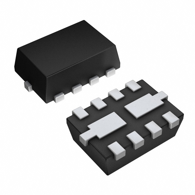


 工商网监
湘ICP备2023018690号
工商网监
湘ICP备2023018690号
