54ACT16952, 74ACT16952
16-BIT REGISTERED TRANSCEIVERS
WITH 3-STATE OUTPUTS
SCAS159C – JANUARY 1991 – REVISED APRIL 1996
D
D
D
D
D
D
D
D
D
Members of the Texas Instruments
Widebus Family
Inputs Are TTL-Voltage Compatible
Noninverting Outputs
Two 16-Bit, Back-to-Back Registers Store
Data Flowing in Both Directions
Flow-Through Architecture Optimizes
PCB Layout
Distributed VCC and GND Pin Configuration
Minimizes High-Speed Switching Noise
EPIC (Enhanced-Performance Implanted
CMOS) 1-µm Process
500-mA Typical Latch-Up Immunity at
125°C
Package Options Include Plastic 300-mil
Shrink Small-Outline (DL) Packages Using
25-mil Center-to-Center Pin Spacings and
380-mil Fine-Pitch Ceramic Flat (WD)
Packages Using 25-mil Center-to-Center
Pin Spacings
description
54ACT16952 . . . WD PACKAGE
74ACT16952 . . . DL PACKAGE
(TOP VIEW)
1OEAB
1CLKAB
1CEAB
GND
1A1
1A2
VCC
1A3
1A4
1A5
GND
1A6
1A7
1A8
2A1
2A2
2A3
GND
2A4
2A5
2A6
VCC
2A7
2A8
GND
2CEAB
2CLKAB
2OEAB
1
56
2
55
3
54
4
53
5
52
6
51
7
50
8
49
9
48
10
47
11
46
12
45
13
44
14
43
15
42
16
41
17
40
18
39
19
38
20
37
1OEBA
1CLKBA
1CEBA
GND
1B1
1B2
VCC
1B3
1B4
1B5
GND
1B6
1B7
1B8
2B1
2B2
2B3
GND
2B4
2B5
2B6
VCC
2B7
2B8
GND
2CEBA
2CLKBA
2OEBA
The ’ACT16952 are 16-bit registered transceivers
21
36
that contain two sets of D-type flip-flops for
22
35
temporary storage of data flowing in either
23
34
direction. They can be used as two 8-bit
24
33
transceivers or one 16-bit transceiver. Data on the
25
32
A or B bus is stored in registers on the low-to-high
26
31
transition of the clock (CLKAB or CLKBA) input,
27
30
provided that the clock-enable (CEAB or CEBA)
28
29
input is low. Taking the output-enable (OEAB or
OEBA) input low accesses the data on either port.
To avoid false clocking of the flip-flops, CEAB (or
CEBA) should not be switched from low to high
while CLKAB (or CLKBA) is low.
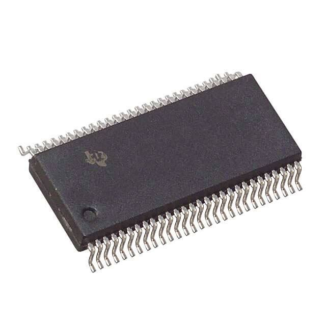
The 74ACT16952 is packaged in TI’s shrink small-outline package, which provides twice the I/O pin count and
functionality of standard small-outline packages in the same printed-circuit-board area.
The 54ACT16952 is characterized for operation over the full military temperature range of –55°C to 125°C. The
74ACT16952 is characterized for operation from –40°C to 85°C.
Please be aware that an important notice concerning availability, standard warranty, and use in critical applications of
Texas Instruments semiconductor products and disclaimers thereto appears at the end of this data sheet.
EPIC and Widebus are trademarks of Texas Instruments Incorporated.
Copyright 1996, Texas Instruments Incorporated
UNLESS OTHERWISE NOTED this document contains PRODUCTION
DATA information current as of publication date. Products conform to
specifications per the terms of Texas Instruments standard warranty.
Production processing does not necessarily include testing of all
parameters.
POST OFFICE BOX 655303
• DALLAS, TEXAS 75265
1
�54ACT16952, 74ACT16952
16-BIT REGISTERED TRANSCEIVERS
WITH 3-STATE OUTPUTS
SCAS159C – JANUARY 1991 – REVISED APRIL 1996
FUNCTION TABLE†
INPUTS
OUTPUT
B
CEAB
CLKAB
OEAB
A
H
X
L
X
X
H
L
X
L
↑
L
L
L
L
↑
L
H
H
B0‡
B0‡
X
X
H
X
Z
† A-to-B data flow is shown; B-to-A data flow is
similar but uses CEBA, CLKBA, and OEBA.
‡ Level of B before the indicated steady-state
input conditions were established
2
POST OFFICE BOX 655303
• DALLAS, TEXAS 75265
�54ACT16952, 74ACT16952
16-BIT REGISTERED TRANSCEIVERS
WITH 3-STATE OUTPUTS
SCAS159C – JANUARY 1991 – REVISED APRIL 1996
logic symbol†
1OEBA
56
54
1CEBA
1CLKBA
55
1
1OEAB
3
1CEAB
1CLKAB
2
29
2OEBA
31
2CEBA
2CLKBA
2OEAB
30
28
26
2CEAB
2CLKAB
1A1
27
5
EN3
G1
1C5
EN4
G2
2C6
EN9
G7
7C11
EN10
G8
8C12
3
6D
1A2
1A3
1A4
1A5
1A6
1A7
1A8
2A1
2A3
2A4
2A5
2A6
2A7
2A8
52
51
8
49
9
48
10
47
12
45
13
44
14
43
15
42
9
1B1
4
6
12D
2A2
5D
11D
1B2
1B3
1B4
1B5
1B6
1B7
1B8
2B1
10
16
41
17
40
19
38
20
37
21
36
23
34
24
33
2B2
2B3
2B4
2B5
2B6
2B7
2B8
† This symbol is in accordance with ANSI/IEEE Std 91-1984 and IEC Publication 617-12.
POST OFFICE BOX 655303
• DALLAS, TEXAS 75265
3
�54ACT16952, 74ACT16952
16-BIT REGISTERED TRANSCEIVERS
WITH 3-STATE OUTPUTS
SCAS159C – JANUARY 1991 – REVISED APRIL 1996
logic diagram (positive logic)
1OEBA
56
1CEBA
54
1CLKBA
55
1OEAB
1CEAB
1CLKAB
1A1
1
3
2
C1
5
1D
52
1B1
C1
1D
To Seven Other Channels
2OEBA
29
2CEBA
31
2CLKBA
30
2OEAB
2CEAB
2CLKAB
2A1
28
26
27
C1
15
1D
C1
1D
To Seven Other Channels
4
POST OFFICE BOX 655303
• DALLAS, TEXAS 75265
42
2B1
�54ACT16952, 74ACT16952
16-BIT REGISTERED TRANSCEIVERS
WITH 3-STATE OUTPUTS
SCAS159C – JANUARY 1991 – REVISED APRIL 1996
absolute maximum ratings over operating free-air temperature range (unless otherwise noted)†
Supply voltage range, VCC . . . . . . . . . . . . . . . . . . . . . . . . . . . . . . . . . . . . . . . . . . . . . . . . . . . . . . . . . . –0.5 V to 7 V
Input voltage range, VI (see Note 1) . . . . . . . . . . . . . . . . . . . . . . . . . . . . . . . . . . . . . . . . . . . –0.5 V to VCC + 0.5 V
Output voltage range, VO (see Note 1) . . . . . . . . . . . . . . . . . . . . . . . . . . . . . . . . . . . . . . . . –0.5 V to VCC + 0.5 V
Input clamp current, IIK (VI < 0 or VI > VCC) . . . . . . . . . . . . . . . . . . . . . . . . . . . . . . . . . . . . . . . . . . . . . . . . ±20 mA
Output clamp current, IOK (VO < 0 or VO > VCC) . . . . . . . . . . . . . . . . . . . . . . . . . . . . . . . . . . . . . . . . . . . . ±50 mA
Continuous output current, IO (VO = 0 to VCC) . . . . . . . . . . . . . . . . . . . . . . . . . . . . . . . . . . . . . . . . . . . . . . ±50 mA
Continuous current through VCC or GND . . . . . . . . . . . . . . . . . . . . . . . . . . . . . . . . . . . . . . . . . . . . . . . . . . ±400 mA
Maximum package power dissipation at TA = 55°C (in still air) (see Note 2): DL package . . . . . . . . . . . 1.4 W
Storage temperature range, Tstg . . . . . . . . . . . . . . . . . . . . . . . . . . . . . . . . . . . . . . . . . . . . . . . . . . . –65°C to 150°C
† Stresses beyond those listed under “absolute maximum ratings” may cause permanent damage to the device. These are stress ratings only, and
functional operation of the device at these or any other conditions beyond those indicated under “recommended operating conditions” is not
implied. Exposure to absolute-maximum-rated conditions for extended periods may affect device reliability.
NOTES: 1. The input and output voltage ratings may be exceeded if the input and output current ratings are observed.
2. The maximum package power dissipation is calculated using a junction temperature of 150_C and a board trace length of 750 mils.
recommended operating conditions (see Note 3)
54ACT16952
NOM
MAX
MIN
NOM
MAX
4.5
5
5.5
4.5
5
5.5
VCC
VIH
Supply voltage
VIL
VI
Low-level input voltage
Input voltage
0
VO
IOH
Output voltage
0
High-level output current
IOL
∆t/∆v
Low-level output current
High-level input voltage
74ACT16952
MIN
2
2
0.8
Input transition rise or fall rate
0
TA
Operating free-air temperature
–55
NOTE 3: Unused pins (input or I/O) must be held high or low to prevent them from floating.
UNIT
V
V
0.8
V
VCC
VCC
V
–24
–24
mA
24
24
mA
VCC
VCC
0
0
V
10
0
10
ns/V
125
–40
85
°C
PRODUCT PREVIEW information concerns products in the formative or
design phase of development. Characteristic data and other
specifications are design goals. Texas Instruments reserves the right to
change or discontinue these products without notice.
POST OFFICE BOX 655303
• DALLAS, TEXAS 75265
5
�54ACT16952, 74ACT16952
16-BIT REGISTERED TRANSCEIVERS
WITH 3-STATE OUTPUTS
SCAS159C – JANUARY 1991 – REVISED APRIL 1996
electrical characteristics over recommended operating free-air temperature range (unless
otherwise noted)
PARAMETER
TEST CONDITIONS
VCC
4.5 V
IOH = –50
50 µA
VOH
24 mA
IOH = –24
IOH = –50 mA†
IOH = –75 mA†
II
IOZ‡
A or B ports
ICC
∆ICC§
Ci
Control inputs
Cio
A or B ports
54ACT16952
MIN
MAX
74ACT16952
MIN
4.4
4.4
4.4
5.5 V
5.4
5.4
5.4
4.5 V
3.94
3.8
3.8
5.5 V
4.94
4.8
4.8
3.85
3.85
5.5 V
IOL = 24 mA
Control inputs
TA = 25°C
TYP
MAX
MAX
UNIT
V
5.5 V
IOL = 50 µA
VOL
MIN
4.5 V
0.1
0.1
5.5 V
0.1
0.1
0.1
0.1
4.5 V
0.36
0.44
0.44
5.5 V
0.36
0.44
0.44
1.65
1.65
V
IOL = 50 mA†
IOL = 75 mA†
5.5 V
VI = VCC or GND
VO = VCC or GND
5.5 V
±0.1
±1
±1
µA
5.5 V
±0.5
±5
±5
µA
VI = VCC or GND,
IO = 0
One input at 3.4 V,
Other inputs at VCC or GND
5.5 V
8
80
80
µA
5.5 V
0.9
1
1
mA
5.5 V
VI = VCC or GND
VO = VCC or GND
5V
3
pF
5V
12
pF
† Not more than one output should be tested at a time, and the duration of the test should not exceed 10 ms.
‡ For I/O ports, the parameter IOZ includes the input leakage current.
§ This is the increase in supply current for each input that is at one of the specified TTL voltage levels rather than 0 V or VCC.
timing requirements over recommended operating free-air temperature range,
VCC = 5 V ± 0.5 V (unless otherwise noted)
TA = 25°C
MIN
MAX
fclock
tw
Clock frequency
0
Pulse duration, CLK high or low
Set p time before CLK↑
Setup
th
Hold time after CLK↑
MAX
0
75
74ACT16952
MIN
MAX
0
75
6.7
6.7
5
5
5
6.5
6.5
6.5
Data
1
1
1
CEAB or CEBA
0
0
0
CEAB or CEBA
PRODUCT PREVIEW information concerns products in the formative or
design phase of development. Characteristic data and other
specifications are design goals. Texas Instruments reserves the right to
change or discontinue these products without notice.
6
MIN
6.7
Data
tsu
75
54ACT16952
POST OFFICE BOX 655303
• DALLAS, TEXAS 75265
UNIT
MHz
ns
ns
ns
�54ACT16952, 74ACT16952
16-BIT REGISTERED TRANSCEIVERS
WITH 3-STATE OUTPUTS
SCAS159C – JANUARY 1991 – REVISED APRIL 1996
switching characteristics over recommended operating free-air temperature range,
VCC = 5 V ± 0.5 V (unless otherwise noted) (see Figure 1)
PARAMETER
fmax
tPLH
tPHL
tPLH
tPHL
tPZH
tPZL
tPHZ
tPLZ
FROM
(INPUT)
TO
(OUTPUT)
MIN
TA = 25°C
TYP
MAX
75
CLK
A or B
CEBA or CEAB
A or B
OEBA or OEAB
A or B
OEBA or OEAB
A or B
54ACT16952
MIN
74ACT16952
MAX
MIN
75
MAX
75
UNIT
MHz
4.7
8.5
10.7
4.7
11.8
4.7
11.8
4.9
8.7
10.5
4.9
11.7
4.9
11.7
4.7
8.5
10.7
4.7
11.8
4.7
11.8
4.9
8.7
10.5
4.9
11.7
4.9
11.7
3.4
8.1
10.2
3.4
11.2
3.4
11.2
4.2
9.6
11.8
4.2
13
4.2
13
5.2
7.5
8.9
5.2
9.4
5.2
9.4
4.5
6.7
8.2
4.5
8.7
4.5
8.7
ns
ns
ns
ns
operating characteristics, VCC = 5 V, TA = 25°C
PARAMETER
Cpd
Power dissipation capacitance per transceiver
TEST CONDITIONS
Outputs enabled
CL = 50 pF,
f = 1 MHz
TYP
55
UNIT
pF
PRODUCT PREVIEW information concerns products in the formative or
design phase of development. Characteristic data and other
specifications are design goals. Texas Instruments reserves the right to
change or discontinue these products without notice.
POST OFFICE BOX 655303
• DALLAS, TEXAS 75265
7
�54ACT16952, 74ACT16952
16-BIT REGISTERED TRANSCEIVERS
WITH 3-STATE OUTPUTS
SCAS159C – JANUARY 1991 – REVISED APRIL 1996
PARAMETER MEASUREMENT INFORMATION
2 × VCC
S1
500 Ω
From Output
Under Test
Open
GND
TEST
S1
tPLH/tPHL
tPLZ/tPZL
tPHZ/tPZH
Open
2 × VCC
GND
500 Ω
CL = 50 pF
(see Note A)
LOAD CIRCUIT
3V
Timing Input
(see Note B)
1.5 V
0V
tw
tsu
3V
Input
1.5 V
1.5 V
th
3V
1.5 V
1.5 V
Data Input
0V
0V
VOLTAGE WAVEFORMS
VOLTAGE WAVEFORMS
3V
1.5 V
Input
1.5 V
0V
tPHL
tPLH
In-Phase
Output
50% VCC
VOH
50% VCC
VOL
50% VCC
VOH
50% VCC
VOL
3V
Output
Waveform 2
S1 at GND
(see Note B)
1.5 V
1.5 V
0V
tPZL
[ VCC
tPLZ
Output
Waveform 1
S1 at 2 × VCC
(see Note B)
tPLH
tPHL
Out-of-Phase
Output
Output
Control
(low-level
enabling)
50% VCC
VOL
tPHZ
tPZH
VOLTAGE WAVEFORMS
20% VCC
50% VCC
80% VCC
VOH
[0V
VOLTAGE WAVEFORMS
NOTES: A. CL includes probe and jig capacitance.
B. Waveform 1 is for an output with internal conditions such that the output is low except when disabled by the output control.
Waveform 2 is for an output with internal conditions such that the output is high except when disabled by the output control.
C. All input pulses are supplied by generators having the following characteristics: PRR ≤ 1 MHz, ZO = 50 Ω, tr = 3 ns, tf = 3 ns.
D. The outputs are measured one at a time with one input transition per measurement.
Figure 1. Load Circuit and Voltage Waveforms
8
POST OFFICE BOX 655303
• DALLAS, TEXAS 75265
�PACKAGE OPTION ADDENDUM
www.ti.com
1-Aug-2011
PACKAGING INFORMATION
Orderable Device
Status
(1)
Package Type Package
Drawing
Pins
Package Qty
Eco Plan
(2)
Lead/
Ball Finish
MSL Peak Temp
(3)
Samples
(Requires Login)
74ACT16952DL
ACTIVE
SSOP
DL
56
20
Green (RoHS
& no Sb/Br)
CU NIPDAU Level-1-260C-UNLIM
74ACT16952DLG4
ACTIVE
SSOP
DL
56
20
Green (RoHS
& no Sb/Br)
CU NIPDAU Level-1-260C-UNLIM
74ACT16952DLR
ACTIVE
SSOP
DL
56
TBD
Call TI
Call TI
74ACT16952DLRG4
ACTIVE
SSOP
DL
56
TBD
Call TI
Call TI
(1)
The marketing status values are defined as follows:
ACTIVE: Product device recommended for new designs.
LIFEBUY: TI has announced that the device will be discontinued, and a lifetime-buy period is in effect.
NRND: Not recommended for new designs. Device is in production to support existing customers, but TI does not recommend using this part in a new design.
PREVIEW: Device has been announced but is not in production. Samples may or may not be available.
OBSOLETE: TI has discontinued the production of the device.
(2)
Eco Plan - The planned eco-friendly classification: Pb-Free (RoHS), Pb-Free (RoHS Exempt), or Green (RoHS & no Sb/Br) - please check http://www.ti.com/productcontent for the latest availability
information and additional product content details.
TBD: The Pb-Free/Green conversion plan has not been defined.
Pb-Free (RoHS): TI's terms "Lead-Free" or "Pb-Free" mean semiconductor products that are compatible with the current RoHS requirements for all 6 substances, including the requirement that
lead not exceed 0.1% by weight in homogeneous materials. Where designed to be soldered at high temperatures, TI Pb-Free products are suitable for use in specified lead-free processes.
Pb-Free (RoHS Exempt): This component has a RoHS exemption for either 1) lead-based flip-chip solder bumps used between the die and package, or 2) lead-based die adhesive used between
the die and leadframe. The component is otherwise considered Pb-Free (RoHS compatible) as defined above.
Green (RoHS & no Sb/Br): TI defines "Green" to mean Pb-Free (RoHS compatible), and free of Bromine (Br) and Antimony (Sb) based flame retardants (Br or Sb do not exceed 0.1% by weight
in homogeneous material)
(3)
MSL, Peak Temp. -- The Moisture Sensitivity Level rating according to the JEDEC industry standard classifications, and peak solder temperature.
Important Information and Disclaimer:The information provided on this page represents TI's knowledge and belief as of the date that it is provided. TI bases its knowledge and belief on information
provided by third parties, and makes no representation or warranty as to the accuracy of such information. Efforts are underway to better integrate information from third parties. TI has taken and
continues to take reasonable steps to provide representative and accurate information but may not have conducted destructive testing or chemical analysis on incoming materials and chemicals.
TI and TI suppliers consider certain information to be proprietary, and thus CAS numbers and other limited information may not be available for release.
In no event shall TI's liability arising out of such information exceed the total purchase price of the TI part(s) at issue in this document sold by TI to Customer on an annual basis.
Addendum-Page 1
�IMPORTANT NOTICE
Texas Instruments Incorporated and its subsidiaries (TI) reserve the right to make corrections, modifications, enhancements, improvements,
and other changes to its products and services at any time and to discontinue any product or service without notice. Customers should
obtain the latest relevant information before placing orders and should verify that such information is current and complete. All products are
sold subject to TI’s terms and conditions of sale supplied at the time of order acknowledgment.
TI warrants performance of its hardware products to the specifications applicable at the time of sale in accordance with TI’s standard
warranty. Testing and other quality control techniques are used to the extent TI deems necessary to support this warranty. Except where
mandated by government requirements, testing of all parameters of each product is not necessarily performed.
TI assumes no liability for applications assistance or customer product design. Customers are responsible for their products and
applications using TI components. To minimize the risks associated with customer products and applications, customers should provide
adequate design and operating safeguards.
TI does not warrant or represent that any license, either express or implied, is granted under any TI patent right, copyright, mask work right,
or other TI intellectual property right relating to any combination, machine, or process in which TI products or services are used. Information
published by TI regarding third-party products or services does not constitute a license from TI to use such products or services or a
warranty or endorsement thereof. Use of such information may require a license from a third party under the patents or other intellectual
property of the third party, or a license from TI under the patents or other intellectual property of TI.
Reproduction of TI information in TI data books or data sheets is permissible only if reproduction is without alteration and is accompanied
by all associated warranties, conditions, limitations, and notices. Reproduction of this information with alteration is an unfair and deceptive
business practice. TI is not responsible or liable for such altered documentation. Information of third parties may be subject to additional
restrictions.
Resale of TI products or services with statements different from or beyond the parameters stated by TI for that product or service voids all
express and any implied warranties for the associated TI product or service and is an unfair and deceptive business practice. TI is not
responsible or liable for any such statements.
TI products are not authorized for use in safety-critical applications (such as life support) where a failure of the TI product would reasonably
be expected to cause severe personal injury or death, unless officers of the parties have executed an agreement specifically governing
such use. Buyers represent that they have all necessary expertise in the safety and regulatory ramifications of their applications, and
acknowledge and agree that they are solely responsible for all legal, regulatory and safety-related requirements concerning their products
and any use of TI products in such safety-critical applications, notwithstanding any applications-related information or support that may be
provided by TI. Further, Buyers must fully indemnify TI and its representatives against any damages arising out of the use of TI products in
such safety-critical applications.
TI products are neither designed nor intended for use in military/aerospace applications or environments unless the TI products are
specifically designated by TI as military-grade or "enhanced plastic." Only products designated by TI as military-grade meet military
specifications. Buyers acknowledge and agree that any such use of TI products which TI has not designated as military-grade is solely at
the Buyer's risk, and that they are solely responsible for compliance with all legal and regulatory requirements in connection with such use.
TI products are neither designed nor intended for use in automotive applications or environments unless the specific TI products are
designated by TI as compliant with ISO/TS 16949 requirements. Buyers acknowledge and agree that, if they use any non-designated
products in automotive applications, TI will not be responsible for any failure to meet such requirements.
Following are URLs where you can obtain information on other Texas Instruments products and application solutions:
Products
Applications
Audio
www.ti.com/audio
Communications and Telecom www.ti.com/communications
Amplifiers
amplifier.ti.com
Computers and Peripherals
www.ti.com/computers
Data Converters
dataconverter.ti.com
Consumer Electronics
www.ti.com/consumer-apps
DLP® Products
www.dlp.com
Energy and Lighting
www.ti.com/energy
DSP
dsp.ti.com
Industrial
www.ti.com/industrial
Clocks and Timers
www.ti.com/clocks
Medical
www.ti.com/medical
Interface
interface.ti.com
Security
www.ti.com/security
Logic
logic.ti.com
Space, Avionics and Defense
www.ti.com/space-avionics-defense
Power Mgmt
power.ti.com
Transportation and
Automotive
www.ti.com/automotive
Microcontrollers
microcontroller.ti.com
Video and Imaging
www.ti.com/video
RFID
www.ti-rfid.com
Wireless
www.ti.com/wireless-apps
RF/IF and ZigBee® Solutions
www.ti.com/lprf
TI E2E Community Home Page
e2e.ti.com
Mailing Address: Texas Instruments, Post Office Box 655303, Dallas, Texas 75265
Copyright © 2011, Texas Instruments Incorporated
�


 工商网监
湘ICP备2023018690号
工商网监
湘ICP备2023018690号
