SN74HSTL16919
9-BIT TO 18-BIT HSTL-TO-LVTTL MEMORY ADDRESS LATCH
WITH INPUT PULLUP RESISTORS
SCES348 – MARCH 2001
D
D
D
D
D
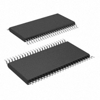
DGG PACKAGE
(TOP VIEW)
Member of Texas Instruments’ Widebus
Family
Inputs Meet JEDEC HSTL Std JESD 8-6,
and Outputs Meet Level III Specifications
10-kΩ Pullup Resistor on Data and LE
Inputs
Latch-Up Performance Exceeds 100 mA Per
JESD 78, Class II
ESD Protection Exceeds JESD 22
– 2000-V Human-Body Model (A114-A)
– 200-V Machine Model (A115-A)
– 1000-V Charged-Device Model (C101)
2Q1
1Q1
GND
D1
D2
VCC
D3
D4
GND
1LE
GND
VREF
GND
2LE
GND
D5
D6
D7
VCC
D8
D9
GND
2Q9
1Q9
description
This 9-bit to 18-bit D-type latch is designed for
3.15-V to 3.45-V VCC operation. The D inputs
accept HSTL levels and the Q outputs provide
LVTTL levels.
The SN74HSTL16919 is particularly suitable for
driving an address bus to two banks of memory.
Each bank of nine outputs is controlled with its
own latch-enable (LE) input.
Each of the nine D inputs is tied to the inputs of two
D-type latches that provide true data (Q) at the
outputs. While LE is low, the Q outputs of the
corresponding nine latches follow the D inputs.
When LE is taken high, the Q outputs are latched
at the levels set up at the D inputs.
1
48
2
47
3
46
4
45
5
44
6
43
7
42
8
41
9
40
10
39
11
38
12
37
13
36
14
35
15
34
16
33
17
32
18
31
19
30
20
29
21
28
22
27
23
26
24
25
VCC
VCC
1Q2
2Q2
GND
1Q3
2Q3
VCC
1Q4
2Q4
GND
1Q5
2Q5
GND
1Q6
2Q6
VCC
1Q7
2Q7
GND
1Q8
2Q8
VCC
VCC
To ensure low ICC during power up or power down, 10-kΩ pullup resistors are included on the D and LE inputs
to ensure a differential voltage relative to VREF. VREF must be applied prior to or at the same time as VCC, or
VREF must be pulled down to ground.
ORDERING INFORMATION
TA
PACKAGE†
ORDERABLE
PART NUMBER
TOP-SIDE
MARKING
0°C to 70°C
TSSOP – DGG Tape and reel
SN74HSTL16919DGGR
HSTL16919
† Package drawings, standard packing quantities, thermal data, symbolization, and PCB design
guidelines are available at www.ti.com/sc/package.
Please be aware that an important notice concerning availability, standard warranty, and use in critical applications of
Texas Instruments semiconductor products and disclaimers thereto appears at the end of this data sheet.
Widebus is a trademark of Texas Instruments.
Copyright 2001, Texas Instruments Incorporated
PRODUCTION DATA information is current as of publication date.
Products conform to specifications per the terms of Texas Instruments
standard warranty. Production processing does not necessarily include
testing of all parameters.
POST OFFICE BOX 655303
• DALLAS, TEXAS 75265
1
�SN74HSTL16919
9-BIT TO 18-BIT HSTL-TO-LVTTL MEMORY ADDRESS LATCH
WITH INPUT PULLUP RESISTORS
SCES348 – MARCH 2001
FUNCTION TABLE
INPUTS
LE
D
OUTPUT
Q
L
H
H
L
L
H
X
L
Q0†
† Output level before the
indicated steady-state input
conditions were established
logic diagram (positive logic)
12
VREF
10
1LE
D1
4
1D
2
1Q1
C1
14
1D
2LE
1
2Q1
C1
To Eight Other Channels
absolute maximum ratings over operating free-air temperature range (unless otherwise noted)‡
Supply voltage range, VCC . . . . . . . . . . . . . . . . . . . . . . . . . . . . . . . . . . . . . . . . . . . . . . . . . . . . . . . . . –0.5 V to 4.6 V
Input voltage range, VI (see Note 1) . . . . . . . . . . . . . . . . . . . . . . . . . . . . . . . . . . . . . . . . . . . –0.5 V to VCC + 0.5 V
Output voltage range, VO (see Note 1) . . . . . . . . . . . . . . . . . . . . . . . . . . . . . . . . . . . . . . . . –0.5 V to VCC + 0.5 V
Input clamp current, IIK (VI < 0) . . . . . . . . . . . . . . . . . . . . . . . . . . . . . . . . . . . . . . . . . . . . . . . . . . . . . . . . . . . –50 mA
Output clamp current, IOK (VO < 0 or VO > VCC) . . . . . . . . . . . . . . . . . . . . . . . . . . . . . . . . . . . . . . . . . . . . ±50 mA
Continuous output current, IO (VO = 0 to VCC) . . . . . . . . . . . . . . . . . . . . . . . . . . . . . . . . . . . . . . . . . . . . . . ±50 mA
Continuous current through each VCC or GND . . . . . . . . . . . . . . . . . . . . . . . . . . . . . . . . . . . . . . . . . . . . . ±100 mA
Package thermal impedance, θJA (see Note 2) . . . . . . . . . . . . . . . . . . . . . . . . . . . . . . . . . . . . . . . . . . . . . 89°C/W
Storage temperature range, Tstg . . . . . . . . . . . . . . . . . . . . . . . . . . . . . . . . . . . . . . . . . . . . . . . . . . . –65°C to 150°C
‡ Stresses beyond those listed under “absolute maximum ratings” may cause permanent damage to the device. These are stress ratings only, and
functional operation of the device at these or any other conditions beyond those indicated under “recommended operating conditions” is not
implied. Exposure to absolute-maximum-rated conditions for extended periods may affect device reliability.
NOTES: 1. The input and output negative-voltage ratings may be exceeded if the input and output clamp-current ratings are observed.
2. The package thermal impedance is calculated in accordance with JESD 51-7.
2
POST OFFICE BOX 655303
• DALLAS, TEXAS 75265
�SN74HSTL16919
9-BIT TO 18-BIT HSTL-TO-LVTTL MEMORY ADDRESS LATCH
WITH INPUT PULLUP RESISTORS
SCES348 – MARCH 2001
recommended operating conditions (see Note 3)
MIN
VCC
VREF
Supply voltage
3.15
Reference voltage
0.68
VI
VIH
Input voltage
AC high-level input voltage
All inputs
VIL
VIH
AC low-level input voltage
All inputs
DC high-level input voltage
All inputs
VIL
IOH
DC low-level input voltage
All inputs
IOL
TA
Low-level output current
NOM
MAX
UNIT
3.45
V
0.9
V
1.5
V
0.75
0
VREF+200 mV
V
VREF–200 mV
VREF+100 mV
V
VREF–100 mV
–24
High-level output current
Operating free-air temperature
V
0
V
mA
24
mA
70
°C
NOTE 3: All unused inputs of the device must maintain a minimum differential voltage of 100 mV between data inputs and VREF to ensure proper
device operation. Refer to the TI application report, Implications of Slow or Floating CMOS Inputs, literature number SCBA004.
electrical characteristics over recommended operating free-air temperature range (unless
otherwise noted)
PARAMETER
TEST CONDITIONS
VIK
VOH
VCC = 3.15 V,
VCC = 3.15 V,
II = –18 mA
IOH = –24 mA
VOL
VCC = 3.15 V,
IOL = 24 mA
VI = 0 or 1.5 V
Control inputs
II
Data inputs
VCC = 3.45 V
VREF
ICC
Ci
Control inputs
Data inputs
TYP†
VI = 0 or 1.5 V
VI = 0 or 3.3 V
VCC = 0 or 3.3 V,
VCC = 0,
VI = 0 or 3.3 V
VO = 0
MAX
UNIT
–1.2
V
2.4
V
0.5
V
–500
VI = 0 or 1.5 V
VREF = 0.68 V or 0.9 V
VCC = 3.45 V,
VCC = 0 or 3.3 V,
Co
Outputs
† All typical values are at VCC = 3.3 V, TA = 25°C.
MIN
–500
µA
90
50
100
2.5
mA
pF
2.5
2.5
pF
timing requirements over recommended ranges of supply voltage and operating free-air
temperature (unless otherwise noted) (see Figure 1)
VCC = 3.3 V
± 0.15 V
MIN
tw
tsu
Pulse duration, LE low
th
tldr‡
Hold time
Setup time, D before LE↑
D after LE↑
UNIT
MAX
3
ns
2
ns
1
ns
Data race condition time
D after LE↓
0
ns
‡ This is the maximum time after LE switches low that the data input can return to the latched state from the opposite state without producing a
glitch on the output.
POST OFFICE BOX 655303
• DALLAS, TEXAS 75265
3
�SN74HSTL16919
9-BIT TO 18-BIT HSTL-TO-LVTTL MEMORY ADDRESS LATCH
WITH INPUT PULLUP RESISTORS
SCES348 – MARCH 2001
switching characteristics over recommended operating free-air temperature range, VREF = 0.75 V
PARAMETER
tpd
d
FROM
(INPUT)
TO
(OUTPUT)
D
Q
LE
VCC = 3.3 V
± 0.15 V
MIN
MAX
1.9
3.5
1.9
4.3
UNIT
ns
simultaneous switching characteristics over recommended operating free-air temperature range,
VREF = 0.75 V†
PARAMETER
tpd
d
FROM
(INPUT)
TO
(OUTPUT)
D
Q
LE
† All outputs switching.
4
POST OFFICE BOX 655303
• DALLAS, TEXAS 75265
VCC = 3.3 V
± 0.15 V
MIN
MAX
1.9
4.5
1.9
5.3
UNIT
ns
�SN74HSTL16919
9-BIT TO 18-BIT HSTL-TO-LVTTL MEMORY ADDRESS LATCH
WITH INPUT PULLUP RESISTORS
SCES348 – MARCH 2001
PARAMETER MEASUREMENT INFORMATION
1.25 V
VREF
LE
0.25 V
From Output
Under Test
CL = 80 pF
(see Note A)
tsu
500 Ω
th
1.25 V
Data Input
VREF
VREF
0.25 V
LOAD CIRCUIT
VOLTAGE WAVEFORMS
SETUP AND HOLD TIMES
Input
(see Note B)
1.25 V
VREF
VREF
0.25 V
tPLH
tw
tPHL
1.25 V
Input
VREF
VREF
VOH
Output
1.5 V
0.25 V
VOL
VOLTAGE WAVEFORMS
PULSE DURATION
NOTES: A.
B.
C.
D.
1.5 V
VOLTAGE WAVEFORMS
PROPAGATION DELAY TIMES
CL includes probe and jig capacitance.
All input pulses are supplied by generators having the following characteristics: PRR ≤ 10 MHz, ZO = 50 Ω, tr ≤ 1 ns, tf ≤ 1 ns.
The outputs are measured one at a time with one transition per measurement.
tPHL and tPLH are the same as tpd.
Figure 1. Load Circuit and Voltage Waveforms
POST OFFICE BOX 655303
• DALLAS, TEXAS 75265
5
�IMPORTANT NOTICE
Texas Instruments and its subsidiaries (TI) reserve the right to make changes to their products or to discontinue
any product or service without notice, and advise customers to obtain the latest version of relevant information
to verify, before placing orders, that information being relied on is current and complete. All products are sold
subject to the terms and conditions of sale supplied at the time of order acknowledgment, including those
pertaining to warranty, patent infringement, and limitation of liability.
TI warrants performance of its products to the specifications applicable at the time of sale in accordance with
TI’s standard warranty. Testing and other quality control techniques are utilized to the extent TI deems necessary
to support this warranty. Specific testing of all parameters of each device is not necessarily performed, except
those mandated by government requirements.
Customers are responsible for their applications using TI components.
In order to minimize risks associated with the customer’s applications, adequate design and operating
safeguards must be provided by the customer to minimize inherent or procedural hazards.
TI assumes no liability for applications assistance or customer product design. TI does not warrant or represent
that any license, either express or implied, is granted under any patent right, copyright, mask work right, or other
intellectual property right of TI covering or relating to any combination, machine, or process in which such
products or services might be or are used. TI’s publication of information regarding any third party’s products
or services does not constitute TI’s approval, license, warranty or endorsement thereof.
Reproduction of information in TI data books or data sheets is permissible only if reproduction is without
alteration and is accompanied by all associated warranties, conditions, limitations and notices. Representation
or reproduction of this information with alteration voids all warranties provided for an associated TI product or
service, is an unfair and deceptive business practice, and TI is not responsible nor liable for any such use.
Resale of TI’s products or services with statements different from or beyond the parameters stated by TI for
that product or service voids all express and any implied warranties for the associated TI product or service,
is an unfair and deceptive business practice, and TI is not responsible nor liable for any such use.
Also see: Standard Terms and Conditions of Sale for Semiconductor Products. www.ti.com/sc/docs/stdterms.htm
Mailing Address:
Texas Instruments
Post Office Box 655303
Dallas, Texas 75265
Copyright 2001, Texas Instruments Incorporated
�


 工商网监
湘ICP备2023018690号
工商网监
湘ICP备2023018690号
