ADC16V130
www.ti.com
SNAS458E – NOVEMBER 2008 – REVISED MARCH 2013
ADC16V130 16-Bit, 130 MSPS A/D Converter With LVDS Outputs
Check for Samples: ADC16V130
FEATURES
APPLICATIONS
•
•
•
•
1
2
•
•
•
•
•
•
•
•
Dual Supplies: 1.8V and 3.0V Operation
On Chip Automatic Calibration During PowerUp
Low Power Consumption
Multi-Level Multi-Function Pins for CLK/DF and
PD
Power-Down and Sleep Modes
On Chip Precision Reference and Sample-andHold Circuit
On Chip Low Jitter Duty-Cycle Stabilizer
Offset Binary or 2's Complement Data Format
Full Data Rate LVDS Output Port
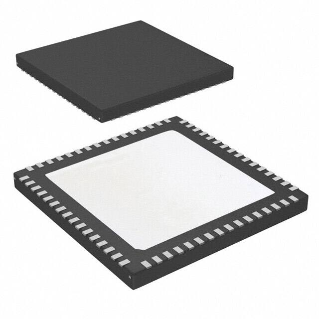
64-pin WQFN Package (9x9x0.8, 0.5mm PinPitch)
KEY SPECIFICATIONS
•
•
•
•
•
•
•
Resolution: 16 Bits
Conversion Rate: 130 MSPS
SNR
– (fIN = 10MHz): 78.5 dBFS (Typ)
– (fIN = 70MHz): 77.8 dBFS (Typ)
– (fIN = 160MHz): 76.7 dBFS (Typ)
SFDR
– (fIN = 10MHz): 95.5 dBFS (Typ)
– (fIN = 70MHz): 92.0 dBFS (Typ)
– (fIN = 160MHz): 90.6 dBFS (Typ)
Full Power Bandwidth: 1.4 GHz (Typ)
Power Consumption
– Core: 650 mW (Typ)
– LVDS Driver: 105 mW (Typ)
– Total: 755 mW (Typ)
Operating Temperature Range: -40°C ~ 85°C
•
•
•
•
High IF Sampling Receivers
Multi-carrier Base Station Receivers
– GSM/EDGE, CDMA2000, UMTS, LTE, and
WiMax
Test and Measurement Equipment
Communications Instrumentation
Data Acquisition
Portable Instrumentation
DESCRIPTION
The ADC16V130 is a monolithic high performance
CMOS analog-to-digital converter capable of
converting analog input signals into 16-bit digital
words at rates up to 130 Mega Samples Per Second
(MSPS). This converter uses a differential, pipelined
architecture with digital error correction and an onchip sample-and-hold circuit to minimize power
consumption and external component count while
providing excellent dynamic performance. Automatic
power-up calibration enables excellent dynamic
performance and reduces part-to-part variation, and
the ADC16V130 could be re-calibrated at any time by
asserting and then de-asserting power-down. An
integrated low noise and stable voltage reference and
differential reference buffer amplifier easies board
level design. On-chip duty cycle stabilizer with low
additive jitter allows wide duty cycle range of input
clock without compromising its dynamic performance.
A unique sample-and-hold stage yields a full-power
bandwidth of 1.4 GHz. The digital data is provided via
full data rate LVDS outputs – making possible the 64pin, 9mm x 9mm WQFN package. The ADC16V130
operates on dual power supplies +1.8V and +3.0V
with a power-down feature to reduce the power
consumption to very low levels while allowing fast
recovery to full operation.
1
2
Please be aware that an important notice concerning availability, standard warranty, and use in critical applications of
Texas Instruments semiconductor products and disclaimers thereto appears at the end of this data sheet.
All trademarks are the property of their respective owners.
PRODUCTION DATA information is current as of publication date.
Products conform to specifications per the terms of the Texas
Instruments standard warranty. Production processing does not
necessarily include testing of all parameters.
Copyright © 2008–2013, Texas Instruments Incorporated
�ADC16V130
SNAS458E – NOVEMBER 2008 – REVISED MARCH 2013
www.ti.com
Block Diagram
CLK+
DUTY CYCLE
STABILIZER
CLK-
34
VIN+
16BIT HIGH SPEED
PIPELINE ADC
SHA
VIN-
ERROR CORRECTION
LOGIC
SDR LVDS
BUFFER
2
DO+/-, OR+/OUTCLK+/-
VRN
VRM
VRP
INTERNAL
REFERENCE
MULTI-LEVEL
FUNCTION
PD
CLK/DF
VREF
CALIBRATION ENGINE
CLK_SEL/DF
2
VA1.8
AGND
VIN-
VIN+
AGND
VA3.0
VRM
VREF
AGND
VA3.0
OR+
OR-
D15+
D15-
D14+
D14-
64
63
62
61
60
59
58
57
56
55
54
53
52
51
50
49
Connection Diagram
1
EXPOSED PADDLE ON BOTTOM
OF PACKAGE, PIN 0
48
D13+
47
D13-
VA3.0
2
AGND
3
46
D12+
VRN
4
45
D12-
VRN
5
44
VDR
VRP
6
43
DRGND
VRP
7
42
D11+
AGND
8
41
D11-
VA1.8
9
40
D10+
CLK+
ADC16V130
(Top View)
28
29
30
31
32
D6-
D6+
D7-
D7+
OUTCLK-
D5+
33
27
16
26
DO+
D5-
OUTCLK+
25
34
D4-
15
D4+
DO-
24
D8-
VDR
35
23
14
22
D8+
D3+
36
DRGND
13
PD
21
VAD1.8
D3-
D9-
20
37
19
12
D2-
AGND
D2+
D9+
18
11
D1+
D10-
38
17
39
D1-
10
CLK-
Submit Documentation Feedback
Copyright © 2008–2013, Texas Instruments Incorporated
Product Folder Links: ADC16V130
�ADC16V130
www.ti.com
SNAS458E – NOVEMBER 2008 – REVISED MARCH 2013
PIN DESCRIPTIONS
Pin No.
Symbol
Equivalent Circuit
Function and Connection
ANALOG I/O
61
VIN+
VA3.0
62
Differential analog input pins. The differential full-scale input signal
level is 2.4Vpp as default. Each input pin signal centered on a
common mode voltage, VCM.
VIN-
AGND
6,7
Upper reference voltage.
This pin should not be used to source or sink current. The decoupling
capacitor to AGND (low ESL 0.1μF) should be placed very close to
the pin to minimize stray inductance. VRP needs to be connected to
VRN through a low ESL 0.1μF and a low ESR 10μF capacitors in
parallel.
VRP
VA3.0
VRM
VA3.0
4,5
VRN
VRN
VREF
VA3.0
58
VRP
VRM
AGND
IDC
VREF
AGND
CLK+
VA3.0
CLK−
10 k:
11
VA3.0
VA1.8
10 k:
10
Common mode voltage
The decoupling capacitor to AGND (low ESL 0.1μF) should be placed
as close to the pin as possible to minimize stray inductance. It is
recommended to use VRM to provide the common mode voltage for
the differential analog inputs.
Internal reference voltage output / External reference voltage input.
By default, this pin is the output for the internal 1.2V voltage
reference. This pin should not be used to sink or source current and
should be decoupled to AGND with a 0.1μF, low ESL capacitor. The
decoupling capacitors should be placed as close to the pins as
possible to minimize inductance and optimize ADC performance. The
size of decoupling capacitor should not be larger than 0.1μF,
otherwise dynamic performance after power-up calibration can drop
due to the long VREF settling.
This pin can also be used as the input for a low noise external
reference voltage. The output impedance for the internal reference at
this pin is 9 kΩ and this can be overdriven provided the impedance of
the external source is 9 kΩ and can be easily
over-driven by external reference. Two multi-level multi-function pins can program data format, clock mode,
power down and sleep mode.
ADC Architecture
The ADC16V130 architecture consists of a highly linear and wide bandwidth sample-and-hold circuit, followed by
a switched capacitor pipeline ADC. Each stage of the pipeline ADC consists of low resolution flash sub-ADC and
an inter-stage multiplying digital-to-analog converter (MDAC), which is a switched capacitor amplifier with a fixed
stage signal gain and DC level shifting circuits. The amount of DC level shifting is dependent on sub-ADC digital
output code. 16bit final digital output is the result of the digital error correction logic, which receives digital output
of each stage including redundant bits to correct offset error of each sub-ADC.
APPLICATIONS INFORMATION
OPERATING CONDITIONS
We recommend that the following conditions be observed for operation of the ADC16V130:
2.7V ≤ VA3.0 ≤ 3.6V
1.7V ≤ VA1.8 ≤ 1.9V
1.7V ≤ VAD1.8 ≤ 1.9V
1.7V ≤ VDR ≤ 1.9V
5 MSPS ≤ FCLK ≤ 130 MSPS
VREF ≤ 1.2V
VCM = 1.15V (from VRM)
ANALOG INPUTS
Analog input circuit of the ADC16V130 is a differential switched capacitor sample-and-hold circuit (see Figure 20)
that provides optimum dynamic performance wide input frequency range with minimum power consumption. The
clock signal alternates sample mode (QS) and hold mode (QH). An integrated low jitter duty cycle stabilizer
ensures constant optimal sample and hold time over wide range of input clock duty cycle. The duty cycle
stabilizer is always turned on during normal operation.
During sample mode, analog signals (VIN+, VIN-) are sampled across two sampling capacitor (CS) while the
amplifier in the sample-and-hold circuit is idle. The dynamic performance of the ADC16V130 is likely determined
during sampling mode. The sampled analog inputs (VIN+, VIN-) are held during hold mode by connecting input
side of the sampling capacitors to output of the amplifier in the sample-and-hold circuit while driving pipeline ADC
core.
The signal source, which drives the ADC16V130, is recommended to have source impedance less than 100 Ω
over wide frequency range for optimal dynamic performance.
A shunt capacitor can be placed across the inputs to provide high frequency dynamic charging current during
sample mode and also absorb any switching charge coming from the ADC16V130. A shunt capacitor can be
placed across each input to GND for similar purpose. Smaller physical size and low ESR and ESL shunt
capacitor is recommended.
The value of shunt capacitor should be carefully chosen to optimize the dynamic performance at certain input
frequency range. Larger value shunt capacitors can be used for low input frequency range, but the value has to
be reduced at high input frequency range.
Balancing impedance at positive and negative input pin over entire signal path must be ensured for optimal
dynamic performance.
Submit Documentation Feedback
Copyright © 2008–2013, Texas Instruments Incorporated
Product Folder Links: ADC16V130
15
�ADC16V130
SNAS458E – NOVEMBER 2008 – REVISED MARCH 2013
www.ti.com
QH
CS
VIN+
-
+
+
-
QS
QS
CS
VIN -
QH
Figure 20. Simplified Switched-Capacitor Sample-and-hold Circuit
Input Common Mode
The analog inputs of the ADC16V130 are not internally dc biased and the range of input common mode is very
narrow. Hence it is highly recommended to use the common mode voltage (VRM, typically 1.15V) as input
common mode for optimal dynamic performance regardless of DC and AC coupling applications. Input common
mode signal must be decoupled with low ESL 0.1μF at the far end of load point to minimize noise performance
degradation due to any coupling or switching noise between the ADC16V130 and input driving circuit.
Driving Analog Inputs
For low frequency applications, either a flux or balun transformer can convert single-ended input signal into
differential and drive the ADC16V130 without additive noise. An example is shown in Figure 21. VRM pin is used
to bias the input common mode by connecting the center tap of the transformer’s secondary ports. Flux
transformer is used for this example, but AC coupling capacitors should be added once balun type transformer is
used.
VIN +
R
C
R
ADC16V130
VIN -
VRM
0.1 PF
Figure 21. Transformer Drive Circuit for Low Input Frequency
Transformer has a characteristic of band pass filtering. It sets lower band limit by being saturated at frequencies
below a few MHz and sets upper frequency limit due to its parasitic resistance and capacitance. The transformer
core will be saturated with excessive signal power and it causes distortion as equivalent load termination
becomes heavier at high input frequencies. This is a reason to reduce shunt capacitors for high IF sampling
application to balance the amount of distortion caused by transformer and charge kick-back noise from the
device.
As input frequency goes higher with the input network in Figure 22, amplitude and phase unbalance increase
between positive and negative inputs (VIN+ and VIN-) due to the inherent impedance mismatch between the two
primary ports of the transformer while one is connected to the signal source and the other is connected to GND.
Distortion increases as the result.
16
Submit Documentation Feedback
Copyright © 2008–2013, Texas Instruments Incorporated
Product Folder Links: ADC16V130
�ADC16V130
www.ti.com
SNAS458E – NOVEMBER 2008 – REVISED MARCH 2013
Cascaded transmission line transformers can be used for high frequency applications like high IF sampling base
station receiver channel. Transmission line transformer has less stray capacitance between primary and
secondary ports and so the amount of impedance at secondary ports is effectively less even with the given
inherent impedance mismatch on the primary ports. Cascading two transmission line transformers further
reduces the effective stray capacitance from the secondary of ports of the secondary transformer to primary ports
of first transformer, where impedance is mismatched. A transmission line transformer, for instance MABACT0040
from M/A-COM, with center tap on secondary port could further reduce amplitude and phase mismatch.
0.1 PF
R
VIN +
C1
C2
ADC16V130
0.1 PF
R
C2
VIN -
VRM
0.1 PF
Figure 22. Transformer Drive Circuit for High Input Frequency
Equivalent Input Circuit and Its S11
Input circuit of the ADC16V130 during sample mode is a differential switched capacitor as shown in Figure 23.
Bottom plate sampling switch is bootstrapped in order to reduce its turn on impedance and its variation across
input signal amplitude. Bottom plate sampling switches and top plate sampling switch are all turned off during
hold mode. The sampled analog input signal is processed throughout the following pipeline ADC core. Equivalent
impedance changes drastically between sample and hold mode while significant amount of charge injection
occurs during the transition between the two operating modes.
Distortion and SNR heavily rely on the signal integrity, impedance matching during sample mode and charge
injection while switching sampling switches.
VIN+
VIN-
Figure 23. Input Equivalent Circuit
A measured S11 of the input circuit of the ADC16V130 is shown in Figure 24 (Currently the figure is a simulated
one. It is subject to be changed later. Note that the simulated S11 closely matches with the measured S11). Up
to 500 MHz, it is predominantly capacitive loading with small stray resistance and inductance as shown in
Figure 24. An appropriate resistive termination at a given input frequency band has to be added to improve
signal integrity. Any shunt capacitor on analog input pin deteriorates signal integrity but it provides high frequency
charge to absorb the charge inject generated while sampling switches are toggling. A optimal shunt capacitor is
dependent on input signal frequency as well as impedance characteristic of analog input signal path including
components like transformer, termination resistor, DC coupling capacitors.
Submit Documentation Feedback
Copyright © 2008–2013, Texas Instruments Incorporated
Product Folder Links: ADC16V130
17
�ADC16V130
SNAS458E – NOVEMBER 2008 – REVISED MARCH 2013
www.ti.com
Figure 24. S11 Curve of Input Circuit
CLOCK INPUT CONSIDERATIONS
Clock Input Modes
The ADC16V130 provides a low additive jitter differential clock receiver for optimal dynamic performance at wide
input frequency range. Input common mode of the clock receiver is internally biased at VA1.8/2 through a 10 kΩ
each to be driven by DC coupled clock input as shown in Figure 25. However while DC coupled clock input
drives CLK+ and CLK-, it is recommend the common mode (average voltage of CLK+ and CLK-) not to be higher
than VA1.8/2 in order to prevent substantial tail current reduction, which might cause lowered jitter performance.
Meanwhile, CLK+ and CLK- should not become lower than AGND. A high speed back-to-back diode connected
between CLK+ and CLK- could limit the maximum swing, but this could cause signal integrity concerns when the
diode turns on and reduce load impedance instantaneously.
A preferred differential clocking through a transformer coupled is shown in Figure 26. A 0.1μF decoupling
capacitor on the center tap of the secondary ports of a flux type transformer stabilizes clock input common mode.
Differential clocking increases the maximum amplitude of the clock input at the pins twice as large as that with
singled-ended mode as shown in Figure 27. Clock amplitude is recommended to be as large as possible while
CLK+ and CLK- both never exceed supply rails of VA1.8 and AGND. With a given equivalent input noise of the
differential clock receiver shown in Figure 25, larger clock amplitude at CLK+ and CLK- pins increases its slope
around zero-crossing point so that higher signal-to-noise could be obtained by reducing the noise contributed by
clock signal path.
VA1.8
CLK +
CLK 10k
10k
VA1.8
2
Figure 25. Equivalent Clock Receiver
The differential receiver of the ADC16V130 has excellent low noise floor but its bandwidth is wide as multiple
times of clock rate. The wide band noise folds back to nyquist frequency band in frequency domain at ADC
output. Increased slope of the input clock lowers the equivalent noise contributed by the differential receiver.
A band-pass filter (BPF) with narrow pass band and low insertion loss could be added on the clock input signal
path when wide band noise of clock source is noticeably large compared to the input equivalent noise of the
differential clock receiver.
18
Submit Documentation Feedback
Copyright © 2008–2013, Texas Instruments Incorporated
Product Folder Links: ADC16V130
�ADC16V130
www.ti.com
SNAS458E – NOVEMBER 2008 – REVISED MARCH 2013
Load termination could be a combination of R and C instead of a pure R. This RC termination could improve
noise performance of clock signal path by filtering out high frequency noise through a low pass filter. The size of
R and C is dependent on the clock rate and slope of the clock input.
A LVPECL and/or LVDS driver could also drive the ADC16V130. However the full dynamic performance of the
ADC16V130 might not be achieved due to the high noise floor of the driving circuit itself especially in high IF
sampling application.
CLOCK
INPUT
CLK +
R
C
ADC16V130
CLK -
0.1 PF
Figure 26. Differential Clocking, Transformer Coupled
Singled-ended clock can drive CLK+ pin through a 0.1μF AC coupling capacitor while CLK- is decoupled to
AGND through a 0.1μF capacitor as shown in Figure 27.
0.1 P F
CLOCK
INPUT
CLK +
ADC 16 V 130
R
C
CLK 0.1 P F
Figure 27. Singled-Ended 1.8V Clocking, Capacitive AC Coupled
Duty Cycle Stabilizer
Highest operating speed with optimal performance could be only achieved with 50% of clock duty cycle because
the switched-capacitor circuit of the ADC16V130 is designed to have equal amount of settling time between each
stage. The maximum operating frequency could be reduced accordingly while clock duty cycle departs from 50%.
The ADC16V130 contains a duty cycle stabilizer that adjusts non-sampling (rising) clock edge to make the duty
cycle of the internal clock over 30 to 70% of input clock duty cycle. The duty cycle stabilizer is always on
because the noise and distortion performance are not affected at all. It is not recommended to use the
ADC16V130 at the clock frequencies less than 5 MSPS, at which the feedback loop in the duty cycle stabilizer
becomes unstable.
Clock Jitter vs. Dynamic Performance
High speed and high resolution ADCs require low noise clock input to ensure its full dynamic performance over
wide input frequency range. SNR (SNRFin) at a given input frequency (Fin) can be calculated by:
2
SNR Fin = 10 log10
A /2
VN2 +
2
(2SFin x Tj) / 2
with a given total noise power (VN2) of an ADC, total rms jitter (Tj), and input amplitude (A) in dBFS.
Clock signal path must be treated as an analog signal whenever aperture jitter affects the dynamic performance
of the ADC16V130. Power supplies for the clock drivers has to be separated from the ADC output drive supplies
to prevent modulated clock signal with the ADC digital output signals. Higher noise floor and/or increased
distortion/spur might result from any coupling noise from ADC digital output signals to analog input and clock
signals.
Submit Documentation Feedback
Copyright © 2008–2013, Texas Instruments Incorporated
Product Folder Links: ADC16V130
19
�ADC16V130
SNAS458E – NOVEMBER 2008 – REVISED MARCH 2013
www.ti.com
In IF sampling applications, the signal-to-noise ratio is particularly affected by clock jitter as shown in Figure 28.
Tj is the integrated noise power of the clock signal divided by the slope of clock signal around tripping point.
Upper limit of the noise integration is independent of applications and set by the bandwidth of the clock signal
path. However lower limit of the noise integration highly relies on the applications. In base station receiver
channel applications, the lower limit is determined by channel bandwidth and space from an adjacent channel.
85
80
75
50fs
75fs
100fs
SNR (dBFS)
70
65
60
200fs
55
400fs
50
800fs
45
1.5ps
40
35
1
10
100
1000
INPUT FREQUENCY (MHz)
Figure 28. SNR with given Jitter vs. Input Frequency
CALIBRATION
Automatic calibration engine contained within the ADC16V130 improves dynamic performance and reduces its
part-to-part variation. Digital output signals including output clock (OUTCLK+/-) are all logic low while calibrating.
The ADC16V130 is automatically calibrated when the device is powered up. Optimal dynamic performance might
not be obtained if power-up time is longer than internal delay time (~32mS @ 130 MSPS clock rate). In this case,
the ADC16V130 could be re-calibrated by asserting and then de-asserting power down mode. Re-calibration is
recommended whenever operating clock rate changes.
VOLTAGE REFERENCE
A stable and low noise voltage reference and its buffer amplifier are built into the ADC16V130. The input full
scale is two times of VREF, which is same as VBG (On-chip bandgap output having 9 kΩ output impedance) as
well as VRP - VRN as shown in Figure 29. The input range can be adjusted by changing VREF either internally or
externally. An external reference with low output impedance can easily over-drive VREF pin. Default VREF is 1.2V.
Input common mode voltage (VRM) is a fixed voltage level of 1.15V. Maximum SNR can be achieved at maximum
input range of 1.2V VREF. Although the ADC16V130 dynamic and static performance is optimized at VREF of 1.2V,
reducing VREF can improve SFDR performance with sacrificing SNR of the ADC16V130.
Reference Decoupling
It is highly recommended to place external decoupling capacitors connected to VRP, VRN, VRM and VREF pins as
close to pins as possible. The external decoupling capacitor should have minimal ESL and ESR. During normal
operation, inappropriate external decoupling with large ESL and/or ESR capacitors increase settling time of ADC
core and results in lower SFDR and SNR performance. VRM pin may be loaded up to 1mA for setting input
common mode. The remaining pins should not be loaded. Smaller capacitor values might result in degraded
noise performance. Decoupling capacitor on VREF pin must not exceed 0.1μF, heavier decoupling on this pin will
cause improper calibration during power-up. All reference pins except VREF have very low output impedance.
Driving these pins via low output impedance external circuit for long time period might damage the device.
20
Submit Documentation Feedback
Copyright © 2008–2013, Texas Instruments Incorporated
Product Folder Links: ADC16V130
�ADC16V130
www.ti.com
SNAS458E – NOVEMBER 2008 – REVISED MARCH 2013
ADC16V130
9k
1.15V
VRP
VRN
VRM
VREF
0.1 F
0.1 F
10 F
0.1 F
10 F
0.1 F
0.1 F
Figure 29. Internal References and their Decoupling
While VRM pin is used to set input common mode level via transformer, a smaller serial resistor could be placed
on the signal path to isolate any switching noise interfering between ADC core and input signal. The serial
resistor introduces voltage error between VRM and VCM due to charge injection while sampling switches toggling.
The serial resistance should not be larger than 50 Ω.
All grounds associated with each reference and analog input pins should be connected to a solid and quite
ground on PC board. Coupling noise from digital outputs and their supplies to the reference pins and their ground
can cause degraded SNR and SFDR performance.
LAYOUT AND GROUNDING
Proper grounding and proper routing of all signals are essential to ensure accurate conversion. Maintaining
separate analog and digital areas of the board, with the ADC16V130 between these areas, is required to achieve
specified performance.
Even though LVDS output reduces ground bounding during its transition, the positive and negative signal path
has to be well matched and their trace should be kept as short as possible. It is recommend to place LVDS
repeater between the ADC16V130 and digital data receiver block to isolate coupling noise from receiving block
while the length of the traces are long or the noise level of the receiving block is high.
Capacitive coupling between the typically noisy digital circuitry and the sensitive analog circuitry can lead to poor
performance. The solution is to keep the analog circuitry separated from the digital circuitry, and to keep the
clock line as short as possible.
Since digital switching transients are composed largely of high frequency components, total ground plane copper
weight will have little effect upon the logic-generated noise. This is because of the skin effect. Total surface area
is more important than its total ground plane area.
Generally, analog and digital lines should not be crossing each. However whenever it is inevitable, make sure
that these lines are crossing each other at 90° to minimize cross talk. Digital output and output clock signals must
be separated from analog input, references and clock signals unconditionally to ensure the maximum
performance from ADC16V130. Any coupling might result degraded SNR and SFDR performance especially at
high IF applications.
Submit Documentation Feedback
Copyright © 2008–2013, Texas Instruments Incorporated
Product Folder Links: ADC16V130
21
�ADC16V130
SNAS458E – NOVEMBER 2008 – REVISED MARCH 2013
www.ti.com
Be especially careful with the layout of inductors and transformers. Mutual inductance can change the
characteristics of the circuit in which they are used. Inductors and transformers should not be placed side by
side, even with just a small part of their bodies beside each other. For instance, place transformers for the analog
input and the clock input at 90° to one another to avoid magnetic coupling. It is recommended to place the
transformers of input signal path on the top plate, but the transformer of clock signal path on the bottom plate.
Every critical analog signal path like analog inputs and clock inputs must be treated as a transmission line and
should have a solid ground return path with a small loop.
The analog input should be isolated from noisy signal traces to avoid coupling of spurious signals into the input.
Any external component (e.g., a filter capacitor) connected between the converter’s input pins and ground or to
the reference pins and ground should be connected to a very clean point in the ground plane. All analog circuitry
(input amplifiers, filters, reference components, etc.) should be placed in the analog area of the board. All digital
circuitry and dynamic I/O lines should be placed in the digital area of the board. The ADC16V130 should be
between these two areas. Furthermore, all components in the reference circuitry and the input signal chain that
are connected to ground should be connected together with short traces and enter the ground plane at a single,
quiet point. All ground connections should have a low inductance path to ground.
Ground return current path can be well managed when supply current path is precisely controlled and ground
layer is continuous and placed next to the supply layer. This is because of the proximity effect. Ground return
current path with a large loop will cause electro-magnetic coupling and results in poor noise performance. Not
that even if there is a large plane for a current path, high frequency current path is not spread evenly over the
large plane, but only takes a path with lowest impedance. Instead of large plane, using thick trace for supplies
makes it easy to control return current path. It is recommended to place supply next to GND layer with thin
dielectric for smaller ground return loop. Proper location and size of decoupling capacitors provide short and
clean return current path.
SUPPLIES AND THEIR SEQUENCE
There are four supplies for the ADC16V130; one 3.0V supply VA3.0 and three 1.8V supplies VA1.8, VAD1.8 and VDR.
It is recommended to separate VDR from VA1.8 supplies, any coupling from VDR to rest of supplies and analog
signals could cause lower SFDR and noise performance. When VA1.8 and VDR are both from same supply source,
coupling noise can be mitigated by adding ferrite-bead on VDR supply path.
The user can use different decoupling capacitors to provide current over wide frequency range. The decoupling
capacitors should be located close to the point of entry and close to the supply pins with minimal trace length. A
single ground plane is recommended because separating ground under the ADC16V130 could cause
unexpected long return current path.
VA3.0 supply must turn on before VA1.8 and/or VDR reaches single diode turn-on voltage level. If this supply
sequence is reversed, excessive amount of current will flow through VA3.0 supply. Ramp rate of VA3.0 supply must
be kept less than 60V/mS (i.e., 60μS for 3.0V supply) in order to prevent excessive surge current through ESD
protection devices.
The exposed pad (Pin #0) on the bottom of the package should be soldered to AGND in order to get optimal
noise performance. The exposed pad is a solid ground for the device and also is heat sinking path.
22
Submit Documentation Feedback
Copyright © 2008–2013, Texas Instruments Incorporated
Product Folder Links: ADC16V130
�ADC16V130
www.ti.com
SNAS458E – NOVEMBER 2008 – REVISED MARCH 2013
REVISION HISTORY
Changes from Revision D (March 2013) to Revision E
•
Page
Changed layout of National Data Sheet to TI format .......................................................................................................... 22
Submit Documentation Feedback
Copyright © 2008–2013, Texas Instruments Incorporated
Product Folder Links: ADC16V130
23
�PACKAGE OPTION ADDENDUM
www.ti.com
10-Dec-2020
PACKAGING INFORMATION
Orderable Device
Status
(1)
Package Type Package Pins Package
Drawing
Qty
Eco Plan
(2)
Lead finish/
Ball material
MSL Peak Temp
Op Temp (°C)
Device Marking
(3)
(4/5)
(6)
ADC16V130CISQ/NOPB
ACTIVE
WQFN
NKD
64
250
RoHS & Green
SN
Level-3-260C-168 HR
-40 to 85
ADC16V130
ADC16V130CISQE/NOPB
ACTIVE
WQFN
NKD
64
250
RoHS & Green
SN
Level-3-260C-168 HR
-40 to 85
ADC16V130
ADC16V130CISQX/NOPB
ACTIVE
WQFN
NKD
64
2000
RoHS & Green
SN
Level-3-260C-168 HR
-40 to 85
ADC16V130
(1)
The marketing status values are defined as follows:
ACTIVE: Product device recommended for new designs.
LIFEBUY: TI has announced that the device will be discontinued, and a lifetime-buy period is in effect.
NRND: Not recommended for new designs. Device is in production to support existing customers, but TI does not recommend using this part in a new design.
PREVIEW: Device has been announced but is not in production. Samples may or may not be available.
OBSOLETE: TI has discontinued the production of the device.
(2)
RoHS: TI defines "RoHS" to mean semiconductor products that are compliant with the current EU RoHS requirements for all 10 RoHS substances, including the requirement that RoHS substance
do not exceed 0.1% by weight in homogeneous materials. Where designed to be soldered at high temperatures, "RoHS" products are suitable for use in specified lead-free processes. TI may
reference these types of products as "Pb-Free".
RoHS Exempt: TI defines "RoHS Exempt" to mean products that contain lead but are compliant with EU RoHS pursuant to a specific EU RoHS exemption.
Green: TI defines "Green" to mean the content of Chlorine (Cl) and Bromine (Br) based flame retardants meet JS709B low halogen requirements of