A D S1
203
ADS
�������
1 2 03
www.ti.com
SBAS318C − JUNE 2004 − REVISED JANUARY 2008
����� �������� � ��
�� �
�� �
��
������ ������ �������
�� �
�������
� ��� �����
FEATURES
D 16-Bit Resolution
D 14-Bit Linearity
D ±250mV Input Range with Single +5V Supply
D 1% Internal Reference Voltage
D 1% Gain Error
D Flexible Serial Interface with Four Different
Modes
D Implemented Twinned Binary Coding as
D
Split-Phase or Manchester Coding for
One-Line Interfacing
Operating Temperature Range:
−40°C to +125°C
APPLICATIONS
D Motor Control
D Current Measurement
D Industrial Process Control
D Instrumentation
D Smart Transmitters
DESCRIPTION
The ADS1203 is a delta-sigma (∆Σ) modulator with a
95dB dynamic range, operating from a single +5V
supply. The differential inputs are ideal for direct
connection to transducers or low-level signals. With the
appropriate digital filter and modulator rate, the device
can be used to achieve 16-bit analog-to-digital (A/D)
conversion with no missing codes. An effective
resolution of 14 bits or SNR of 85dB (typical) can be
maintained with a digital filter bandwidth of 40kHz at a
modulator rate of 10MHz. The ADS1203 is designed for
use in medium- to high-resolution measurement
applications including current measurements, smart
transmitters, and industrial process control. The
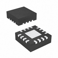
ADS1203 is available in TSSOP-8 and QFN-16 (3x3)
packages.
VDD (AVDD)
VIN+
VIN−
VDD (BVDD)
MDAT
Second−Order
∆Σ Modulator
MCLK
CLKOUT
Buffer
20MHz
RC Oscillator
Interface
Circuit
M0
M1
20kΩ
REFIO
GND (AGND)
2.5V
Reference
Voltage
GND (BGND)
NOTE: BOLD pins are available only in QFN package.
Please be aware that an important notice concerning availability, standard warranty, and use in critical applications of Texas Instruments
semiconductor products and disclaimers thereto appears at the end of this data sheet.
All trademarks are the property of their respective owners.
Copyright 2004−2008, Texas Instruments Incorporated
������!"�# ��!� ��$��
����� �� % ��
�� �� �$ & '��%����� ���
( ���� %��
%��$��
�� �&
%�$�%������ &
� �)
�
�
� �$ !
*�� "����
��� �������� +������,(
���� %���� &��%
����� ��
� ��� �
%
������, ��%� �
�
����� �$ ��� &���
�
��(
www.ti.com
��������
www.ti.com
SBAS318C − JUNE 2004 − REVISED JANUARY 2008
This integrated circuit can be damaged by ESD. Texas Instruments recommends that all integrated circuits be handled with appropriate
precautions. Failure to observe proper handling and installation procedures can cause damage.
ESD damage can range from subtle performance degradation to complete device failure. Precision integrated circuits may be more susceptible to
damage because very small parametric changes could cause the device not to meet its published specifications.
ORDERING INFORMATION
For the most current package and ordering information, see the Package Option Addendum located at the end of
this data sheet, or see the TI website at www.ti.com.
ABSOLUTE MAXIMUM RATINGS(1)
over operating free-air temperature range unless otherwise noted
ADS1203
UNIT
Supply Voltage, AVDD to AGND or VDD to GND
−0.3 to 6
V
Supply Voltage, BVDD to BGND
−0.3 to 6
V
Analog Input Voltage with Respect to AGND or GND
AGND − 0.3 to AVDD + 0.3
V
Reference Input Voltage with Respect to AGND
AGND − 0.3 to AVDD + 0.3
V
Digital Input Voltage with Respect to BGND or GND
BGND − 0.3 to BVDD + 0.3
V
±0.3
V
−0.3 to 6
V
±10
mA
Ground Voltage Difference, AGND to BGND
Voltage Differences, BVDD to AGND
Input Current to Any Pin Except Supply
Power Dissipation
See Dissipation Rating Table
Operating Virtual Junction Temperature Range, TJ
−40 to +150
°C
Operating Free-Air Temperature Range, TA
−40 to +125
°C
Storage Temperature Range, TSTG
−65 to +150
°C
(1) Stresses beyond those listed under Absolute Maximum Ratings may cause permanent damage to the device. These are stress ratings only, and
functional operation of the device at these or any other conditions beyond those indicated under Recommended Operating Conditions is not
implied. Exposure to absolute-maximum-rated conditions for extended periods may affect device reliability.
RECOMMENDED OPERATING CONDITIONS
PARAMETER
MIN
NOM
MAX
UNIT
Supply Voltage, AVDD to AGND or VDD to GND
4.5
5
5.5
V
Supply Voltage, BVDD to BGND
Low-Voltage Levels
2.7
3.6
V
5V Logic Levels
4.5
5
5.5
V
0.5
2.5
2.6
V
Reference Input Voltage
Operating Common-Mode Signal
VIN+ − VIN− (TSSOP package)
Analog Inputs
VIN+ − VIN− (QFN package)
0
5
V
−250
+250
mV
−0.1 × REFIO
External Clock(1)
16
20
Operating Junction Temperature Range, TJ
−40
(1) With reduced accuracy, clock can go from 1MHz up to 32MHz; see Typical Characteristic curves.
+0.1 × REFIO
V
24
MHz
+150
°C
DISSIPATION RATINGS
PACKAGE
TA ≤ +25°C
POWER RATING
DERATING FACTOR
ABOVE TA = +25°C(1)
TA = +70°C
POWER RATING
TA = +85°C
POWER RATING
TA = +1255C
POWER RATING
TSSOP-8
532mW
4.3mW/°C
338mW
274mW
102mW
QFN-16
2540mW
20.4mW/°C
1622mW
1316mW
500mW
(1) This is the inverse of the traditional junction-to-ambient thermal resistance (RqJA). Thermal resistances are not production tested and are for
informational purposes only.
2
��������
www.ti.com
SBAS318C − JUNE 2004 − REVISED JANUARY 2008
ELECTRICAL CHARACTERISTICS
Over recommended operating free-air temperature range at −40°C to +125°C, AVDD = BVDD = +5V or VDD = +5V, VIN+ = −250mV to +250mV,
VIN− = 0V, Mode 3, MCLK input = 20MHz, and 16-bit Sinc3 filter, with OSR = 256, unless otherwise noted.
ADS1203I
PARAMETER
TEST CONDITIONS
Resolution
MIN
TYP(1)
MAX
16
UNITS
Bits
DC Accuracy
INL
Integral linearity error(2)
DNL
Differential nonlinearity(3)
VOS
Input offset(4)
TCVOS
Input offset drift
GERR
Gain error(4)
TCGERR
Gain error drift
PSRR
Power-supply rejection ratio
±1
TA = −40°C to +85°C
±220
REFIO = internal 2.5V
REFIO = internal 2.5V, TA = −40°C to +85°C
4.5V < AVDD or VDD < 5.5V
LSB
±3
LSB
±1
LSB
±1000
±3.5
±8
±0.2
±1.4
−1
TA = −40°C to +85°C
±4
1
µV
µV/°C
%
%
±30
ppm/°C
±20
ppm/°C
80
dB
Analog Input
FSR
Full-scale differential range
Input capacitance
Input leakage current
Differential input resistance
±320
(VIN+) − (VIN−)
Operating common-mode
signal(3)
−0.1
Common-mode
Equivalent
Differential input capacitance
At DC
CMRR
Common-mode rejection ratio
5
V
±16
nA
±1
nA
3
TA = −40°C to +85°C
VIN = 0V to 5V at 50kHz
mV
pF
28
kΩ
5
pF
92
dB
105
dB
Internal Clock for Modes 0, 1, and 2
8.7
Clock frequency
TA = −40°C to +85°C
10
9
11
MHz
11
MHz
24
MHz
External Clock for Mode 3
Clock frequency(5)
16
20
(1) All typical values are at TA = +25°C.
(2) Integral nonlinearity is defined as the maximum deviation of the line through the end points of the specified input range of the transfer curve
for VIN+ = −250mV to +250mV, expressed either as the number of LSBs or as a percent of measured input range (500mV).
(3) Ensured by design.
(4) Maximum values, including temperature drift, are ensured over the full specified temperature range.
(5) With reduced accuracy, the supported external clock frequency range is 1MHz up to 32MHz.
(6) Available only for QFN package.
(7) Applicable for 5.0V nominal supply: BVDD = 4.5V to 5.5V.
(8) Applicable for 3.0V nominal supply: BVDD = 2.7V to 3.6V.
(9) Measured with CLKOUT pin not loaded.
3
��������
www.ti.com
SBAS318C − JUNE 2004 − REVISED JANUARY 2008
ELECTRICAL CHARACTERISTICS (continued)
Over recommended operating free-air temperature range at −40°C to +125°C, AVDD = BVDD = +5V or VDD = +5V, VIN+ = −250mV to +250mV,
VIN− = 0V, Mode 3, MCLK input = 20MHz, and 16-bit Sinc3 filter, with OSR = 256, unless otherwise noted.
ADS1203I
PARAMETER
TEST CONDITIONS
MIN
TYP(1)
81
85
MAX
UNITS
AC Accuracy
SINAD
Signal-to-noise + distortion
SNR
Signal-to-noise ratio
THD
Total harmonic distortion
SFDR
Spurious-free dynamic range
VIN = ±250mVPP at 5kHz
VIN = ±250mVPP at 5kHz, TA = −40°C to +85°C
82.5
VIN = ±250mVPP at 5kHz
81.5
VIN = ±250mVPP at 5kHz, TA = −40°C to +85°C
dB
dB
85
dB
83
VIN = ±250mVPP at 5kHz
dB
−95
VIN = ±250mVPP at 5kHz, TA = −40°C to +85°C
VIN = ±250mVPP at 5kHz
88
VIN = ±250mVPP at 5kHz, TA = −40°C to +85°C
90
−87
dB
−88
dB
95
dB
dB
Voltage Reference Output(6)
VOUT
dVOUT/dT
Reference voltage output
Reference voltage temperature
drift
Output voltage noise
2.440
2.5
2.560
V
±30
ppm/°C
TA = −40°C to +85°C
f = 0.1Hz to 10Hz, CL = 10µF
±20
ppm/°C
10
µVrms
f =10Hz to 10kHz, CL = 10µF
12
µVrms
PSRR
Power-supply rejection ratio
60
dB
IOUT
Output current
10
µA
ISC
Short-circuit current
0.5
mA
100
µs
Turn-on settling time
To 0.1% at CL = 0
Voltage Reference Input(6)
VIN
Reference voltage input
0.5
Reference input resistance
2.5
2.6
20
Reference input capacitance
V
kΩ
5
pF
Reference input current
1
µA
Digital Inputs(7)
Logic family
CMOS with Schmitt Trigger
VIH
High-level input voltage
0.7×BVDD
BVDD+0.3
V
VIL
Low-level input voltage
−0.3
0.3×BVDD
V
IIN
Input current
±50
nA
VIN = BVDD or GND
CI
Input capacitance
Digital Outputs(7)
5
Logic family
CMOS
VOH
High-level output voltage
BVDD = 4.5V, IOH = −100µA
VOL
Low-level output voltage
BVDD = 4.5V, IOL = +100µA
CL
Load capacitance
Data format
pF
4.44
V
0.5
V
30
pF
Bit Stream
(1) All typical values are at TA = +25°C.
(2) Integral nonlinearity is defined as the maximum deviation of the line through the end points of the specified input range of the transfer curve
for VIN+ = −250mV to +250mV, expressed either as the number of LSBs or as a percent of measured input range (500mV).
(3) Ensured by design.
(4) Maximum values, including temperature drift, are ensured over the full specified temperature range.
(5) With reduced accuracy, the supported external clock frequency range is 1MHz up to 32MHz.
(6) Available only for QFN package.
(7) Applicable for 5.0V nominal supply: BVDD = 4.5V to 5.5V.
(8) Applicable for 3.0V nominal supply: BVDD = 2.7V to 3.6V.
(9) Measured with CLKOUT pin not loaded.
4
��������
www.ti.com
SBAS318C − JUNE 2004 − REVISED JANUARY 2008
ELECTRICAL CHARACTERISTICS (continued)
Over recommended operating free-air temperature range at −40°C to +125°C, AVDD = BVDD = +5V or VDD = +5V, VIN+ = −250mV to +250mV,
VIN− = 0V, Mode 3, MCLK input = 20MHz, and 16-bit Sinc3 filter, with OSR = 256, unless otherwise noted.
ADS1203I
TEST CONDITIONS
PARAMETER
Digital Inputs(6)(8)
MIN
Logic family
TYP(1)
MAX
UNITS
LVCMOS
VIH
High-level input Voltage
BVDD = 3.6V
2
BVDD+0.3
VIL
Low-level input voltage
BVDD = 2.7V
−0.3
0.8
V
IIN
Input current
VI = BVDD or GND
±50
nA
CI
Input capacitance
5
V
pF
Digital Outputs(6)(8)
Logic family
LVCMOS
VOH
VOL
High-level output voltage
BVDD = 2.7V, IOH = −100µA
Low-level output voltage
BVDD = 2.7V, IOL = +100µA
CL
Load capacitance
BVDD−0.2
V
0.2
V
30
pF
4.5
5.5
V
Data format
Bit Stream
Power Supply
VDD
AVDD(6)
BVDD(6)
IDD
AIDD(6)
BIDD(6)
Supply voltage
Analog supply voltage
Buffer I/O supply voltage
Supply current
Analog operating supply current
Buffer I/O operating supply
current
4.5
5.5
V
Low-voltage levels
2.7
3.6
V
5V logic levels
4.5
5.5
V
Mode 0
8.4
10.5
mA
Mode 3
6.7
8.5
mA
Mode 0
6.2
7.5
mA
Mode 3
5.9
6.9
mA
BVDD = 3V, Mode 0
2.2
2.3
mA
BVDD = 3V, Mode 3(9)
0.8
0.9
mA
42
49
mW
33.5
39
mW
Mode 0
Power dissipation
Mode 3(9)
(1) All typical values are at TA = +25°C.
(2) Integral nonlinearity is defined as the maximum deviation of the line through the end points of the specified input range of the transfer curve
for VIN+ = −250mV to +250mV, expressed either as the number of LSBs or as a percent of measured input range (500mV).
(3) Ensured by design.
(4) Maximum values, including temperature drift, are ensured over the full specified temperature range.
(5) With reduced accuracy, the supported external clock frequency range is 1MHz up to 32MHz.
(6) Available only for QFN package.
(7) Applicable for 5.0V nominal supply: BVDD = 4.5V to 5.5V.
(8) Applicable for 3.0V nominal supply: BVDD = 2.7V to 3.6V.
(9) Measured with CLKOUT pin not loaded.
EQUIVALENT INPUT CIRCUIT
VDD
(AVDD)
VDD
(BVDD)
RON = 350Ω C(SAMPLE) = 5pF
AIN
DIN
GND
(AGND)
Diode Turn on Voltage: 0.4V
Equivalent Analog Input Circuit
GND
(BGND)
Equivalent Digital Input Circuit
5
��������
www.ti.com
SBAS318C − JUNE 2004 − REVISED JANUARY 2008
PIN ASSIGNMENTS: PW (TSSOP) PACKAGE
PIN ASSIGNMENTS: RGT (QFN) PACKAGE
2
VIN−
3
6
MDAT
M1
4
5
GND
VIN−
3
NC
4
M0
NC
NC
AVDD
15
14
13
ADS1203
12
BVDD
11
MCLK
10
CLKOUT
9
8
VIN+
MCLK
ADS1203
BGND
1
7
REFIO
AGND
7
6
VIN+
2
VDD
NC
8
5
1
M1
M0
16
RGT PACKAGE(1)
QFN-16
(TOP VIEW)
PW PACKAGE
TSSOP-8
(TOP VIEW)
MDAT
(1) The thermal pad is internally connected to the substrate. This pad
can be connected to the analog ground or left floating. Keep the
thermal pad separate from the digital ground, if possible.
Terminal Functions: PW (TSSOP) Package
Terminal Functions: RGT (QFN) Package
TERMINAL
NAME
TERMINAL
NO.
I/O
M0
1
I
VIN+
2
VIN−
3
M1
4
GND
5
MDAT
6
O
MCLK
7
I/O
VDD
8
DESCRIPTION
NAME
NO.
I/O
Mode input
REFIO
1
I/O
I
Noninverting analog input
VIN+
2
I
Noninverting analog input
I
Inverting analog input
VIN−
3
I
Inverting analog input
I
Mode input
NC
4, 6, 14, 15
I
Not connected
Power supply ground
M1
5
I
Mode input
Modulator data output
AGND
7
Analog power-supply ground
Modulator clock input or output
BGND
8
Interface power-supply ground
Power supply: +5V nominal
MDAT
9
O
Modulator data output
CLKOUT
10
O
Modulator clock output (Mode 3 only)
MCLK
11
I/O
Modulator clock input or output
BVDD
12
Interface power supply
AVDD
13
Analog power supply
M0
16
Mode input
NOTE: For the TSSOP package, BGND and AGND are internally
connected to the GND pin. Additionally, the AVDD and BVDD
pins are connected to VDD.
6
DESCRIPTION
Reference voltage input/output
��������
www.ti.com
SBAS318C − JUNE 2004 − REVISED JANUARY 2008
PARAMETER MEASUREMENT INFORMATION
tC1
MCLK
tW1
tD1
MDAT
Figure 1. Mode 0 Operation
TIMING CHARACTERISTICS: MODE 0
Over recommended operating free-air temperature range at −40°C to +125°C, AVDD = BVDD = +5V(1) or AVDD = +5V, BVDD = +3V(2) or VDD = +5V(1),
unless otherwise noted.
PARAMETER
MODE
MIN
MAX
UNIT
tC1
Clock period
0
91
111
ns
tW1
Clock high time
0
(tC1/2) − 5
(tC1/2) + 5
ns
tD1
Data delay after falling edge of clock
0
−2
2
ns
(1) Applicable for 5.0V nominal supply: BVDD (min) = 4.5V and BVDD (max) = 5.5V.
(2) Only for QFN package. Applicable for 3.0V nominal supply: BVDD (min) = 2.7V and BVDD (max) = 3.6V.
t C2
MCLK
tD2
t W2
tD3
MDAT
Figure 2. Mode 1 Operation
TIMING CHARACTERISTICS: MODE 1
Over recommended operating free-air temperature range at −40°C to +125°C, AVDD = BVDD = +5V(1) or AVDD = +5V, BVDD = +3V(2) or VDD = +5V(1),
unless otherwise noted.
PARAMETER
MODE
MIN
MAX
UNIT
tC2
Clock period
1
182
222
ns
tW2
Clock high time
1
(tC2/2) − 5
(tC2/2) + 5
ns
tD2
Data delay after rising edge of clock
1
(tW2/2) − 2
(tW2/2) + 2
ns
tD3
Data delay after falling edge of clock
1
(tW2/2) − 2
(tW2/2) + 2
ns
(1) Applicable for 5.0V nominal supply: BVDD (min) = 4.5V and BVDD (max) = 5.5V.
(2) Only for QFN package. Applicable for 3.0V nominal supply: BVDD (min) = 2.7V and BVDD (max) = 3.6V.
7
��������
www.ti.com
SBAS318C − JUNE 2004 − REVISED JANUARY 2008
tC 1
Internal
MCLK
tW 1
Internal
MDATA
1
0
1
1
0
0
MDATA
Figure 3. Mode 2 Operation
TIMING CHARACTERISTICS: MODE 2
Over recommended operating free-air temperature range at −40°C to +125°C, AVDD = BVDD = +5V(1) or AVDD = +5V, BVDD = +3V(2) or VDD = +5V(1),
unless otherwise noted.
PARAMETER
MIN
MAX
tC1
Clock period
MODE
2
91
111
UNIT
ns
tW1
Clock high time
2
(tC1/2) − 5
(tC1/2) + 5
ns
(1) Applicable for 5.0V nominal supply: BVDD (min) = 4.5V and BVDD (max) = 5.5V.
(2) Only for QFN package. Applicable for 3.0V nominal supply: BVDD (min) = 2.7V and BVDD (max) = 3.6V.
tC1
MCLK
tC2
tW1
tD1
tD2
CLKOUT(1)
t W2
tD3
tD4
MDAT
NOTE: (1) CLKOUT availble only on QFN package.
Figure 4. Mode 3 Operation
TIMING CHARACTERISTICS: MODE 3
Over recommended operating free-air temperature range at −40°C to +125°C, AVDD = BVDD = +5V(1) or AVDD = +5V, BVDD = +3V(2) or VDD = +5V(1),
unless otherwise noted.
PARAMETER
MIN
MAX
UNIT
tC1
MCLK period
41.6
1000
ns
tW1
MCLK high time
10
tC1 − 10
ns
tC2
CLKOUT period
2 × tC1
2 × tC1
ns
tW2
CLKOUT high time
(tC2/2) − 5
(tC2/2) + 5
ns
tD1
CLKOUT rising edge delay after MCLK rising edge
0
10
ns
tD2
CLKOUT falling edge delay after MCLK rising edge
0
10
ns
tD3
Data valid delay after rising edge of CLKOUT
−2
+2
ns
tD4
Data valid delay after rising edge of MCLK
0
10
ns
:
NOTE Input signal is specified with tR = tF = 5ns (10% to 90% of BVDD or VDD) and timed from a voltage level of (VIL + VIH)/2. See timing diagram.
(1) Applicable for 5.0V nominal supply: BVDD (min) = 4.5V and BVDD (max) = 5.5V.
(2) Only for QFN package. Applicable for 3.0V nominal supply: BVDD (min) = 2.7V and BVDD (max) = 3.6V.
8
��������
www.ti.com
SBAS318C − JUNE 2004 − REVISED JANUARY 2008
TYPICAL CHARACTERISTICS
AVDD = BVDD = +5V or VDD = +5V, VIN+ = −250mV to +250mV, VIN− = 0V, MCLK input = 20MHz, and 16-bit Sinc3 filter, with OSR = 256, unless
otherwise noted.
INTEGRAL NONLINEARITY vs INPUT SIGNAL
(Mode 3, MCLK = 20MHz)
4
4
3
3
2
2
1
1
0
INL (LSB)
INL (LSB)
INTEGRAL NONLINEARITY vs INPUT SIGNAL
(Mode 0)
−40_C
−1
+85_C
−2
+25_C
−1
+85_C
−2
+25_C
−3
−40_ C
0
−3
−4
−4
−5
−320
−240
−160
−80
0
80
160
240
−5
−320
320
−240
Differential Input Voltage (mV)
−160
−80
0
80
160
240
320
Differential Input Voltage (mV)
INTEGRAL NONLINEARITY vs INPUT SIGNAL
(Mode 3, MCLK = 32MHz)
INTEGRAL NONLINEARITY vs TEMPERATURE
5
4
0.0076
3
Mode 3 (MCLK = 32MHz)
4
0.0061
INL (LSB)
INL (LSB)
1
0
+85_C
−1
−40_C
−2
3
0.0046
Mode 0
2
0.0031
Mode 3 (MCLK = 20MHz)
−3
1
0.0015
+25_C
−4
−5
−320
0
−240
−160
−80
0
80
160
240
320
−40
−20
0
OFFSET vs TEMPERATURE
40
60
80
0
100
OFFSET vs POWER SUPPLY
0
0
Mode 0
−100
−100
Mode 3 (MCLK = 20MHz)
−200
−200
−300
Offset (µV)
Offset (µV)
20
Temperature (_C)
Differential Input Voltage (mV)
Mode 3 (MCLK = 20MHz)
−400
−500
−300
Mode 0
−400
−500
Mode 3 (MCLK = 32MHz)
−600
−600
−700
INL (%)
2
Mode 3 (MCLK = 32MHz)
−800
−40
−20
−700
−800
0
20
40
Temperature (_C)
60
80
100
4.5
4.6
4.7
4.8
4.9
5
5.1
5.2
5.3
5.4
5.5
Power Supply (V)
9
��������
www.ti.com
SBAS318C − JUNE 2004 − REVISED JANUARY 2008
TYPICAL CHARACTERISTICS (continued)
AVDD = BVDD = +5V or VDD = +5V, VIN+ = −250mV to +250mV, VIN− = 0V, MCLK input = 20MHz, and 16-bit Sinc3 filter, with OSR = 256, unless
otherwise noted.
GAIN vs TEMPERATURE
RMS NOISE vs INPUT VOLTAGE LEVEL
14
0.10
Mode 0
0
12
RMS Noise (µV)
Gain (%)
−0.10
Mode 3 (MCLK = 20MHz)
−0.20
−0.30
8
6
4
Mode 3 (MCLK = 32MHz)
−0.40
−0.50
−40
10
2
−20
0
20
40
Temperature (_ C)
60
80
0
−320
100
−240
−80
0
80
160
240
320
Differential Input Voltage (mV)
SIGNAL−TO−NOISE + DISTORTION
vs TEMPERATURE
SIGNAL−TO−NOISE RATIO vs TEMPERATURE
85.6
85.2
Mode 3 (MCLK = 32MHz)
Mode 3 (MCLK = 20MHz)
84.8
85.4
84.4
84.0
85.2
Mode 3 (MCLK = 20MHz)
85.0
SINAD (dB)
SNR (dB)
−160
84.8
84.6
83.6
83.2
Mode 0
82.8
82.4
82.0
Mode 0
Mode 3 (MCLK = 32MHz)
81.6
84.4
81.2
84.2
−40
−20
0
20
40
60
80
80.8
100
−40
−20
0
Temperature (_C)
EFFECTIVE NUMBER OF BITS
vs DECIMATION RATIO
20
40
Temperature (_ C)
60
80
100
POWER−SUPPLY CURRENT vs TEMPERATURE
18
110
16
98
14
86
10
74
Sinc2
Filter
10
62
8
50
6
38
Current (mA)
Sinc3 Filter
12
SNR (dB)
ENOB (Bits)
Mode 3 (MCLK = 32MHz)
9
Mode 0
8
Mode 3 (MCLK = 20MHz)
7
6
26
4
10
100
1k
Decimation Ratio (OSR)
10
10k
5
−40
−20
0
20
40
Temperature (_ C)
60
80
100
��������
www.ti.com
SBAS318C − JUNE 2004 − REVISED JANUARY 2008
TYPICAL CHARACTERISTICS (continued)
AVDD = BVDD = +5V or VDD = +5V, VIN+ = −250mV to +250mV, VIN− = 0V, MCLK input = 20MHz, and 16-bit Sinc3 filter, with OSR = 256, unless
otherwise noted.
SPURIOUS−FREE DYNAMIC RANGE AND
TOTAL HARMONIC DISTORTION vs TEMPERATURE
(Mode 0)
SPURIOUS−FREE DYNAMIC RANGE AND
TOTAL HARMONIC DISTORTION vs TEMPERATURE
(Mode 3, MCLK = 20MHz)
105
0.5VPP
5kHz
105
−105
−101
99
−99
99
−99
97
−97
95
−95
SFDR
−93
93
−91
91
−89
89
87
−87
87
85
−85
85
91
THD
89
−40
−20
0
20
40
Temperature (_C)
60
80
−105
SFDR
−89
60
80
100
−110
−97
95
−95
93
−93
91
−91
SFDR (dB)
97
90
THD (dB)
SFDR (dB)
20
40
Temperature (_ C)
100
−99
THD
−89
89
0.5VPP
5kHz
SFDR
−100
THD
−90
80
−80
70
−70
60
−60
−87
−85
85
−20
−85
0
110
−101
−40
−20
−87
−103
101
87
−91
SPURIOUS−FREE DYNAMIC RANGE AND
TOTAL HARMONIC DISTORTION vs INPUT FREQUENCY
(Mode 0)
105
99
−93
0.5VPP
5kHz
SPURIOUS−FREE DYNAMIC RANGE
AND TOTAL HARMONIC DISTORTION
vs TEMPERATURE (Mode 3, MCLK = 32MHz)
103
−95
THD
−40
100
−97
SFDR
95
THD (dB)
93
97
THD (dB)
−103
101
SFDR (dB)
103
−101
THD (dB)
−103
101
103
SFDR (dB)
−105
0
20
40
Temperature (_ C)
60
80
−50
50
100
1
10
20
Frequency (kHz)
SPURIOUS−FREE DYNAMIC RANGE AND
TOTAL HARMONIC DISTORTION vs INPUT FREQUENCY
(Mode 3, MCLK = 20MHz)
SPURIOUS−FREE DYNAMIC RANGE AND
TOTAL HARMONIC DISTORTION vs INPUT FREQUENCY
(Mode 3, MCLK = 32MHz)
−110
110
−110
110
SFDR
−100
THD
SFDR (dB)
90
−90
80
−80
70
−70
−60
60
−60
−50
50
80
−80
70
−70
OSR = 256
Sinc3 Filter
50
1
10
Frequency (kHz)
20
SFDR (dB)
−90
SFDR
THD (dB)
THD
90
60
−100
100
THD (dB)
100
−50
1
10
20
Frequency (kHz)
11
��������
www.ti.com
SBAS318C − JUNE 2004 − REVISED JANUARY 2008
TYPICAL CHARACTERISTICS (continued)
AVDD = BVDD = +5V or VDD = +5V, VIN+ = −250mV to +250mV, VIN− = 0V, MCLK input = 20MHz, and 16-bit Sinc3 filter, with OSR = 256, unless
otherwise noted.
FREQUENCY SPECTRUM
(4096 Point FFT, fIN = 5kHz, 0.5VPP)
0
0
−20
−20
−40
−40
Magnitude (dB)
Magnitude (dB)
FREQUENCY SPECTRUM
(4096 Point FFT, fIN = 1kHz, 0.5VPP)
−60
−80
−100
−60
−80
−100
−120
−120
−140
−140
0
5
10
15
20
0
5
Frequency (kHz)
CLOCK FREQUENCY vs TEMPERATURE
15
20
CLOCK FREQUENCY vs POWER SUPPLY
10.8
10.5
10.5
10.3
MCLK (MHz)
MCLK (MHz)
10
Frequency (kHz)
10.2
9.9
9.6
10.1
9.9
9.7
9.3
9.5
−40
−20
0
20
40
Temperature (_ C)
60
80
100
4.5
COMMON−MODE REJECTION RATIO
vs FREQUENCY
4.7
4.9
5.1
Power Supply (V)
5.3
5.5
POWER−SUPPLY REJECTION RATIO
vs FREQUENCY
110
90
105
85
100
80
PSRR (dB)
CMRR (dB)
95
90
85
80
75
75
70
65
60
70
55
65
50
60
1
12
10
Input Frequency (kHz)
100
0.1
1
10
Frequency of Power Supply (kHz)
100
��������
www.ti.com
SBAS318C − JUNE 2004 − REVISED JANUARY 2008
TYPICAL CHARACTERISTICS (continued)
AVDD = BVDD = +5V or VDD = +5V, VIN+ = −250mV to +250mV, VIN− = 0V, MCLK input = 20MHz, and 16-bit Sinc3 filter, with OSR = 256, unless
otherwise noted.
MCLK AND MDAT
TYPICAL SINK CURRENT
MCLK AND MDAT
TYPICAL SOURCE CURRENT
70
80
5.5V
70
Output Current, IOH (mA)
50
5V
40
4.5V
30
20
10
60
5.5V
50
5V
40
30
4.5V
20
10
0
0
0
1
2
3
4
5
6
0
1
Output Voltage, VOL (V)
2
3
4
Output Voltage, VOH (V)
5
6
REFERENCE VOLTAGE vs TEMPERATURE
2.503
2.502
2.501
VREF (V)
Output Current, IOL (mA)
60
2.500
2.499
2.498
2.497
−40
−20
0
20
40
60
80
100
Temperature (_C)
13
��������
www.ti.com
SBAS318C − JUNE 2004 − REVISED JANUARY 2008
GENERAL DESCRIPTION
The ADS1203 is a single-channel, 2nd-order, CMOS
delta-sigma modulator, designed for medium- to
high-resolution A/D conversions from DC to 39kHz with
an oversampling ratio (OSR) of 256. The output of the
converter (MDAT) provides a stream of digital ones and
zeros. The time average of this serial output is
proportional to the analog input voltage.
The modulator shifts the quantization noise to high
frequencies. A low-pass digital filter should be used at
the output of the delta-sigma modulator. The primary
purpose of the digital filter is to filter out high-frequency
noise. The secondary purpose is to convert the 1-bit
data stream at a high sampling rate into a higher-bit
data word at a lower rate (decimation). A digital signal
processor (DSP), microcontroller (µC), or field
programmable gate array (FPGA) could be used to
implement the digital filter. Figure 6 shows the
ADS1203 connected to a DSP.
The overall performance (speed and accuracy)
depends on the selection of an appropriate OSR and
filter type. A higher OSR produces greater output
accuracy while operating at a lower refresh rate.
Alternatively, a lower OSR produces lower output
accuracy, but operates at a higher refresh rate. This
system allows flexibility with the digital filter design and
is capable of A/D conversion results that have a
dynamic range exceeding 95dB with an OSR = 256.
this can only be used in mode 3). The analog input
signal is continuously sampled by the modulator and
compared to an internal voltage reference. A digital
stream, which accurately represents the analog input
voltage over time, appears at the output of the
converter.
REFERENCE
Under normal operation, REFIO (pin 1) provides an
internal +2.5V reference to the ADS1203. However, the
ADS1203 can operate with an external reference in the
range of 0.5V to 2.6V, for a corresponding full-scale
range of 0.256 × REFIO, as long as the input does not
exceed the AVDD + 0.3V value. The recommended input
range is ±0.1 × REFIO.
The ADS1203 reference is double-buffered. If the
internal reference is used to drive an external load, it
can only drive a high-impedance load because
RI = 20kΩ. If an external reference voltage is used, the
external source must be capable of driving the 20kΩ
resistor. To minimize noise, a 0.1µF capacitor should be
connected to REFIO.
Reference
Voltage
Buffer
20kΩ
THEORY OF OPERATION
The differential analog input of the ADS1203 is
implemented with a switched-capacitor circuit. This
circuit implements a 2nd-order modulator stage, which
digitizes the analog input signal into a 1-bit output
stream. The clock source can be internal as well as
external. Different frequencies for this clock allow for a
variety of solutions and signal bandwidths (however,
REFIO
Figure 5. REFIO Voltage Reference Connection
+3V
+5V
DSP
ADS1203
M
VDDO
AVDD
10nF
27Ω
27Ω
1nF
1nF
0.1µF
M0
BVDD
VIN+
MCLK
SPICLK
VIN−
MDAT
SPISIMO
M1
BGND
VSSO
AGND
Figure 6. Connection Diagram for the ADS1203 Delta-Sigma Modulator Including DSP
14
��������
www.ti.com
SBAS318C − JUNE 2004 − REVISED JANUARY 2008
ANALOG INPUT STAGE
Z IN +
Analog Input
The input design topology of the ADS1203 is based on
a fully differential switched-capacitor architecture. This
input stage provides the mechanism to achieve low
system noise, high common-mode rejection (92dB),
and excellent power-supply rejection.
The input impedance of the analog input depends on
the modulator clock frequency (fCLK), which is also the
sampling frequency of the modulator. Figure 7 shows
the basic input structure of the ADS1203. The
relationship between the input impedance of the
ADS1203 and the modulator clock frequency is:
28kW
f CLKń10MHz
The input impedance becomes a consideration in
designs where the source impedance of the input signal
is high. This may cause a degradation in gain, linearity
and THD. The importance of this effect depends on the
desired system performance. There are two restrictions
on the analog input signals, VIN+ and VIN−. If the input
voltage exceeds the range GND – 0.4V to VDD + 0.3V,
the input current must be limited to 10mA because the
input protection diodes on the front end of the converter
will begin to turn on. In addition, the linearity and the
noise performance of the device are ensured only when
the differential analog voltage resides within ±250mV;
however, the FSR input voltage is ±320mV.
RSW
350Ω(typ)
High
Impedance
> 1GΩ
AIN+
CINT
7pF (typ)
1.5pF
Switching Frequency
= CLK
VCM
1.5pF
RSW
350Ω(typ)
AIN−
(1)
CINT
7pF (typ)
High
Impedance
> 1GΩ
Figure 7. Input Impedance of the ADS1203
15
��������
www.ti.com
SBAS318C − JUNE 2004 − REVISED JANUARY 2008
Modulator
The ADS1203 can be operated in four modes. Modes
0, 1, and 2 use the internal clock, which is fixed at
20MHz. The modulator can also be operated with an
external clock in mode 3. In all modes, the clock is
divided by 2 internally and is used as the modulator
clock. The frequency of the external clock can vary from
1MHz to 32MHz to adjust for the clock requirements of
the application.
The modulator topology is fundamentally a 2nd-order,
switched-capacitor, delta-sigma modulator, such as the
one conceptualized in Figure 8. The analog input
voltage and the output of the 1-bit digital-to-analog
converter (DAC) are differentiated, providing analog
voltages at X2 and X3. The voltages at X2 and X3 are
presented to the respective individual integrators. The
output of these integrators progresses in a negative or
positive direction. When the value of the signal at X4
equals the comparator reference voltage, the output of
the comparator switches from negative to positive, or
positive to negative, depending on its original state.
When the output value of the comparator switches from
high to low or vice versa, the 1-bit DAC responds on the
next clock pulse by changing its analog output voltage
at X6, causing the integrators to progress in the
opposite direction. The feedback of the modulator to the
front end of the integrators forces the value of the
integrator output to track the average of the input.
fCLK
X(t)
X2
Integrator 1
X3
Integrator 2
X4
DATA
fS
VREF
Comparator
X6
D/A Converter
Figure 8. Block Diagram of the 2nd-Order Modulator
16
��������
www.ti.com
SBAS318C − JUNE 2004 − REVISED JANUARY 2008
DIGITAL OUTPUT
A differential input signal of 0V ideally produces a
stream of ones and zeros that is high 50% of the time
and low 50% of the time. A differential input of +256mV
produces a stream of ones and zeros that is high 80%
of the time. A differential input of –256mV produces a
stream of ones and zeros that is high 20% of the time.
The input voltage versus the output modulator signal is
shown in Figure 9.
DIGITAL INTERFACE
INTRODUCTION
The analog signal that is connected to the input of the
delta-sigma modulator is converted using the clock
signal applied to the modulator. The result of the
conversion, or modulation, is the output signal DATA
from the delta-sigma modulator. In most applications
where a direct connection is realized between the
delta-sigma modulator and an ASIC, FPGA, DSP, or µC
(each with an implemented filter), the two standard
signals (MCLK and MDAT) are provided from the
modulator. To reduce the wiring (for example, for
galvanic isolation), a single line is preferred. Therefore,
in mode 2, the data stream is Manchester-encoded.
MODES OF OPERATION
The system clock of the ADS1203 is 20MHz by default.
The system clock can be provided either from the
internal 20MHz RC oscillator or from an external clock
source. For this purpose, the MCLK pin is bidirectional
and controlled by the mode setting.
The system clock is divided by 2 for the modulator
clock. Therefore, the default clock frequency of the
modulator is 10MHz. With a possible external clock
range of 1MHz to 32MHz, the modulator operates
between 500kHz and 16MHz.
The four modes of operation for the digital data interface
are shown in Table 1.
Modulator Output
+FS (Analog Input)
−FS (Analog Input)
Analog Input
Figure 9. Analog Input vs Modulator Output of the ADS1203
Table 1. Digital Data Interface Modes of Operation
MODE
DEFINITION
M1
M0
0
Internal clock, synchronous data output
Low
Low
1
Internal clock, synchronous data output, half output clock frequency
Low
High
2
Internal clock, Manchester-encoded data output
High
Low
3
External clock, synchronous data output
High
High
17
��������
www.ti.com
SBAS318C − JUNE 2004 − REVISED JANUARY 2008
Mode 0
In mode 0, the internal RC oscillator is running. The data
are provided at the MDAT output pin, and the modulator
clock at the MCLK pin. The data change at the falling
edge of MCLK; therefore, the data can safely be
strobed with the rising edge. See Figure 1 on page 7.
Mode 1
In mode 1, the internal RC oscillator is running. The data
are provided at the MDAT output pin. The MCLK pin
provides the half modulator clock. The data must be
strobed at both the rising and falling edges of MCLK.
The data at MDAT change in the middle, between the
rising and falling edge. In this mode the frequency of
both MCLK and MDAT is only 5MHz. See Figure 2 on
page 7.
Mode 2
This filter provides the best output performance at the
lowest hardware size (for example, count of digital
gates). For oversampling ratios in the range of 16 to
256, this is a good choice. All the characterizations in
the data sheet are also done using a sinc3 filter with an
oversampling ratio of OSR = 256 and an output word
width of 16 bits.
In a sinc3 filter response (shown in Figure 10 and
Figure 11), the location of the first notch occurs at the
frequency of output data rate fDATA = fCLK/OSR. The
–3dB point is located at half the Nyquist frequency or
fDATA/4. For some applications, it may be necessary to
use another filter type for better frequency response.
This performance can be improved, for example, by a
cascaded filter structure. The first decimation stage can
be a sinc3 filter with a low OSR and the second stage
a high-order filter.
In mode 2, the internal RC oscillator is running. The data
are Manchester-encoded and are provided at the
MDAT pin. The MCLK output is set to low. There is no
clock output provided in this mode. The Manchester
coding allows the data transfer with only a single line.
See Figure 3 on page 8.
FILTER USAGE
The modulator generates only a bitstream, which does
not output a digital word like an analog-to-digital
converter (ADC). In order to output a digital word
equivalent to the analog input voltage, the bitstream
must be processed by a digital filter.
A very simple filter built with minimal effort and
hardware is the sinc3 filter:
ǒ
Ǔ
−OSR
H(z) + 1 * z −1
1*z
18
3
(2)
−20
Gain (dB)
In mode 3, the internal RC oscillator is disabled. The
system clock must be provided externally at the input
MCLK. The system clock must have twice the
frequency of the chosen modulator clock. The data are
provided at the MDAT output pin. Because the
modulator runs with the half system clock, the data
change at every other falling edge of the external clock.
The data can safely be strobed at every other rising
edge of MCLK. This mode allows synchronous
operation to any digital system or the use of clocks
different from 10MHz. See Figure 4 on page 8. On the
QFN package, the modulator clock is provided as the
CLKOUT signal. Output data can be strobed at each
rising edge of CLKOUT.
OSR = 32
f DATA = 10MHz/32 = 312.5kHz
−3dB: 81.9kHz
−10
−30
−40
−50
−60
−70
−80
0
200
400
600
800 1000
Frequency (kHz)
1200
1400
1600
Figure 10. Frequency Response of Sinc3 Filter
30k
OSR = 32
FSR = 32768
ENOB = 9.9 Bits
Settling Time =
3 × 1/f DATA = 9.6µs
25k
Output Code
Mode 3
0
20k
15k
10k
5k
0
0
5
10
15
20
25
30
Number of Output Clocks
35
Figure 11. Pulse Response of Sinc3 Filter
(fMOD = 10MHz)
40
��������
www.ti.com
SBAS318C − JUNE 2004 − REVISED JANUARY 2008
The effective number of bits (ENOB) can be used to
compare the performance of ADCs and delta-sigma
modulators. Figure 12 shows the ENOB of the
ADS1203 with different filter types. In this data sheet,
the ENOB is calculated from the SNR:
SNR = 1.76dB + 6.02dB × ENOB
(3)
clocks. The data clock is equal to the modulator clock
divided by the OSR. For overcurrent protection, filter
types other than sinc3 might be a better choice. A simple
example is a sinc2 filter. Figure 13 compares the settling
time of different filter types. The sincfast is a modified
sinc2 filter:
ǒ
Ǔ
2
−OSR
H(z) + 1 * z −1 ǒ1 ) z −2
1*z
16
sinc3
10
14
(4)
sinc3
9
sincfast
12
8
sinc2
8
6
sinc
4
sincfast
7
10
ENOB (Bits)
ENOB (Bits)
Ǔ
OSR
sinc2
6
5
4
sinc
3
2
2
1
0
1
10
100
1000
OSR
Figure 12. Measured ENOB vs OSR
In motor control applications, a very fast response time
for overcurrent detection is required. There is a
constraint between 1µs and 5µs with 3 bits to 7 bits
resolution. The time for full settling depends on the filter
order. Therefore, the full settling of the sinc3 filter needs
three data clocks and the sinc2 filter needs two data
0
0
1
2
3
4
5
6
Settling Time (µs)
7
8
9
10
Figure 13. Measured ENOB vs Settling Time
For more information, see application note SBAA094,
Combining the ADS1202 with an FPGA Digital Filter for
Current Measurement in Motor Control Applications,
available for download at www.ti.com.
19
��������
www.ti.com
SBAS318C − JUNE 2004 − REVISED JANUARY 2008
The DSP (such as a C28x or C24x) can be directly
connected at the output of two channels of the
optocoupler. In this configuration, the signals arriving at
C28x or C24x are standard delta-sigma modulator
signals and are connected directly to the SPICLK and
SPISIMO pins. Being a delta-sigma converter, there is
no need to have word sync on the serial data, so an SPI
is ideal for connection. McBSP would work as well in
SPI mode.
APPLICATIONS
Operating the ADS1203 in a typical application using
mode 0 is shown in Figure 14. Measurement of the
motor phase current is done through the shunt resistor.
For better performance, both signals are filtered. R2 and
C2 filter noise on the noninverting input signal, R3 and C3
filter noise on the inverting input signal, and C4 in
combination with R2 and R3 filter the differential input
signal. In this configuration, the shunt resistor is
connected via three wires with the ADS1203.
When component reduction is necessary, the ADS1203
can operate in mode 2, as shown in Figure 15. M1 is
high and M0 is low. Only the noninverting input signal
is filtered. R2 and C2 filter noise on the input signal. The
inverting input is directly connected to the GND pin,
which is simultaneously connected to the shunt resistor.
The power supply is taken from the upper gate driver
power supply. A decoupling capacitor of 0.1µF is
recommended for filtering the power supply. If better
filtering is required, an additional 1µF to 10µF capacitor
can be added.
The output signal from the ADS1203 is
Manchester-encoded. In this case, only one signal is
transmitted. For that reason, one optocoupler channel
is used instead of two channels, as in the previous
example of Figure 14. Another advantage of this
configuration is that the DSP will use only one line per
channel instead of two. That permits the use of smaller
DSP packages in the application.
The control lines M0 and M1 are both low while the part
is operating in mode 0. Two output signals, MCLK and
MDAT, are connected directly to the optocoupler. The
optocoupler can be connected to transfer a direct or
inverse signal because the output stage has the
capacity to source and sink the same current. The
discharge resistor is not needed in parallel with
optocoupler diodes because the output driver has
push-pull capability to keep the LED diode out of the
charge.
HV+
Floating
Power Supply
Gate
Drive
Circuit
R2
27Ω
RSENSE
R3
27Ω
R1
D1
5.1V
C1
0.1µF
ADS1203
C4
10nF
C2
1nF
C3
1nF
M0
VDD
VIN+
MCLK
VIN−
MDAT
M1
R4
Optocoupler
C28x
or
C24x
SPICLK
SPISIMO
GND
Power Supply
Gate
Drive
Circuit
HV−
Figure 14. Application Diagram in Mode 0
20
R5
��������
www.ti.com
SBAS318C − JUNE 2004 − REVISED JANUARY 2008
HV+
Floating
Power Supply
Gate
Drive
Circuit
R1
D1
5.1V
R2
27Ω
RSENSE
C1
0.1µF
ADS1203
M0
C2
0.1µF
Power
Supply
VIN+
MCLK
VIN−
MDAT
M1
R4
Optocoupler
VDD
C28x
or
C24x
GND
Gate
Drive
Circuit
HV−
Figure 15. Application Diagram in Mode 2
Floating
Power Supply
HV+
C28x
or
C24x
Gate Drive
Circuit
CVDD
ADS1203
R2
27Ω
M0
+
RSENSE
−
C2
0.1µF
C1
0.1µF
VDD
VIN+
MCLK
SPICLK
VIN−
MDAT
SPISIMO
M1
GND
DVDD
Figure 16. Application Diagram without Galvanic Isolation in Mode 0
21
��������
www.ti.com
SBAS318C − JUNE 2004 − REVISED JANUARY 2008
ADS1203
+5V
AVDD
R1
27Ω
+
RSENSE
M0
C1
0.1µF
C4
0.1µF
BVDD
REFIO
VIN+
MCLK
VIN−
MDAT
M1
BGND
AGND
−
ADS1203
+5V
AVDD
R2
27Ω
+
RSENSE
−
C2
0.1µF
C5
0.1µF
BVDD
REFIO
M0
VIN+
MCLK
VIN−
MDAT
M1
BGND
AGND
C28x
or
C24x
+3V
CVDD
ADS1203
+5V
AVDD
R3
27Ω
+
RSENSE
−
C3
0.1µF
C6
0.1µF
SPICLK
BVDD
SPISIMO
M0
REFIO
SPISIMO
VIN+
MCLK
VIN−
MDAT
M1
BGND
AGND
SPISIMO
CLK
DVDD
Figure 17. Application Diagram without Galvanic Isolation in Mode 3
22
��������
www.ti.com
SBAS318C − JUNE 2004 − REVISED JANUARY 2008
LAYOUT CONSIDERATIONS
Power Supplies
The ADS1203 requires only one power supply (VDD). If
there are separate analog and digital power supplies on
the board, a good design approach is to have the
ADS1203 connected to the analog power supply.
Another possible approach to control noise is the use of
a resistor on the power supply. The connection can be
made between the ADS1203 power-supply pins via a
10Ω resistor. The combination of this resistor and the
decoupling capacitors between the power-supply pins
on the ADS1203 provide some filtering. The analog
supply that is used must be well-regulated and generate
low noise. For designs requiring higher resolution from
the ADS1203, power-supply rejection will be a concern.
The digital power supply has high-frequency noise that
can be capacitively coupled into the analog portion of
the ADS1203. This noise can originate from switching
power supplies, microprocessors, or DSPs.
High-frequency noise will generally be rejected by the
external digital filter at integer multiples of MCLK. Just
below and above these frequencies, noise will alias
back into the passband of the digital filter, affecting the
conversion result. Inputs to the ADS1203, such as VIN+,
VIN−, and MCLK should not be present before the power
supply is on. Violating this condition could cause
latch-up. If these signals are present before the supply
is on, series resistors should be used to limit the input
current. Experimentation may be the best way to
determine the appropriate connection between the
ADS1203 and different power supplies.
Grounding
Analog and digital sections of the design must be
carefully and cleanly partitioned. Each section should
have its own ground plane with no overlap between
them. Do not join the ground planes; instead, connect
the two with a moderate signal trace underneath the
converter. For multiple converters, connect the two
ground planes as close as possible to one central
location for all of the converters. In some cases,
experimentation may be required to find the best point
to connect the two planes together.
Decoupling
Good decoupling practices must be used for the
ADS1203 and for all components in the design. All
decoupling capacitors, specifically the 0.1µF ceramic
capacitors, must be placed as close as possible to the
pin being decoupled. A 1µF and 10µF capacitor, in
parallel with the 0.1µF ceramic capacitor, can be used
to decouple VDD to GND. At least one 0.1µF ceramic
capacitor must be used to decouple VDD to GND, as
well as for the digital supply on each digital component.
23
��������
www.ti.com
SBAS318C − JUNE 2004 − REVISED JANUARY 2008
Revision History
DATE
REV
PAGE
1
2
SECTION
Features
Changed upper Operating Temperature Range from +85°C to +125°C.
Absolute Maximum
Ratings
Changed upper Operating Free−Air Temperature Range from +85°C to +125°C.
Recommended Operating
Conditions
Changed upper Operating Junction Temperature Range from +105°C to +150°C.
Dissipation Ratings
1/08
DESCRIPTION
C
Deleted RθJA column.
Changed values.
Changed condition; upper temperature range from +85°C to +125°C.
Added rows with values for updated temperature range.
3
Electrical Characteristics
Changed values throughout table.
Changed notes 5, 7, and 8.
Parameter Measurement
Information
Changed upper temperature range for all four timing characteristics tables from
+85°C to +125°C.
5
Equivalent Input Circuit
Moved Equivalent Input Circuit figure to bottom of page 5.
6
Pin Assignments
Added note to QFN package.
7, 8
8/07
B
NOTE: Page numbers for previous revisions may differ from page numbers in the current version.
24
�PACKAGE OPTION ADDENDUM
www.ti.com
10-Dec-2020
PACKAGING INFORMATION
Orderable Device
Status
(1)
Package Type Package Pins Package
Drawing
Qty
Eco Plan
(2)
Lead finish/
Ball material
MSL Peak Temp
Op Temp (°C)
Device Marking
(3)
(4/5)
(6)
ADS1203IPWT
ACTIVE
TSSOP
PW
8
250
RoHS & Green
NIPDAU
Level-1-260C-UNLIM
-40 to 125
AZ1203
ADS1203IRGTT
ACTIVE
VQFN
RGT
16
250
RoHS & Green
NIPDAU
Level-2-260C-1 YEAR
-40 to 125
A03I
(1)
The marketing status values are defined as follows:
ACTIVE: Product device recommended for new designs.
LIFEBUY: TI has announced that the device will be discontinued, and a lifetime-buy period is in effect.
NRND: Not recommended for new designs. Device is in production to support existing customers, but TI does not recommend using this part in a new design.
PREVIEW: Device has been announced but is not in production. Samples may or may not be available.
OBSOLETE: TI has discontinued the production of the device.
(2)
RoHS: TI defines "RoHS" to mean semiconductor products that are compliant with the current EU RoHS requirements for all 10 RoHS substances, including the requirement that RoHS substance
do not exceed 0.1% by weight in homogeneous materials. Where designed to be soldered at high temperatures, "RoHS" products are suitable for use in specified lead-free processes. TI may
reference these types of products as "Pb-Free".
RoHS Exempt: TI defines "RoHS Exempt" to mean products that contain lead but are compliant with EU RoHS pursuant to a specific EU RoHS exemption.
Green: TI defines "Green" to mean the content of Chlorine (Cl) and Bromine (Br) based flame retardants meet JS709B low halogen requirements of


 工商网监
湘ICP备2023018690号
工商网监
湘ICP备2023018690号

