ADS4245-EP
SBAS653B – APRIL 2014 – REVISEDADS4245-EP
OCTOBER 2020
SBAS653B – APRIL 2014 – REVISED OCTOBER 2020
www.ti.com
ADS4245-EP Dual-Channel, 14-Bit, 125MSPS Ultralow-Power ADC
1 Features
3 Description
•
The ADS4245 is a low-speed variant of the ADS42xx
ultralow-power family of dual-channel, 14-bit analogto-digital converters (ADCs). Innovative design
techniques are used to achieve high-dynamic
performance, while consuming extremely low power
with 1.8V supply. This topology makes the ADS4245
well-suited
for
multi-carrier,
wide-bandwidth
communications applications.
•
•
•
•
•
•
•
Ultralow Power with Single 1.8V Supply,
CMOS Output:
– 277mW total power at 125MSPS
High Dynamic Performance:
– 88dBc SFDR at 170MHz
– 71.4dBFS SNR at 170MHz
Crosstalk: > 90dB at 185MHz
Programmable Gain up to 6dB for
SNR/SFDR Trade-off
DC Offset Correction
Output Interface Options:
– 1.8V parallel CMOS interface
– Double data rate (DDR) LVDS with
programmable swing:
• Standard swing: 350mV
• Low swing: 200mV
Supports Low Input Clock Amplitude
Down to 200mVPP
Supports Defense, Aerospace, and Medical
Applications
– Controlled Baseline
– One Assembly and Test Site
– One Fabrication Site
– Available in Military (–55°C to 125°C)
Temperature Range
– Extended Product Life Cycle
– Extended Product-Change Notification
– Product Traceability
The ADS4245 has gain options that can be used to
improve SFDR performance at lower full-scale input
ranges. These device includes a dc offset correction
loop that can be used to cancel the ADC offset. Both
DDR (double data rate) LVDS and parallel CMOS
digital output interfaces are available in a compact
VQFN-64 PowerPAD™ package.
The device includes internal references while the
traditional reference pins and associated decoupling
capacitors have been eliminated. The ADS4245 is
specified over the military temperature range (–55°C
to 125°C).
Device Information
PACKAGE(1)
ORDER NUMBER
BODY SIZE
ADS4245MRGC25EP VQFN (64)
(1)
9mm × 9mm
For all available packages, see the orderable addendum at
the end of the data sheet.
AVDD
AGND
DRVDD
DRGND
LVDS Interface
DA0P
DA0M
DA2P
DA2M
2 Applications
•
•
•
DA4P
INP_A
Sampling
Circuit
INM_A
Digital and
DDR
Serializer
14-Bit
ADC
DA4M
DA6P
DA6M
Wireless Communications Infrastructure
Software Defined Radio
Power Amplifier Linearization
DA8P
DA8M
DA10P
DA10M
DA12P
DA12M
CLKP
Output
Clock Buffer
CLOCKGEN
CLKM
CLKOUTP
CLKOUTM
DB0P
DB0M
DB2P
DB2M
DB4P
INP_B
Sampling
Circuit
INM_B
Digital and
DDR
Serializer
14-Bit
ADC
DB4M
DB6P
DB6M
DB8P
DB8M
DB10P
DB10M
DB12P
DB12M
CTRL3
CTRL2
SEN
SDOUT
CTRL1
SCLK
RESET
ADS424x
SDATA
Control
Interface
Reference
VCM
Block Diagram
An©IMPORTANT
NOTICEIncorporated
at the end of this data sheet addresses availability, warranty, changes, use in
safety-critical
applications,
Copyright
2020 Texas Instruments
Submit
Document
Feedback
intellectual property matters and other important disclaimers. PRODUCTION DATA.
Product Folder Links: ADS4245-EP
1
�ADS4245-EP
www.ti.com
SBAS653B – APRIL 2014 – REVISED OCTOBER 2020
Table of Contents
1 Features............................................................................1
2 Applications..................................................................... 1
3 Description.......................................................................1
4 Revision History.............................................................. 2
5 Pin Configuration and Functions...................................3
6 Specifications.................................................................. 7
6.1 Absolute Maximum Ratings........................................ 7
6.2 ESD Ratings............................................................... 7
6.3 Recommended Operating Conditions.........................8
6.4 Thermal Information....................................................8
6.5 Electrical Characteristics:............................................9
6.6 Electrical Characteristics: General............................10
6.7 Digital Characteristics............................................... 11
6.8 Timing Characteristics: LVDS And CMOS Modes.... 13
6.9 Typical Characteristics:............................................. 17
6.10 Typical Characteristics: General............................. 21
6.11 Typical Characteristics: Contour............................. 22
7 Detailed Description......................................................23
7.1 Overview................................................................... 23
7.2 Functional Block Diagram......................................... 23
7.3 Feature Description...................................................24
7.4 Device Functional Modes..........................................24
7.5 Serial Register Map.................................................. 37
7.6 Description Of Serial Registers.................................38
8 Application Information Disclaimer............................. 44
8.1 Application Information............................................. 44
8.2 Typical Applications.................................................. 45
9 Power Supply Recommendations................................49
10 Layout...........................................................................50
10.1 Layout Guidelines................................................... 50
10.2 Layout Example...................................................... 51
11 Device and Documentation Support..........................52
11.1 Device Support........................................................52
11.2 Receiving Notification of Documentation Updates.. 54
11.3 Support Resources................................................. 54
11.4 Trademarks............................................................. 54
11.5 Electrostatic Discharge Caution.............................. 54
11.6 Glossary.................................................................. 54
4 Revision History
Changes from Revision A (September 2018) to Revision B (October 2020)
Page
• Changed Figure 6-4 .........................................................................................................................................13
Changes from Revision * (April 2014) to Revision A (September 2018)
Page
• Moved Storage temperature, Tstg From the ESD Ratings table to the Absolute Maximum Ratings table..........7
• Changed Handling Rating To: ESD Ratings ...................................................................................................... 7
• Added a MIN value of 1 MSPS to Low-speed mode enabled in the Recommended Operating Conditions ......8
2
Submit Document Feedback
Copyright © 2020 Texas Instruments Incorporated
Product Folder Links: ADS4245-EP
�ADS4245-EP
www.ti.com
SBAS653B – APRIL 2014 – REVISED OCTOBER 2020
SDOUT
DB2P
DB2M
DB0P
DB0M
NC
NC
CLKOUTP
CLKOUTM
DA12P
DA12M
DA10P
DA10M
DA8P
DA8M
DRGND
64
63
62
61
60
59
58
57
56
55
54
53
52
51
50
49
5 Pin Configuration and Functions
DRVDD
1
48
DRVDD
DB4M
2
47
DA6P
DB4P
3
46
DA6M
DB6M
4
45
DA4P
DB6P
5
44
DA4M
DB8M
6
43
DA2P
DB8P
7
42
DA2M
DB10M
8
41
DA0P
Thermal
Pad
DB10P
9
40
DA0M
DB12M
10
39
NC
25
26
27
28
29
30
31
32
CLKM
AGND
AGND
INP_A
INM_A
AGND
AGND
AVDD
24
33
CLKP
16
AGND
AVDD
23
AVDD
VCM
CTRL1
34
22
35
15
21
14
SEN
AVDD
SDATA
AGND
CTRL2
20
36
19
13
INP_B
SCLK
INM_B
CTRL3
18
NC
37
AGND
38
12
17
11
AGND
DB12P
RESET
Not to scale
PowerPAD™
A. The
is connected to DRGND.
NOTE: NC = do not connect; must float.
Figure 5-1. RGC Package (LVDS Mode) (1), VQFN-64, (Top View)
Table 5-1. Pin Functions: LVDS Mode
NO.
NAME
# OF PINS
FUNCTION
1, 48
DRVDD
2
Input
Output buffer supply
DESCRIPTION
12
RESET
1
Input
Serial interface RESET input.
When using the serial interface mode, the internal registers must be initialized through
a hardware RESET by applying a high pulse on this terminal or by using the software
reset option; refer to the Serial Interface Configuration section.
In parallel interface mode, the RESET terminal must be permanently tied high. SCLK
and SEN are used as parallel control terminals in this mode. This terminal has an
internal 150kΩ pull-down resistor.
13
SCLK
1
Input
This terminal functions as a serial interface clock input when RESET is low. It controls
the low-speed mode selection when RESET is tied high; see Table 7-6 for detailed
information. This terminal has an internal 150kΩ pull-down resistor.
14
SDATA
1
Input
Serial interface data input; this terminal has an internal 150kΩ pull-down resistor.
15
SEN
1
Input
This terminal functions as a serial interface enable input when RESET is low. It controls
the output interface and data format selection when RESET is tied high; see Table 7-7
for detailed information. This terminal has an internal 150kΩ pull-up resistor to AVDD.
16, 22, 33, 34
AVDD
4
Input
Analog power supply
17, 18, 21, 24,
27, 28, 31, 32
AGND
8
Input
Analog ground
19
INP_B
1
Input
Differential analog positive input, channel B
20
INM_B
1
Input
Differential analog negative input, channel B
Submit Document Feedback
Copyright © 2020 Texas Instruments Incorporated
Product Folder Links: ADS4245-EP
3
�ADS4245-EP
www.ti.com
SBAS653B – APRIL 2014 – REVISED OCTOBER 2020
Table 5-1. Pin Functions: LVDS Mode (continued)
NO.
23
4
NAME
# OF PINS
FUNCTION
DESCRIPTION
This terminal outputs the common-mode voltage (0.95V) that can be used externally to
bias the analog input terminals
VCM
1
Output
25
CLKP
1
Input
Differential clock positive input
26
CLKM
1
Input
Differential clock negative input
29
INP_A
1
Input
Differential analog positive input, channel A
30
INM_A
1
Input
Differential analog negative input, channel A
35
CTRL1
1
Input
Digital control input terminals. Together, they control the various power-down modes.
36
CTRL2
1
Input
Digital control input terminals. Together, they control the various power-down modes.
37
CTRL3
1
Input
Digital control input terminals. Together, they control the various power-down modes.
49
DRGND
2
Input
Output buffer ground
56
CLKOUTM
1
Output
Differential output clock, complement
57
CLKOUTP
1
Output
Differential output clock, true
64
SDOUT
1
Output
This terminal functions as a serial interface register readout when the READOUT bit is
enabled. When READOUT = 0, this terminal is in high-impedance state.
2
Output
Channel A differential output data pair, D0 and D1 multiplexed
2
Output
Channel A differential output data D2 and D3 multiplexed
2
Output
Channel A differential output data D4 and D5 multiplexed
2
Output
Channel A differential output data D6 and D7 multiplexed
2
Output
Channel A differential output data D8 and D9 multiplexed
2
Output
Channel A differential output data D10 and D11 multiplexed
2
Output
Channel A differential output data D12 and D13 multiplexed
2
Output
Channel B differential output data pair, D0 and D1 multiplexed
2
Output
Channel B differential output data D2 and D3 multiplexed
2
Output
Channel B differential output data D4 and D5 multiplexed
2
Output
Channel B differential output data D6 and D7 multiplexed
2
Output
Channel B differential output data D8 and D9 multiplexed
2
Output
Channel B differential output data D10 and D11 multiplexed
2
Output
Channel B differential output data D12 and D13 multiplexed
4
—
40
DA0M
41
DA0P
42
DA2M
43
DA2P
44
DA4M
45
DA4P
46
DA6M
47
DA6P
50
DA8M
51
DA8P
52
DA10M
53
DA10P
54
DA12M
55
DA12P
60
DB0M
61
DB0P
62
DB2M
63
DB2P
2
DB4M
3
DB4P
4
DB6M
5
DB6P
6
DB8M
7
DB8P
8
DB10M
9
DB10P
10
DB12M
11
DB12P
38, 39, 58, 59
NC
Do not connect, must be floated
Submit Document Feedback
Copyright © 2020 Texas Instruments Incorporated
Product Folder Links: ADS4245-EP
�ADS4245-EP
www.ti.com
SDOUT
DB3
DB2
DB1
DB0
NC
NC
CLKOUT
UNUSED
DA13
DA12
DA11
DA10
DA9
DA8
DRGND
64
63
62
61
60
59
58
57
56
55
54
53
52
51
50
49
SBAS653B – APRIL 2014 – REVISED OCTOBER 2020
DRVDD
1
48
DRVDD
DB4
2
47
DA7
DB5
3
46
DA6
DB6
4
45
DA5
DB7
5
44
DA4
DB8
6
43
DA3
DB8
7
42
DA2
DB10
8
41
DA1
DB11
9
40
DA0
DB12
10
39
NC
Thermal
Pad
25
26
27
28
29
30
31
32
CLKM
AGND
AGND
INP_A
INM_A
AGND
AGND
AVDD
24
33
CLKP
16
AGND
AVDD
23
AVDD
VCM
CTRL1
34
22
35
15
21
14
SEN
AVDD
SDATA
AGND
CTRL2
20
36
19
13
INP_B
SCLK
INM_B
CTRL3
18
NC
37
AGND
38
12
17
11
AGND
DB13
RESET
Not to scale
A. The PowerPAD™ is connected to DRGND.
NOTE: NC = do not connect; must float.
Figure 5-2. RGC Package (CMOS Mode), (1) VQFN-64, (Top View)
Table 5-2. Pin Functions: CMOS Mode
NO.
NAME
# OF PINS
FUNCTION
1, 48
DRVDD
2
Input
Output buffer supply
DESCRIPTION
12
RESET
1
Input
Serial interface RESET input.
When using the serial interface mode, the internal registers must be initialized
through a hardware RESET by applying a high pulse on this terminal or by using
the software reset option; refer to the Serial Interface Configuration section.
In parallel interface mode, the RESET terminal must be permanently tied high.
SDATA and SEN are used as parallel control terminals in this mode. This terminal
has an internal 150kΩ pull-down resistor.
13
SCLK
1
Input
This terminal functions as a serial interface clock input when RESET is low. It
controls the low-speed mode when RESET is tied high; see Table 7-6 for detailed
information. This terminal has an internal 150kΩ pull-down resistor.
14
SDATA
1
Input
Serial interface data input; this terminal has an internal 150kΩ pull-down resistor.
15
SEN
1
Input
This terminal functions as a serial interface enable input when RESET is low. It
controls the output interface and data format selection when RESET is tied high;
see Table 7-7 for detailed information. This terminal has an internal 150kΩ pull-up
resistor to AVDD.
16, 22, 33, 34
AVDD
4
Input
Analog power supply
17, 18, 21, 24,
27, 28, 31, 32
AGND
8
Input
Analog ground
19
INP_B
1
Input
Differential analog positive input, channel B
20
INM_B
1
Input
Differential analog negative input, channel B
23
VCM
1
Output
25
CLKP
1
Input
This terminal outputs the common-mode voltage (0.95V) that can be used
externally to bias the analog input terminals
Differential clock positive input
Submit Document Feedback
Copyright © 2020 Texas Instruments Incorporated
Product Folder Links: ADS4245-EP
5
�ADS4245-EP
www.ti.com
SBAS653B – APRIL 2014 – REVISED OCTOBER 2020
Table 5-2. Pin Functions: CMOS Mode (continued)
6
NO.
NAME
# OF PINS
FUNCTION
26
CLKM
1
Input
Differential clock negative input
DESCRIPTION
29
INP_A
1
Input
Differential analog positive input, channel A
30
INM_A
1
Input
Differential analog negative input, channel A
35
CTRL1
1
Input
Digital control input terminals. Together, they control various power-down modes.
36
CTRL2
1
Input
Digital control input terminals. Together, they control various power-down modes.
37
CTRL3
1
Input
Digital control input terminals. Together, they control various power-down modes.
49
DRGND
2
Input
56
UNUSED
1
—
57
CLKOUT
1
Output
CMOS output clock
64
SDOUT
1
Output
This terminal functions as a serial interface register readout when the READOUT
bit is enabled. When READOUT = 0, this terminal is in high-impedance state.
40
DA0
41
DA1
42
DA2
43
DA3
44
DA4
45
DA5
46
DA6
12
Output
Channel A ADC output data bits, CMOS levels
47
DA7
50
DA8
51
DA9
52
DA10
2
Output
Channel A ADC output data bits, CMOS levels
12
Output
Channel B ADC output data bits, CMOS levels
2
Output
Channel B ADC output data bits, CMOS levels
1
—
53
DA11
54
DA12
55
DA13
60
DB0
61
DB1
62
DB2
63
DB3
2
DB4
3
DB5
4
DB6
5
DB7
6
DB8
7
DB8
8
DB10
9
DB11
10
DB12
11
DB13
38, 39, 58, 59
NC
Output buffer ground
This terminal is not used in the CMOS interface
Do not connect, must be floated
Submit Document Feedback
Copyright © 2020 Texas Instruments Incorporated
Product Folder Links: ADS4245-EP
�ADS4245-EP
www.ti.com
SBAS653B – APRIL 2014 – REVISED OCTOBER 2020
6 Specifications
6.1 Absolute Maximum Ratings
over operating free-air temperature range (unless otherwise noted)(1)
MIN
MAX
Supply voltage, AVDD
–0.3
2.1
V
Supply voltage, DRVDD
–0.3
2.1
V
Voltage between AGND and DRGND
–0.3
0.3
V
Voltage between AVDD to DRVDD (when AVDD leads DRVDD)
–2.4
2.4
V
Voltage between DRVDD to AVDD (when DRVDD leads AVDD)
–2.4
2.4
V
INP_A, INM_A, INP_B, INM_B
–0.3
Minimum
(1.9, AVDD + 0.3)
V
CLKP, CLKM(2)
–0.3
AVDD + 0.3
V
RESET, SCLK, SDATA, SEN,
CTRL1, CTRL2, CTRL3
–0.3
3.9
V
Voltage applied to input terminals
UNIT
Junction temperature, TJ
–55
+150
°C
Storage temperature, Tstg
–65
+150
°C
(1)
(2)
Stresses above these ratings may cause permanent damage. Exposure to absolute maximum conditions for extended periods may
degrade device reliability. These are stress ratings only, and functional operation of the device at these or any other conditions beyond
those specified is not implied.
When AVDD is turned off, it is recommended to switch off the input clock (or ensure the voltage on CLKP, CLKM is less than |0.3V|).
This configuration prevents the ESD protection diodes at the clock input terminals from turning on.
6.2 ESD Ratings
VALUE
VESD (1)
(1)
(2)
Human body model (HBM)(2)
±2000
UNIT
V
Electrostatic discharge (ESD) to measure device sensitivity and immunity to damage caused by assembly line electrostatic discharges
in to the device.
Level listed above is the passing level per ANSI, ESDA, and JEDEC JS-001. JEDEC document JEP155 states that 500-V HBM allows
safe manufacturing with a standard ESD control process.
Submit Document Feedback
Copyright © 2020 Texas Instruments Incorporated
Product Folder Links: ADS4245-EP
7
�ADS4245-EP
www.ti.com
SBAS653B – APRIL 2014 – REVISED OCTOBER 2020
6.3 Recommended Operating Conditions
Over operating free-air temperature range, unless otherwise noted.
PARAMETER
MIN
NOM
MAX
UNIT
Analog supply voltage, AVDD
1.7
1.8
1.9
V
Digital supply voltage, DRVDD
1.7
1.8
1.9
V
SUPPLIES
ANALOG INPUTS
Differential input voltage
2
Input common-mode voltage
VPP
VCM ±0.05
V
Maximum analog input frequency with 2VPP input amplitude(1)
400
MHz
Maximum analog input frequency with 1VPP input amplitude(1)
600
MHz
CLOCK INPUT
Input clock sample rate
Low-speed mode enabled(2)
Low-speed mode disabled(2) (by default after reset)
1
80
MSPS
80
125
MSPS
Input clock duty cycle
Low-speed mode disabled(3)
35%
50%
65%
Low-speed mode enabled(3)
40%
50%
60%
DIGITAL OUTPUTS
Maximum external load capacitance from each output terminal to DRGND, CLOAD
5
Differential load resistance between the LVDS output pairs (LVDS mode), RLOAD
Operating junction temperature, TJ
(1)
(2)
(3)
pF
100
–55
Ω
+125
°C
See the Theory of Operation section in the Application Information.
See the Serial Interface Configuration section for details on programming the low-speed mode.
Ensured by design for temperature range -40°C to 85°C.
6.4 Thermal Information
ADS4245-EP
THERMAL METRIC(1)
RGC
UNIT
64 TERMINAL
Rθ JA
Junction-to-ambient thermal resistance
23.9
Rθ JCtop
Junction-to-case (top) thermal resistance
10.9
Rθ JB
Junction-to-board thermal resistance
4.3
ψJT
Junction-to-top characterization parameter
0.1
ψJB
Junction-to-board characterization parameter
4.4
Rθ JCbot
Junction-to-case (bottom) thermal resistance
0.6
(1)
°C/W
For more information about traditional and new thermal metrics, see the Semiconductor and IC package thermal metrics application
report.
Table 6-1. High-Performance Modes
PARAMETER(1) (2)
High-performance mode
Set the HIGH PERF MODE register bit to obtain best performance across sample clock and
input signal frequencies.
Register address = 03h, data = 03h
High-frequency mode
Set the HIGH FREQ MODE CH A and HIGH FREQ MODE CH B register bits for high input
signal frequencies greater than 200MHz.
Register address = 4Ah, data = 01h
Register address = 58h, data = 01h
(1)
(2)
8
DESCRIPTION
It is recommended to use these modes to obtain best performance.
See the Serial Interface Configuration section for details on register programming.
Submit Document Feedback
Copyright © 2020 Texas Instruments Incorporated
Product Folder Links: ADS4245-EP
�ADS4245-EP
www.ti.com
SBAS653B – APRIL 2014 – REVISED OCTOBER 2020
6.5 Electrical Characteristics:
Typical values are at +25°C, AVDD = 1.8V, DRVDD = 1.8V, 50% clock duty cycle, –1dBFS differential analog input, LVDS
interface, and 0dB gain (unless otherwise noted). Minimum and maximum values are across the recommended operating
condition (unless otherwise noted), AVDD = 1.8V, and DRVDD = 1.8V.
PARAMETER
TEST CONDITIONS
MIN
TYP
Resolution
14
fIN = 20MHz
fIN = 70MHz
Signal-to-noise ratio
SNR
SINAD
Spurious-free dynamic range
SFDR
THD
dBFS
dBFS
fIN = 170MHz
71.4
dBFS
fIN = 300MHz
69.3
dBFS
fIN = 20MHz
73.2
dBFS
72.6
dBFS
fIN = 100MHz
72.3
dBFS
fIN = 170MHz
71.2
dBFS
fIN = 300MHz
68.5
dBFS
fIN = 20MHz
88
dBc
86
dBc
fIN = 100MHz
85
dBc
fIN = 170MHz
88
dBc
fIN = 300MHz
78
dBc
fIN = 20MHz
86
dBc
84
dBc
fIN = 100MHz
83
dBc
fIN = 170MHz
84
dBc
fIN = 300MHz
75
dBc
fIN = 20MHz
88
dBc
86
dBc
fIN = 100MHz
85
dBc
fIN = 170MHz
88
dBc
fIN = 300MHz
78
dBc
fIN = 20MHz
93
dBc
89
dBc
fIN = 100MHz
89
dBc
fIN = 170MHz
90
dBc
fIN = 300MHz
81
dBc
fIN = 20MHz
95
dBc
94
dBc
fIN = 100MHz
93
dBc
fIN = 170MHz
91
dBc
fIN = 300MHz
89
dBc
f1 = 46MHz, f2 = 50MHz,
each tone at –7dBFS
96
dBFS
f1 = 185MHz, f2 = 190MHz,
each tone at –7dBFS
92
dBFS
20-MHz full-scale signal on channel under
observation; 170-MHz full-scale signal on other
channel
95
dB
Recovery to within 1%
(of full-scale) for 6dB overload with sine-wave
input
1
Clock cycle
fIN = 70MHz
Second-harmonic distortion
HD2
fIN = 70MHz
Third-harmonic distortion
HD3
fIN = 70MHz
Worst spur
(other than second and third harmonics)
Two-tone intermodulation distortion
IMD
Crosstalk
Input overload recovery
dBFS
72.6
fIN = 70MHz
Total harmonic distortion
Bits
73.4
72.9
fIN = 70MHz
AC power-supply rejection ratio
PSRR
For 100mVPP signal on AVDD supply, up to
10MHz
Effective number of bits
ENOB
fIN = 70MHz
Differential nonlinearity
DNL
fIN = 70MHz
Integrated nonlinearity
INL
fIN = 70MHz
68
UNIT
fIN = 100MHz
fIN = 70MHz
Signal-to-noise and
distortion ratio
MAX
68
71
68
66.5
72.5
73
> 30
dB
11.5
–0.97
LSBs
±0.5
1.9
LSBs
±2
±5
LSBs
Submit Document Feedback
Copyright © 2020 Texas Instruments Incorporated
Product Folder Links: ADS4245-EP
9
�ADS4245-EP
www.ti.com
SBAS653B – APRIL 2014 – REVISED OCTOBER 2020
6.6 Electrical Characteristics: General
Typical values are at +25°C, AVDD = 1.8V, DRVDD = 1.8V, 50% clock duty cycle, and –1dBFS differential analog input
(unless otherwise noted). Minimum and maximum values are across the recommended operating condition (unless otherwise
noted), AVDD = 1.8V, and DRVDD = 1.8V.
PARAMETER
MIN
TYP
MAX
UNIT
ANALOG INPUTS
Differential input voltage range (0dB gain)
2
VPP
0.75
kΩ
Differential input capacitance (at 200MHz)
3.7
pF
Analog input bandwidth
(with 50Ω source impedance, and 50Ω termination)
550
MHz
Analog input common-mode current
(per input terminal of each channel)
1.5
µA/MSPS
Differential input resistance (at 200MHz)
Common-mode output voltage
VCM
0.95
VCM output current capability
V
4
mA
DC ACCURACY
Offset error
–25
Temperature coefficient of offset error
Gain error as a result of internal reference inaccuracy
alone
Gain error of channel alone
2.5
25
0.003
EGREF
mV/°C
–4
EGCHAN
Temperature coefficient of EGCHAN
mV
4
%FS
±0.1
%FS
0.002
Δ%/°C
POWER SUPPLY
IAVDD
Analog supply current
105
130
mA
IDRVDD
Output buffer supply current
LVDS interface, 350mV swing with 100Ω external termination, fIN = 2.5MHz
99
120
mA
IDRVDD
Output buffer supply current
CMOS interface, no load capacitance(1)
fIN = 2.5MHz
49
mA
Analog power
189
mW
Digital power
LVDS interface, 350mV swing with 100Ω external termination, fIN = 2.5MHz
179
mW
88
mW
Digital power
CMOS interface, no load capacitance(1)
fIN = 2.5MHz
Global power-down
(1)
10
25
mW
In CMOS mode, the DRVDD current scales with the sampling frequency, the load capacitance on output terminals, input frequency,
and the supply voltage (see the CMOS Interface Power Dissipation section in the Application Information).
Submit Document Feedback
Copyright © 2020 Texas Instruments Incorporated
Product Folder Links: ADS4245-EP
�ADS4245-EP
www.ti.com
SBAS653B – APRIL 2014 – REVISED OCTOBER 2020
6.7 Digital Characteristics
At AVDD = 1.8V and DRVDD = 1.8V (unless otherwise noted). DC specifications refer to the condition where the digital
outputs do not switch, but are permanently at a valid logic level '0' or '1'.
PARAMETER
TEST CONDITIONS
MIN
TYP
MAX
UNIT
DIGITAL INPUTS (RESET, SCLK, SDATA, SEN, CTRL1, CTRL2, CTRL3)(1)
High-level input voltage
High-level input current
Low-level input current
1.3
All digital inputs support 1.8V
and 3.3V CMOS logic levels
Low-level input voltage
V
0.4
SDATA, SCLK(2)
VHIGH = 1.8V
10
SEN(3)
V
µA
VHIGH = 1.8V
0
µA
SDATA, SCLK
VLOW = 0V
0
µA
SEN
VLOW = 0V
10
µA
DIGITAL OUTPUTS, CMOS INTERFACE (DA[13:0], DB[13:0], CLKOUT, SDOUT)
High-level output voltage
DRVDD – 0.1
DRVDD
Low-level output voltage
0
V
0.1
Output capacitance (internal to device)
V
pF
DIGITAL OUTPUTS, LVDS INTERFACE
High-level output
differential voltage
VODH
With an external
100Ω termination
220
350
490
mV
Low-level output
differential voltage
VODL
With an external
100Ω termination
–490
–350
–220
mV
Output common-mode voltage
VOCM
0.9
1.05
1.25
V
(1)
(2)
(3)
SCLK, SDATA, and SEN function as digital input terminals in serial configuration mode.
SDATA, SCLK have internal 150kΩ pull-down resistor.
SEN has an internal 150kΩ pull-up resistor to AVDD. Because the pull-up is weak, SEN can also be driven by 1.8V or 3.3V CMOS
buffers.
DAn_P
DBn_P
Logic 0
VODL = -350mV
Logic 1
(1)
VODH = +350mV
(1)
DAn_M
DBn_M
VOCM
GND
A. With external 100Ω termination.
Figure 6-1. LVDS Output Voltage Levels
Submit Document Feedback
Copyright © 2020 Texas Instruments Incorporated
Product Folder Links: ADS4245-EP
11
�ADS4245-EP
www.ti.com
SBAS653B – APRIL 2014 – REVISED OCTOBER 2020
Life (Years)
100.00
10.00
1.00
85
95
105
115
Operating Junction Temperature (°C)
125
A. See datasheet for absolute maximum and minimum recommended operating conditions.
B. Silicon operating life design goal is 10 years at 105°C junction temperature (does not include package interconnect life).
C. Enhanced plastic product disclaimer applies.
Figure 6-2. ADS4245-EP Electromigration Fail Mode Chart
12
Submit Document Feedback
Copyright © 2020 Texas Instruments Incorporated
Product Folder Links: ADS4245-EP
�ADS4245-EP
www.ti.com
SBAS653B – APRIL 2014 – REVISED OCTOBER 2020
6.8 Timing Characteristics: LVDS And CMOS Modes
Typical values are at +25°C, AVDD = 1.8 V, DRVDD = 1.8V, sampling frequency = 160MSPS, sine wave input clock, 1.5VPP
clock amplitude, CLOAD = 5pF(2), and RLOAD = 100Ω(3), unless otherwise noted. Minimum and maximum values are across
the full temperature range: TMIN = –55°C to TMAX = +125°C, AVDD = 1.8V, and DRVDD = 1.7V to 1.9V.
PARAMETER(1)
tA
DESCRIPTION
MIN
Aperture delay
tJ
Aperture delay matching
Between the two channels of the same device
Variation of aperture delay
Between two devices at the same temperature and
DRVDD supply
Aperture jitter
Wakeup time
Time to valid data after coming out of STANDBY
mode
Time to valid data after coming out of GLOBAL
power-down mode
TYP
MAX
UNIT
0.8
ns
±70
ps
±150
ps
140
fS rms
50
100
µs
100
500
µs
Default latency after reset
16
Clock
cycles
Digital functions enabled (EN DIGITAL = 1)
24
Clock
cycles
1.5
2.0
ns
0.35
0.6
ns
5.0
6.1
ADC latency(7)
DDR LVDS MODE(4)
tSU
Data setup time
Data valid(5) to zero-crossing of CLKOUTP
tH
Data hold time
Zero-crossing of CLKOUTP to data becoming
invalid(5)
tPDI
Clock propagation delay
Input clock rising edge cross-over to output clock
rising edge cross-over
LVDS bit clock duty cycle
Duty cycle of differential clock, (CLKOUTPCLKOUTM)
tRISE,
tFALL
Data rise time,
Data fall time
tCLKRISE,
tCLKFALL
Output clock rise time,
Output clock fall time
7.5
ns
49
%
Rise time measured from –100mV to +100mV
Fall time measured from +100mV to –100mV
1MSPS ≤ Sampling frequency ≤ 160MSPS
0.13
ns
Rise time measured from –100mV to +100mV
Fall time measured from +100mV to –100mV
1MSPS ≤ Sampling frequency ≤ 160MSPS
0.13
ns
PARALLEL CMOS MODE
tSU
Data setup time
Data valid(6) to zero-crossing of CLKOUT
1.6
2.5
ns
tH
Data hold time
Zero-crossing of CLKOUT to data becoming invalid(6)
2.3
2.7
ns
tPDI
Clock propagation delay
Input clock rising edge cross-over to output clock
rising edge cross-over
4.5
6.4
Output clock duty cycle
Duty cycle of output clock, CLKOUT
1MSPS ≤ Sampling frequency ≤ 160MSPS
tRISE,
tFALL
Data rise time,
Data fall time
tCLKRISE,
tCLKFALL
Output clock rise time
Output clock fall time
(1)
(2)
(3)
(4)
(5)
(6)
(7)
8.5
ns
46
%
Rise time measured from 20% to 80% of DRVDD
Fall time measured from 80% to 20% of DRVDD
1MSPS ≤ Sampling frequency ≤ 160MSPS
1
ns
Rise time measured from 20% to 80% of DRVDD
Fall time measured from 80% to 20% of DRVDD
1MSPS ≤ Sampling frequency ≤ 160MSPS
1
ns
Timing parameters are ensured by design and characterization and not tested in production.
CLOAD is the effective external single-ended load capacitance between each output terminal and ground
RLOAD is the differential load resistance between the LVDS output pair.
Measurements are done with a transmission line of 100 Ω characteristic impedance between the device and the load. Setup and hold
time specifications take into account the effect of jitter on the output data and clock.
Data valid refers to a logic high of +100 mV and a logic low of –100 mV.
Data valid refers to a logic high of 1.26 V and a logic low of 0.54 V
At higher frequencies, tPDI is greater than one clock period and overall latency = ADC latency + 1.
Submit Document Feedback
Copyright © 2020 Texas Instruments Incorporated
Product Folder Links: ADS4245-EP
13
�ADS4245-EP
www.ti.com
SBAS653B – APRIL 2014 – REVISED OCTOBER 2020
Table 6-2. LVDS Timings At Lower Sampling Frequencies
tPDI, CLOCK PROPAGATION
DELAY (ns)
SAMPLING
FREQUENCY
(MSPS)
MIN
TYP
MIN
TYP
MIN
TYP
MAX
65
5.9
6.6
0.35
0.6
5.0
6.1
7.5
80
4.5
5.2
0.35
0.6
5.0
6.1
7.5
125
2.3
2.9
0.35
0.6
5.0
6.1
7.5
SETUP TIME (ns)
HOLD TIME (ns)
MAX
MAX
Table 6-3. CMOS Timings At Lower Sampling Frequencies
TIMINGS SPECIFIED WITH RESPECT TO CLKOUT
SAMPLING
FREQUENCY
(MSPS)
SETUP TIME (ns)
MIN
TYP
65
6.1
80
4.7
125
2.7
tPDI, CLOCK PROPAGATION
DELAY (ns)
HOLD TIME (ns)
MAX
MIN
TYP
7.2
6.7
5.8
5.3
3.6
3.1
MAX
MIN
TYP
MAX
7.1
4.5
6.4
8.5
5.8
4.5
6.4
8.5
3.6
4.5
6.4
8.5
CLKM
Input
Clock
CLKP
tPDI
Output
Clock
CLKOUT
tSU
Output
Data
DAn,
DBn
tH
Dn
(1)
A. Dn = bits D0, D1, D2, etc. of channels A and B.
Figure 6-3. CMOS Interface Timing Diagram
14
Submit Document Feedback
Copyright © 2020 Texas Instruments Incorporated
Product Folder Links: ADS4245-EP
�ADS4245-EP
www.ti.com
SBAS653B – APRIL 2014 – REVISED OCTOBER 2020
A. ADC latency after reset. At higher sampling frequencies, tPDI is greater than one clock cycle, which then makes the overall latency =
ADC latency + 1.
B. E = even bits (D0, D2, D4, etc.); O = odd bits (D1, D3, D5, etc.).
Figure 6-4. Latency Timing Diagram
Submit Document Feedback
Copyright © 2020 Texas Instruments Incorporated
Product Folder Links: ADS4245-EP
15
�ADS4245-EP
www.ti.com
SBAS653B – APRIL 2014 – REVISED OCTOBER 2020
CLKOUTM
CLKOUTP
DA0, DB0
D0
D1
D0
D1
DA2, DB2
D2
D3
D2
D3
DA4, DB4
D4
D5
D4
D5
DA6, DB6
D6
D7
D6
D7
DA8, DB8
D8
D9
D8
D9
DA10, DB10
D10
D11
D10
D11
DA12, DB12
D12
D13
D12
D13
Sample N
Sample N + 1
Figure 6-5. ADS4245 LVDS Interface Timing Diagram
16
Submit Document Feedback
Copyright © 2020 Texas Instruments Incorporated
Product Folder Links: ADS4245-EP
�ADS4245-EP
www.ti.com
SBAS653B – APRIL 2014 – REVISED OCTOBER 2020
6.9 Typical Characteristics:
0
0
−20
−20
−40
−40
Amplitude (dB)
Amplitude (dB)
At TA = +25°C, AVDD = 1.8V, DRVDD = 1.8V, maximum rated sampling frequency, sine wave input clock, 1.5VPP differential
clock amplitude, 50% clock duty cycle, –1dBFS differential analog input, High-Performance Mode disabled, 0dB gain, DDR
LVDS output interface, and 32k point FFT, unless otherwise noted.
−60
−80
−100
−120
−60
−80
−100
0
10
SFDR = 89.7dBc
20
30
40
Frequency (MHz)
SINAD = 73dBFS
50
−120
60
SNR = 73.1dBFS
THD = 88.4dBc
30
40
Frequency (MHz)
50
60
SNR = 71.4dBFS
Figure 6-7. FFT For 170MHz Input Signal
0
0
−20
−20
−40
−40
Amplitude (dB)
Amplitude (dB)
20
THD = 83.8dBc
−60
−80
−60
−80
−100
−100
0
10
20
30
40
Frequency (MHz)
SFDR = 73.4dBc SINAD = 67.7dBFS
50
−120
60
SNR = 69.2dBFS
0
10
20
30
40
Frequency (MHz)
Each Tone at −7dBFS Amplitude
Two−Tone IMD = 94dBFS
THD = 72.3dBc
50
60
fIN1 = 185MHz
SFDR = 92.8dBFS
fIN2 = 190MHz
Figure 6-9. FFT For Two-Tone Input Signal
Figure 6-8. FFT For 300MHz Input Signal
0
90
−20
85
−40
SFDR (dBc)
Amplitude (dB)
10
SFDR = 86.7dBc SINAD = 71.2dBFS
Figure 6-6. FFT For 20MHz Input Signal
−120
0
−60
−80
75
70
−100
−120
80
Gain = 0dB
Gain = 6dB
0
10
20
30
40
Frequency (MHz)
Each Tone at −7dBFS Amplitude
Two−Tone IMD=96.9dBFS
SFDR=105.3dBFS
50
60
65
0
50
100
150
200
250
300
350
400
450
500
Input Frequency (MHz)
fIN1 = 46MHz
Figure 6-11. SFDR vs Input Frequency
fIN2 = 50MHz
Figure 6-10. FFT For Two-Tone Input Signal
Submit Document Feedback
Copyright © 2020 Texas Instruments Incorporated
Product Folder Links: ADS4245-EP
17
�ADS4245-EP
www.ti.com
SBAS653B – APRIL 2014 – REVISED OCTOBER 2020
6.9 Typical Characteristics: (continued)
74
74
73
73
72
72
71
71
70
70
SNR (dBFS)
69
68
67
66
68
67
66
65
65
Gain = 0dB
Gain = 6dB
64
63
69
0
50
100
Gain = 0dB
Gain = 6dB
64
150
200
250
300
350
400
450
63
500
0
50
100
150
Input Frequency (MHz)
350
400
450
500
71
70
69
68
67
66
65
150MHz
170MHz
220MHz
0
0.5
1
1.5
2
2.5 3 3.5 4
Digital Gain (dB)
4.5
5
5.5
150MHz
170MHz
220MHz
64
300MHz
400MHz
470MHz
63
62
6
0
0.5
1
1.5
2
2.5 3 3.5 4
Digital Gain (dB)
300MHz
400MHz
470MHz
4.5
5
5.5
6
Figure 6-15. SINAD vs Gain And Input Frequency
76.5
110
77
100
76
100
76
90
75
80
74
70
73
60
72
90
75.5
80
75
70
74.5
60
74
50
73.5
SFDR(dBc)
SFDR(dBFS)
SNR
40
30
−70
−60
−50
−40
−30
−20
Amplitude (dBFS)
73
−10
Input Frequency = 40MHz
72.5
0
SFDR(dBc,dBFS)
110
SNR (dBFS)
SFDR(dBc,dBFS)
300
Figure 6-13. SNR vs Input Frequency (CMOS)
Figure 6-14. SFDR vs Gain And Input Frequency
50
71
SFDR(dBc)
SFDR(dBFS)
SNR
40
30
−70
−60
−50
−40
−30
−20
Amplitude (dBFS)
−10
70
0
69
Input Frequency = 150MHz
Figure 6-16. Performance vs Input Amplitude
18
250
72
SINAD (dBFS)
SFDR (dBc)
Figure 6-12. SNR vs Input Frequency
94
92
90
88
86
84
82
80
78
76
74
72
70
68
66
200
Input Frequency (MHz)
SNR (dBFS)
SNR (dBFS)
At TA = +25°C, AVDD = 1.8V, DRVDD = 1.8V, maximum rated sampling frequency, sine wave input clock, 1.5VPP differential
clock amplitude, 50% clock duty cycle, –1dBFS differential analog input, High-Performance Mode disabled, 0dB gain, DDR
LVDS output interface, and 32k point FFT, unless otherwise noted.
Figure 6-17. Performance vs Input Amplitude
Submit Document Feedback
Copyright © 2020 Texas Instruments Incorporated
Product Folder Links: ADS4245-EP
�ADS4245-EP
www.ti.com
SBAS653B – APRIL 2014 – REVISED OCTOBER 2020
6.9 Typical Characteristics: (continued)
89
73
89
73.7
87
72.75
88
73.6
85
72.5
87
73.5
83
72.25
86
73.4
81
72
85
73.3
79
71.75
84
73.2
77
71.5
83
SFDR 73.1
SNR
73
1.05
1.1
75
SFDR
SNR
73
0.8
0.85
82
0.8
0.85
0.9
0.95
1
Input CommonMode (V)
Input Frequency = 40MHz
89
AVDD = 1.65
AVDD = 1.7
AVDD = 1.75
AVDD = 1.80
AVDD = 1.85
71
1.1
0.9
0.95
1
1.05
Input CommonMode Voltage (V)
Figure 6-19. Performance vs Input Common-Mode Voltage
73
AVDD = 1.9
AVDD = 1.95
AVDD = 1.65
AVDD = 1.70
AVDD = 1.75
72.5
87
85
AVDD = 1.80
AVDD = 1.85
AVDD = 1.90
AVDD = 1.95
72
SNR (dBFS)
SFDR (dBc)
71.25
Input Frequency = 150MHz
Figure 6-18. Performance vs Input Common-Mode Voltage
91
SNR (dBFS)
73.8
SFDR (dBc)
90
SNR (dBFS)
SFDR (dBc)
At TA = +25°C, AVDD = 1.8V, DRVDD = 1.8V, maximum rated sampling frequency, sine wave input clock, 1.5VPP differential
clock amplitude, 50% clock duty cycle, –1dBFS differential analog input, High-Performance Mode disabled, 0dB gain, DDR
LVDS output interface, and 32k point FFT, unless otherwise noted.
83
81
79
77
75
71.5
71
70.5
73
−15
10
35
Temperature (°C)
60
70
−40
85
10
35
Temperature (°C)
60
85
Input Frequency = 150MHz
Figure 6-21. SNR vs Temperature And AVDD Supply
88
73
90
74.5
87
72.5
89
74
86
72
88
73.5
85
71.5
87
73
84
71
86
72.5
83
82
1.65
SFDR
SNR
1.7
1.75
1.8
1.85
DRVDD Supply (V)
1.9
70.5
70
1.95
SFDR (dBc)
Figure 6-20. SFDR vs Temperature And AVDD Supply
SNR (dBFS)
SFDR (dBc)
Input Frequency = 150MHz
−15
85
84
0.2
SFDR
SNR
0.4
0.6
0.8
1
1.2
1.4
1.6
1.8
2
SNR (dBFS)
71
−40
72
71.5
2.2
Differential Clock Amplitude (V PP)
Input Frequency = 150MHz
Input Frequency = 40MHz
Figure 6-22. Performance vs DRVDD Supply Voltage
Figure 6-23. Performance vs Input Clock Amplitude
Submit Document Feedback
Copyright © 2020 Texas Instruments Incorporated
Product Folder Links: ADS4245-EP
19
�ADS4245-EP
www.ti.com
SBAS653B – APRIL 2014 – REVISED OCTOBER 2020
6.9 Typical Characteristics: (continued)
74
86
73
84
72
82
71
80
70
78
69
76
68
74
67
72
SFDR
SNR
70
68
0.2
0.4
0.6
0.8
1
1.2
1.4
1.6
1.8
2
66
89
75
88
74.5
87
74
86
73.5
85
73
84
SNR
THD
65
64
2.2
83
25
30
35
40
45
50
55
60
65
Input Clock Duty Cycle (%)
Differential Clock Amplitude (V PP)
Figure 6-24. Performance vs Input Clock Amplitude
40
1.2
35
Code Occurrence (%)
0.9
INL (LSB)
0.6
0.3
0
−0.3
−0.6
−0.9
33.31
30
28.49
25
18.26
20
15
12.23
10
5
−1.2
4000
8000
Output Code (LSB)
12000
16000
0
4.52
2.46
0.47
0.01 0.23
8212 8213 8214 8215 8216 8217 8218 8219 8220 8221
Output Code (LSB)
Input Frequency = 20MHz
RMS Noise = 1.1LSB
Figure 6-26. Integrated Nonlinearity
20
72
Figure 6-25. Performance vs Input Clock Duty Cycle
1.5
0
75
72.5
Input Frequency = 10MHz
Input Frequency = 150MHz
−1.5
70
SNR (dBFS)
75
88
THD (dBc)
90
SNR (dBFS)
SFDR (dBc)
At TA = +25°C, AVDD = 1.8V, DRVDD = 1.8V, maximum rated sampling frequency, sine wave input clock, 1.5VPP differential
clock amplitude, 50% clock duty cycle, –1dBFS differential analog input, High-Performance Mode disabled, 0dB gain, DDR
LVDS output interface, and 32k point FFT, unless otherwise noted.
Figure 6-27. Output Noise Histogram (With Inputs Shorted To
VCM)
Submit Document Feedback
Copyright © 2020 Texas Instruments Incorporated
Product Folder Links: ADS4245-EP
�ADS4245-EP
www.ti.com
SBAS653B – APRIL 2014 – REVISED OCTOBER 2020
6.10 Typical Characteristics: General
0
0
−5
−10
−15
−20
−25
−30
−35
−40
−45
−50
−55
−60
−5
−10
−15
PSRR (dB)
CMRR (dB)
At TA = +25°C, AVDD = 1.8V, DRVDD = 1.8V, maximum rated sampling frequency, sine wave input clock, 1.5VPP
differential clock amplitude, 50% clock duty cycle, –1dBFS differential analog input, High-Performance Mode
disabled, 0dB gain, DDR LVDS output interface, and 32k point FFT, unless otherwise noted.
−20
−25
−30
−35
−40
−45
0
50
100
150
200
250
Frequency of Input Common−Mode Signal (MHz)
−50
300
0
50
100
150
200
250
Frequency of Signal on Supply (MHz)
Input Frequency = 40MHz
Input Frequency = 10MHz
50mVPP Signal Superimposed
50mVPP Signal Superimposed on AVDD Supply
300
on Input Common−Mode Voltage 0.95V
Figure 6-28. CMRR vs Test Signal Frequency
Figure 6-29. PSRR vs Test Signal Frequency
240
220
240
220
200
DRVDD Power (mW)
Analog Power (mW)
200
180
160
140
120
100
180
160
140
120
100
80
60
40
80
60
LVDS, 350mV Swing
CMOS
20
0
20
AVDD = 1.8V
40
60
80
100
120
Sampling Speed (MSPS)
140
0
160
Input Frequency = 2.5MHz
Figure 6-30. Analog Power vs Sampling Frequency
0
20
40
60
80
100
120
Sampling Speed (MSPS)
140
160
fIN = 2.5 MHz
Figure 6-31. Digital Power LVDS CMOS
260
Default
EN Digital = 1
EN Digital = 1, Offset Correction Enabled
240
DRVDD Power (mW)
220
200
180
160
140
120
100
80
0
20
40
60
80
100
Sampling Speed (MSPS)
120
140
160
Figure 6-32. Digital Power In Various Modes (LVDS)
Submit Document Feedback
Copyright © 2020 Texas Instruments Incorporated
Product Folder Links: ADS4245-EP
21
�ADS4245-EP
www.ti.com
SBAS653B – APRIL 2014 – REVISED OCTOBER 2020
6.11 Typical Characteristics: Contour
All graphs are at +25°C, AVDD = 1.8V, DRVDD = 1.8V, maximum rated sampling frequency, sine wave input
clock. 1.5VPP differential clock amplitude, 50% clock duty cycle, –1dBFS differential analog input, HighPerformance Mode disabled, 0dB gain, DDR LVDS output interface, and 32k point FFT, unless otherwise noted.
160
160
79
83
150
150
Sampling Frequency (MSPS)
87
87
79
120
76
110
87
73
87
100
79
90
83
76
80
83
70
65
50
100
150
73
83
87
91
10
200
250
400
83
86
110
81
79
83
89
100
79
89
90
79
81
80
73
350
79
83
120
89
70
65
300
83
86
86
81
130
83
86
79
79
92
450
10
50
100
150
200
Input Frequency (MHz)
75
70
83
83
86
140
130
77
79
73
87
140
Sampling Frequency (MSPS)
76
83
250
300
350
400
450
Input Frequency (MHz)
80
85
90
80
78
82
84
SFDR (dBc)
88
86
90
92
SFDR (dBc)
Figure 6-33. Spurious-Free Dynamic Range (0dB
Gain)
Figure 6-34. Spurious-Free Dynamic Range (6dB
Gain)
160
160
67
73
72
70
69
Sampling Frequency (MSPS)
140
68
73
71
72
110
69
67
100
71
90
72
73
67.25
67.25
67.5
100
50
100
150
200
250
300
350
400
450
67.25
67.5
10
50
72
71
73
100
150
200
250
65.5
65
64.5
68
68.5
67.5
67
69.5
69
68
68.5
67
67.5
66
66.5
110
100
90
67
69.5
80
68.5
66
69
70
65
10
50
100
66.5
150
67
200
67.5
250
68
300
68.5
350
65.5
65.75
66.5
400
450
64.5
65
65.5
65
100
64.5
66
90
65.5
66.75
65
65.75
66.5
64.5
70
65
10
50
100
150
200
250
300
350
400
450
Input Frequency (MHz)
69
69.5
70
70.5
64
SNR (dBFS)
64.5
65
65.5
66
66.5
SNR (dBFS)
Figure 6-37. Signal-To-Noise Ratio (0dB Gain)
22
67.5
66
Input Frequency (MHz)
66
450
120
110
80
66.5
67.5
68
66.25
66.5
130
66.25
69
70
70.5
Sampling Frequency (MSPS)
Sampling Frequency (MSPS)
65.75
140
70
400
67
66
66.25
130
70.5
350
66.5
65.75
150
66.5
140
120
300
66
SNR (dBFS)
160
69
69.5
64.5
Figure 6-36. Signal-To-Noise Ratio (6dB Gain)
160
70
65.5
65
SNR (dBFS)
70.5
66
66.25
66.5
67
Input Frequency (MHz)
70
Figure 6-35. Signal-To-Noise Ratio (0dB Gain)
150
65
66.75
80
Input Frequency (MHz)
69
68
65.5
66.25
67
90
70
65
67
66
66.5
110
70
65
10
66.75
120
67
69
67
130
68
70
80
65
65.5
66
66.25
140
68
70
66.5
66.75
67
67
130
120
64.5
150
71
Sampling Frequency (MSPS)
150
Figure 6-38. Signal-To-Noise Ratio (6dB Gain)
Submit Document Feedback
Copyright © 2020 Texas Instruments Incorporated
Product Folder Links: ADS4245-EP
�ADS4245-EP
www.ti.com
SBAS653B – APRIL 2014 – REVISED OCTOBER 2020
7 Detailed Description
7.1 Overview
The ADS4245 is a low-speed variant of the ADS42xx ultralow-power family of dual-channel, 14-bit analog- todigital converters (ADCs). Innovative design techniques are used to achieve high-dynamic performance, while
consuming extremely low power with 1.8V supply.
The ADS4245 has gain options that can be used to improve SFDR performance at lower full-scale input ranges.
This device includes a dc offset correction loop that can be used to cancel the ADC offset.
7.2 Functional Block Diagram
AVDD
AGND
DRVDD
DRGND
LVDS Interface
DA0P
DA0M
DA2P
DA2M
DA4P
INP_A
Sampling
Circuit
INM_A
Digital and
DDR
Serializer
14-Bit
ADC
DA4M
DA6P
DA6M
DA8P
DA8M
DA10P
DA10M
DA12P
DA12M
CLKP
Output
Clock Buffer
CLOCKGEN
CLKM
CLKOUTP
CLKOUTM
DB0P
DB0M
DB2P
DB2M
DB4P
INP_B
Sampling
Circuit
INM_B
Digital and
DDR
Serializer
14-Bit
ADC
DB4M
DB6P
DB6M
DB8P
DB8M
DB10P
DB10M
DB12P
DB12M
CTRL3
CTRL1
SDOUT
CTRL2
SEN
SCLK
RESET
ADS424x
SDATA
Control
Interface
Reference
VCM
Submit Document Feedback
Copyright © 2020 Texas Instruments Incorporated
Product Folder Links: ADS4245-EP
23
�ADS4245-EP
www.ti.com
SBAS653B – APRIL 2014 – REVISED OCTOBER 2020
7.3 Feature Description
The ADS4245 is terminal-compatible with the previous generation ADS62P49 family of data converters; this
architecture enables easy migration. However, there are some important differences between the two device
generations, summarized in Table 7-1.
Table 7-1. Migrating From The ADS62P49
ADS62P49 FAMILY
ADS4245 FAMILY
TERMINALS
Terminal 22 is NC (not connected)
Terminal 22 is AVDD
Terminals 38 and 58 are DRVDD
Terminals 38 and 58 are NC (do not connect, must be floated)
Terminals 39 and 59 are DRGND
Terminals 39 and 59 are NC (do not connect, must be floated)
SUPPLY
AVDD is 3.3V
AVDD is 1.8V
DRVDD is 1.8V
No change
INPUT COMMON-MODE VOLTAGE
VCM is 1.5V
VCM is 0.95V
SERIAL INTERFACE
Protocol: 8-bit register address and 8-bit register data
No change in protocol
New serial register map
EXTERNAL REFERENCE
Supported
Not supported
7.4 Device Functional Modes
7.4.1 Digital Functions
The device has several useful digital functions (such as test patterns, gain, and offset correction). These
functions require extra clock cycles for operation and increase the overall latency and power of the device.
These digital functions are disabled by default after reset and the raw ADC output is routed to the output data
terminals with a latency of 16 clock cycles. Figure 7-1 shows more details of the processing after the ADC. In
order to use any of the digital functions, the EN DIGITAL bit must be set to '1'. After this, the respective register
bits must be programmed as described in the following sections and in the Serial Register Map section.
Output
Interface
12-/14-Bit
ADC
12-Bit (ADS422x)
14-Bit (ADS424x)
Digital Functions
(Gain, Offset Correction, Test Patterns)
DDR LVDS
or CMOS
EN DIGITAL Bit
Figure 7-1. Digital Processing Block
7.4.2 Gain For SFDR/SNR Trade-Off
The ADS4245 includes gain settings that can be used to get improved SFDR performance (compared to no
gain). The gain is programmable from 0dB to 6dB (in 0.5dB steps). For each gain setting, the analog input fullscale range scales proportionally, as shown in Table 7-2.
The SFDR improvement is achieved at the expense of SNR; for each gain setting, the SNR degrades
approximately between 0.5dB and 1dB. The SNR degradation is reduced at high input frequencies. As a result,
the gain is very useful at high input frequencies because the SFDR improvement is significant with marginal
24
Submit Document Feedback
Copyright © 2020 Texas Instruments Incorporated
Product Folder Links: ADS4245-EP
�ADS4245-EP
www.ti.com
SBAS653B – APRIL 2014 – REVISED OCTOBER 2020
degradation in SNR. Therefore, the gain can be used as a trade-off between SFDR and SNR. Note that the
default gain after reset is 0dB.
Table 7-2. Full-Scale Range Across Gains
GAIN (dB)
TYPE
FULL-SCALE (VPP)
0
Default after reset
2
1
Fine, programmable
1.78
2
Fine, programmable
1.59
3
Fine, programmable
1.42
4
Fine, programmable
1.26
5
Fine, programmable
1.12
6
Fine, programmable
1
7.4.3 Offset Correction
The ADS4245 has an internal offset corretion algorithm that estimates and corrects dc offset up to ±10mV. The
correction can be enabled using the ENABLE OFFSET CORR serial register bit. Once enabled, the algorithm
estimates the channel offset and applies the correction every clock cycle. The time constant of the correction
loop is a function of the sampling clock frequency. The time constant can be controlled using the OFFSET
CORR TIME CONSTANT register bits, as described in Table 7-3.
After the offset is estimated, the correction can be frozen by setting FREEZE OFFSET CORR = 0. Once frozen,
the last estimated value is used for the offset correction of every clock cycle. Note that offset correction is
disabled by default after reset.
Table 7-3. Time Constant Of Offset Correction Algorithm
OFFSET CORR TIME CONSTANT
(1)
TIME CONSTANT, TCCLK
(Number of Clock Cycles)
TIME CONSTANT, TCCLK × 1/fS (ms)(1)
0000
1M
7
0001
2M
13
0010
4M
26
0011
8M
52
0100
16M
105
0101
32M
210
0110
64M
419
f0111
128M
839
1000
256M
1678
1001
512M
3355
1010
1G
6711
1011
2G
13422
1100
Reserved
—
1101
Reserved
—
1110
Reserved
—
1111
Reserved
—
Sampling frequency, fS = 160MSPS.
Submit Document Feedback
Copyright © 2020 Texas Instruments Incorporated
Product Folder Links: ADS4245-EP
25
�ADS4245-EP
www.ti.com
SBAS653B – APRIL 2014 – REVISED OCTOBER 2020
7.4.4 Power-Down
The ADS4245 has two power-down modes: global power-down and channel standby. These modes can be set
using either the serial register bits or using the control terminals CTRL1 to CTRL3 (as shown in Table 7-4).
Table 7-4. Power-Down Settings
CTRL1
CTRL2
CTRL3
Low
Low
Low
Default
DESCRIPTION
Low
Low
High
Not available
Low
High
Low
Not available
Low
High
High
Not available
High
Low
Low
Global power-down
High
Low
High
Channel A powered down, channel B is active
High
High
Low
Not available
High
High
High
MUX mode of operation, channel A and B data is
multiplexed and output on DB[10:0] terminals
7.4.4.1 Global Power-Down
In this mode, the entire chip (including ADCs, internal reference, and output buffers) are powered down, resulting
in reduced total power dissipation of approximately 20mW when the CTRL terminals are used and 3mW when
the PDN GLOBAL serial register bit is used. The output buffers are in high-impedance state. The wake-up time
from global power-down to data becoming valid in normal mode is typically 100µs.
7.4.4.2 Channel Standby
In this mode, each ADC channel can be powered down. The internal references are active, resulting in a quick
wake-up time of 50µs. The total power dissipation in standby is approximately 200mW at 160MSPS.
7.4.4.3 Input Clock Stop
In addition to the previous modes, the converter enters a low-power mode when the input clock frequency falls
below 1MSPS. The power dissipation is approximately 160mW.
7.4.5 Digital Output Information
The ADS4245 provides 14-bit digital data for each channel and an output clock synchronized with the data.
7.4.5.1 Output Interface
Two output interface options are available: double data rate (DDR) LVDS and parallel CMOS. They can be
selected using the serial interface register bit or by setting the proper voltage on the SEN terminal in parallel
configuration mode.
26
Submit Document Feedback
Copyright © 2020 Texas Instruments Incorporated
Product Folder Links: ADS4245-EP
�ADS4245-EP
www.ti.com
SBAS653B – APRIL 2014 – REVISED OCTOBER 2020
7.4.5.2 DDR LVDS Outputs
In this mode, the data bits and clock are output using low-voltage differential signal (LVDS) levels. Two data bits
are multiplexed and output on each LVDS differential pair, as shown in Figure 7-2.
Pins
CLKOUTP
CLKOUTM
DB0_P
LVDS Buffers
DB0_M
DB2_P
DB2_M
DB4_P
14-Bit ADC Data,
Channel B
DB4_M
DB6_P
DB6_M
DB8_P
DB8_M
DB10_P
DB10_M
DB12_P
DB12_M
Output
Clock
Data Bits
D0, D1
Data Bits
D2, D3
Data Bits
D4, D5
Data Bits
D6, D7
Data Bits
D8, D9
Data Bits
D10, D11
Data Bits
D12, D13
Figure 7-2. LVDS Interface
Submit Document Feedback
Copyright © 2020 Texas Instruments Incorporated
Product Folder Links: ADS4245-EP
27
�ADS4245-EP
www.ti.com
SBAS653B – APRIL 2014 – REVISED OCTOBER 2020
Even data bits (D0, D2, D4, etc.) are output at the CLKOUTP rising edge and the odd data bits (D1, D3, D5, etc.)
are output at the CLKOUTP falling edge. Both the CLKOUTP rising and falling edges must be used to capture all
the data bits, as shown in Figure 7-3.
CLKOUTM
CLKOUTP
DA0P/M, DB0P/M
D0
D1
D0
D1
DA2P/M, DB2P/M
D2
D3
D2
D3
DA4P/M, DB4P/M
D4
D5
D4
D5
DA6P/M, DB6P/M
D6
D7
D6
D7
DA8P/M, DB8P/M
D8
D9
D8
D9
DA10P/M, DB10P/M
D10
D11
D10
D11
DA12P/M, DB12P/M
D12
D13
D12
D13
Sample N
Sample N + 1
Figure 7-3. DDR LVDS Interface Timing
28
Submit Document Feedback
Copyright © 2020 Texas Instruments Incorporated
Product Folder Links: ADS4245-EP
�ADS4245-EP
www.ti.com
SBAS653B – APRIL 2014 – REVISED OCTOBER 2020
7.4.5.3 LVDS Buffer
The equivalent circuit of each LVDS output buffer is shown in Figure 7-4. After reset, the buffer presents an
output impedance of 100Ω to match with the external 100Ω termination.
VDIFF
High
Low
OUTP
External
100W Load
OUTM
VOCM
ROUT
VDIFF
High
Low
NOTE: Default swing across 100Ω load is ±350mV. Use the LVDS SWING bits to change the swing.
Figure 7-4. LVDS Buffer Equivalent Circuit
The VDIFF voltage is nominally 350mV, resulting in an output swing of ±350mV with 100Ω external termination.
The VDIFF voltage is programmable using the LVDS SWING register bits from ±125mV to ±570mV.
Additionally, a mode exists to double the strength of the LVDS buffer to support 50Ω differential termination, as
shown in Figure 7-5. This mode can be used when the output LVDS signal is routed to two separate receiver
chips, each using a 100Ω termination. The mode can be enabled using the LVDS DATA STRENGTH and LVDS
CLKOUT STRENGTH register bits for data and output clock buffers, respectively.
The buffer output impedance behaves in the same way as a source-side series termination. By absorbing
reflections from the receiver end, it helps to improve signal integrity.
Receiver Chip # 1
(for example, GC5330)
DAnP/M
CLKIN1
100W
CLKIN2
100W
CLKOUTP
CLKOUTM
DBnP/M
Receiver Chip # 2
ADS42xx
Make LVDS CLKOUT STRENGTH = 1
Figure 7-5. LVDS Buffer Differential Termination
Submit Document Feedback
Copyright © 2020 Texas Instruments Incorporated
Product Folder Links: ADS4245-EP
29
�ADS4245-EP
www.ti.com
SBAS653B – APRIL 2014 – REVISED OCTOBER 2020
7.4.5.4 Parallel CMOS Interface
In the CMOS mode, each data bit is output on separate terminals as CMOS voltage level, every clock cycle, as
Figure 7-6 shows. The rising edge of the output clock CLKOUT can be used to latch data in the receiver. It is
recommended to minimize the load capacitance of the data and clock output terminals by using short traces to
the receiver. Furthermore, match the output data and clock traces to minimize the skew between them.
DB0
DB1
¼
DB2
¼
14-Bit ADC Data,
Channel B
DB11
DB12
DB13
SDOUT
CLKOUT
DA0
DA1
¼
DA2
¼
14-Bit ADC Data,
Channel A
DA11
DA12
DA13
Figure 7-6. CMOS Outputs
30
Submit Document Feedback
Copyright © 2020 Texas Instruments Incorporated
Product Folder Links: ADS4245-EP
�ADS4245-EP
www.ti.com
SBAS653B – APRIL 2014 – REVISED OCTOBER 2020
7.4.5.5 CMOS Interface Power Dissipation
With CMOS outputs, the DRVDD current scales with the sampling frequency and the load capacitance on every
output terminal. The maximum DRVDD current occurs when each output bit toggles between 0 and 1 every
clock cycle. In actual applications, this condition is unlikely to occur. The actual DRVDD current would be
determined by the average number of output bits switching, which is a function of the sampling frequency and
the nature of the analog input signal. This relationship is shown by the formula:
Digital current as a result of CMOS output switching = CL × DRVDD × (N × FAVG),
where CL = load capacitance, N × FAVG = average number of output bits switching.
7.4.5.6 Multiplexed Mode Of Operation
In this mode, the digital outputs of both channels are multiplexed and output on a single bus (DB[13:0]
terminals), as shown in Figure 7-7. The channel A output terminals (DA[13:0]) are in 3-state. Because the output
data rate on the DB bus is effectively doubled, this mode is recommended only for low sampling frequencies
(less than 80MSPS). This mode can be enabled using the POWER-DOWN MODE register bits or using the
CTRL[3:1] parallel terminals.
CLKM
Input
Clock
CLKP
tPDI
Output
Clock
CLKOUT
tSU
Output
Data
DBn
(1)
Channel A
DAn
(2)
tH
Channel B
DBn
(2)
Channel A
DAn
(2)
A. In multiplexed mode, both channels outputs come on the channel B output terminals.
B. Dn = bits D0, D1, D2, etc.
Figure 7-7. Multiplexed Mode Timing Diagram
7.4.5.7 Output Data Format
Two output data formats are supported: twos complement and offset binary. The format can be selected using
the DATA FORMAT serial interface register bit or by controlling the DFS terminal in parallel configuration mode.
In the event of an input voltage overdrive, the digital outputs go to the appropriate full-scale level. For a positive
overdrive, the output code is FFFh for the ADS422x and 3FFFh for the ADS424x in offset binary output format;
the output code is 7FFh for the ADS422x and 1FFFh for the ADS424x in twos complement output format. For a
negative input overdrive, the output code is 0000h in offset binary output format and 800h for the ADS422x and
2000h for the ADS424x in twos complement output format.
Submit Document Feedback
Copyright © 2020 Texas Instruments Incorporated
Product Folder Links: ADS4245-EP
31
�ADS4245-EP
www.ti.com
SBAS653B – APRIL 2014 – REVISED OCTOBER 2020
7.4.6 Device Configuration
The ADS4245 can be configured independently using either parallel interface control or serial interface
programming.
32
Submit Document Feedback
Copyright © 2020 Texas Instruments Incorporated
Product Folder Links: ADS4245-EP
�ADS4245-EP
www.ti.com
SBAS653B – APRIL 2014 – REVISED OCTOBER 2020
7.4.6.1 Parallel Configuration Only
To put the device into parallel configuration mode, keep RESET tied high (AVDD). Then, use the SEN, SCLK,
CTRL1, CTRL2, and CTRL3 terminals to directly control certain modes of the ADC. The device can be easily
configured by connecting the parallel terminals to the correct voltage levels (as described in Table 7-5 to Table
7-8). There is no need to apply a reset and SDATA can be connected to ground.
In this mode, SEN and SCLK function as parallel interface control terminals. Some frequently-used functions can
be controlled using these terminals. Table 7-5 describes the modes controlled by the parallel terminals.
Table 7-5. Parallel Terminal Definition
TERMINAL
CONTROL MODE
SCLK
Low-speed mode selection
SEN
Output data format and output interface selection
CTRL1
CTRL2
Together, these terminals control the power-down modes
CTRL3
7.4.6.2 Serial Interface Configuration Only
To enable this mode, the serial registers must first be reset to the default values and the RESET terminal must
be kept low. SEN, SDATA, and SCLK function as serial interface terminals in this mode and can be used to
access the internal registers of the ADC. The registers can be reset either by applying a pulse on the RESET
terminal or by setting the RESET bit high. The Serial Register Map section describes the register programming
and the register reset process in more detail.
7.4.6.3 Using Both Serial Interface And Parallel Controls
For increased flexibility, a combination of serial interface registers and parallel terminal controls (CTRL1 to
CTRL3) can also be used to configure the device. To enable this option, keep RESET low. The parallel interface
control terminals CTRL1 to CTRL3 are available. After power-up, the device is automatically configured
according to the voltage settings on these terminals (see Table 7-8). SEN, SDATA, and SCLK function as serial
interface digital terminals and are used to access the internal registers of the ADC. The registers must first be
reset to the default values either by applying a pulse on the RESET terminal or by setting the RESET bit to '1'.
After reset, the RESET terminal must be kept low. The Serial Register Map section describes register
programming and the register reset process in more detail.
7.4.6.4 Parallel Configuration Details
The functions controlled by each parallel terminal are described in Table 7-6, Table 7-7, and Table 7-8. A simple
way of configuring the parallel terminals is shown in Figure 7-8.
Table 7-6. SCLK Control Terminal
VOLTAGE APPLIED ON SCLK
(1)
DESCRIPTION
Low
Low-speed mode is disabled
High
Low-speed mode is enabled(1)
Low-speed mode is enabled in the ADS4222/42 by default.
Table 7-7. SEN Control Terminal
VOLTAGE APPLIED ON SEN
0
(+50mV/0mV)
DESCRIPTION
Twos complement and parallel CMOS output
(3/8) AVDD
(±50mV)
Offset binary and parallel CMOS output
(5/8) 2AVDD
(±50mV)
Offset binary and DDR LVDS output
Submit Document Feedback
Copyright © 2020 Texas Instruments Incorporated
Product Folder Links: ADS4245-EP
33
�ADS4245-EP
www.ti.com
SBAS653B – APRIL 2014 – REVISED OCTOBER 2020
Table 7-7. SEN Control Terminal (continued)
VOLTAGE APPLIED ON SEN
DESCRIPTION
AVDD
(0mV/–50mV)
Twos complement and DDR LVDS output
Table 7-8. CTRL1, CTRL2, And CTRL3 Terminals
CTRL1
CTRL2
CTRL3
Low
Low
Low
Normal operation
DESCRIPTION
Low
Low
High
Not available
Low
High
Low
Not available
Low
High
High
Not available
High
Low
Low
Global power-down
High
Low
High
Channel A standby, channel B is active
High
High
Low
Not available
High
High
High
MUX mode of operation, channel A and B data are
multiplexed and output on the DB[13:0] terminals.
AVDD
(5/8) AVDD
3R
(5/8) AVDD
GND
AVDD
2R
(3/8) AVDD
3R
(3/8) AVDD
To Parallel Terminal
Figure 7-8. Simple Scheme To Configure The Parallel Terminals
34
Submit Document Feedback
Copyright © 2020 Texas Instruments Incorporated
Product Folder Links: ADS4245-EP
�ADS4245-EP
www.ti.com
SBAS653B – APRIL 2014 – REVISED OCTOBER 2020
7.4.6.5 Serial Interface Details
The ADC has a set of internal registers that can be accessed by the serial interface formed by the SEN (serial
interface enable), SCLK (serial interface clock), and SDATA (serial interface data) terminals. Serial shift of bits
into the device is enabled when SEN is low. Serial data SDATA are latched at every SCLK falling edge when
SEN is active (low). The serial data are loaded into the register at every 16th SCLK falling edge when SEN is
low. When the word length exceeds a multiple of 16 bits, the excess bits are ignored. Data can be loaded in
multiples of 16-bit words within a single active SEN pulse. The first eight bits form the register address and the
remaining eight bits are the register data. The interface can work with SCLK frequencies from 20MHz down to
very low speeds (of a few hertz) and also with non-50% SCLK duty cycle.
7.4.6.5.1 Register Initialization
After power-up, the internal registers must be initialized to the default values. Initialization can be accomplished
in one of two ways:
1. Either through hardware reset by applying a high pulse on the RESET terminal (of width greater than 10ns),
as shown in Figure 7-9; or
2. By applying a software reset. When using the serial interface, set the RESET bit high. This setting initializes
the internal registers to the default values and then self-resets the RESET bit low. In this case, the RESET
terminal is kept low.
Register Address
SDATA
A6
A7
A5
A4
A3
Register Data
A2
A1
A0
D7
D6
D5
tSCLK
D4
D3
tDSU
D2
D1
D0
tDH
SCLK
tSLOADS
tSLOADH
SEN
RESET
Figure 7-9. Serial Interface Timing
Table 7-9. Serial Interface Timing Characteristics
PARAMETER(1)
MIN
TYP
UNIT
20
MHz
SCLK frequency (equal to 1/tSCLK)
tSLOADS
SEN to SCLK setup time
30
ns
tSLOADH
SCLK to SEN hold time
30
ns
tDSU
SDATA setup time
30
ns
tDH
SDATA hold time
30
ns
(1)
> DC
MAX
fSCLK
Typical values at +25°C; minimum and maximum values across the full temperature range: TMIN = –55°C to TMAX = +125°C,
AVDD = 1.8V, and DRVDD = 1.8V, unless otherwise noted.
7.4.6.5.2 Serial Register Readout
The device includes a mode where the contents of the internal registers can be read back. This readback mode
may be useful as a diagnostic check to verify the serial interface communication between the external controller
and the ADC. To use readback mode, follow this procedure:
1.
2.
3.
4.
5.
Set the READOUT register bit to '1'. This setting disables any further writes to the registers.
Initiate a serial interface cycle specifying the address of the register (A7 to A0) whose content has to be read.
The device outputs the contents (D7 to D0) of the selected register on the SDOUT terminal (terminal 64).
The external controller can latch the contents at the SCLK falling edge.
To enable register writes, reset the READOUT register bit to '0'.
The serial register readout works with both CMOS and LVDS interfaces on terminal 64.
When READOUT is disabled, the SDOUT terminal is in high-impedance state. If serial readout is not used, the
SDOUT terminal must float.
Submit Document Feedback
Copyright © 2020 Texas Instruments Incorporated
Product Folder Links: ADS4245-EP
35
�ADS4245-EP
www.ti.com
SBAS653B – APRIL 2014 – REVISED OCTOBER 2020
Register Address A[7:0] = 00h
0
SDATA
0
0
0
0
0
Register Data D[7:0] = 01h
0
0
0
0
0
0
0
0
0
1
SCLK
SEN
The SDOUT pin is in high-impedance state.
SDOUT
a) Enable serial readout (READOUT = 1)
Register Address A[7:0] = 45h
SDATA
A6
A7
A5
A4
A3
A2
Register Data D[7:0] = XX (don’t care)
A0
A1
D7
D6
D5
D4
D3
D2
D1
D0
0
0
0
0
0
1
0
0
SCLK
SEN
SDOUT
The SDOUT pin functions as serial readout (READOUT = 1).
b) Read contents of Register 45h. This register has been initialized with 04h (device is put into global power-down mode.)
Figure 7-10. Serial Readout Timing Diagram
Table 7-10. Reset Timing (Only When Serial Interface Is Used)
PARAMETER(1)
CONDITIONS
MIN
t1
Power-on delay
Delay from AVDD and DRVDD power-up to active RESET
pulse
t2
Reset pulse width
Active RESET signal pulse width
t3
Register write delay
Delay from RESET disable to SEN active
(1)
TYP
MAX UNIT
1
ms
100
ns
1
350
µs
ns
Typical values at +25°C; minimum and maximum values across the full temperature range: TMIN = –55°C to TMAX = +125°C, unless
otherwise noted.
Power Supply
AVDD, DRVDD
t1
RESET
t2
t3
SEN
NOTE: A high pulse on the RESET terminal is required in the serial interface mode when initialized through a hardware reset. For
parallel interface operation, RESET must be permanently tied high.
Figure 7-11. Reset Timing Diagram
36
Submit Document Feedback
Copyright © 2020 Texas Instruments Incorporated
Product Folder Links: ADS4245-EP
�ADS4245-EP
www.ti.com
SBAS653B – APRIL 2014 – REVISED OCTOBER 2020
7.5 Serial Register Map
Table 7-11 summarizes the functions supported by the serial interface.
Table 7-11. Serial Interface Register Map
REGISTER
ADDRESS(1)
REGISTER DATA
A[7:0] (Hex)
D7
D6
D5
D4
D3
D2
D1
D0
00
0
0
0
0
0
0
RESET
READOUT
0
0
01
03
LVDS SWING
0
0
25
29
0
0
0
2B
0
0
DATA FORMAT
CH B GAIN
3D
0
0
3F
0
0
0
0
ENABLE
OFFSET
CORR
0
0
HIGH PERF MODE
CH A TEST PATTERNS
0
0
0
0
CH B TEST PATTERNS
0
0
0
CUSTOM PATTERN D[13:8]
40
CUSTOM PATTERN D[7:0]
41
LVDS CMOS
CMOS CLKOUT STRENGTH
0
0
42
CLKOUT FALL POSN
CLKOUT RISE POSN
EN DIGITAL
0
0
DIS OBUF
0
45
STBY
LVDS CLKOUT
STRENGTH
4A
0
0
0
0
0
0
0
HIGH FREQ
MODE CH B(2)
58
0
0
0
0
0
0
0
HIGH FREQ
MODE CH A(2)
LVDS DATA
STRENGTH
0
0
PDN GLOBAL
0
0
BF
CH A OFFSET PEDESTAL
0
0
C1
CH B OFFSET PEDESTAL
0
0
0
0
CF
FREEZE
OFFSET
CORR
0
DB
0
0
0
0
0
0
0
LOW SPEED
MODE CH B
EF
0
0
0
EN LOW
SPEED
MODE(2)
0
0
0
0
F1
0
0
0
0
0
0
EN LVDS SWING
0
LOW SPEED
MODE CH A(2)
0
0
F2
(1)
(2)
0
CH A GAIN
0
0
OFFSET CORR TIME CONSTANT
0
0
Multiple functions in a register can be programmed in a single write operation. All registers default to '0' after reset.
These bits improve SFDR on high frequencies. The frequency limit is 200MHz.
Submit Document Feedback
Copyright © 2020 Texas Instruments Incorporated
Product Folder Links: ADS4245-EP
37
�ADS4245-EP
www.ti.com
SBAS653B – APRIL 2014 – REVISED OCTOBER 2020
7.6 Description Of Serial Registers
7
6
5
4
3
2
1
0
0
0
0
0
0
0
RESET
READOUT
Bits[7:2]
Always write '0'
Bit 1
RESET: Software reset applied
This bit resets all internal registers to the default values and self-clears to 0 (default = 1).
Bit 0
READOUT: Serial readout
This bit sets the serial readout of the registers.
0 = Serial readout of registers disabled; the SDOUT terminal is placed in high-impedance state.
1 = Serial readout enabled; the SDOUT terminal functions as a serial data readout with CMOS logic levels running from the
DRVDD supply. See the Serial Register Readout section.
7
6
5
4
3
2
LVDS SWING
Bits[7:2]
1
0
0
0
LVDS SWING: LVDS swing programmability
These bits program the LVDS swing. Set the EN LVDS SWING bit to '1' before programming swing.
000000 = Default LVDS swing; ±350mV with external 100Ω termination
011011 = LVDS swing increases to ±410mV
110010 = LVDS swing increases to ±465mV
010100 = LVDS swing increases to ±570mV
111110 = LVDS swing decreases to ±200mV
001111 = LVDS swing decreases to ±125mV
Bits[1:0]
Always write '0'
7
6
5
4
3
2
1
0
0
0
0
0
0
HIGH PERF MODE
Bits[7:2]
Always write '0'
Bits[1:0]
HIGH PERF MODE: High-performance mode
0
00 = Default performance
01 = Do not use
10 = Do not use
11 = Obtain best performance across sample clock and input signal frequencies
7
6
5
4
CH A GAIN
Bits[7:4]
3
0
2
1
0
CH A TEST PATTERNS
CH A GAIN: Channel A gain programmability
These bits set the gain programmability in 0.5dB steps for channel A.
0000 = 0dB gain (default after reset)
0001 = 0.5dB gain
0010 = 1dB gain
0011 = 1.5dB gain
0100 = 2dB gain
0101 = 2.5dB gain
0110 = 3dB gain
0111 = 3.5dB gain
1000 = 4dB gain
1001 = 4.5dB gain
1010 = 5dB gain
1011 = 5.5dB gain
1100 = 6dB gain
Bit 3
Always write '0'
Bits[2:0]
CH A TEST PATTERNS: Channel A data capture
38
Submit Document Feedback
Copyright © 2020 Texas Instruments Incorporated
Product Folder Links: ADS4245-EP
�ADS4245-EP
www.ti.com
SBAS653B – APRIL 2014 – REVISED OCTOBER 2020
These bits verify data capture for channel A.
000 = Normal operation
001 = Outputs all 0s
010 = Outputs all 1s
011 = Outputs toggle pattern.
Output data D[13:0] are an alternating sequence of 10101010101010 and 01010101010101.
100 = Outputs digital ramp.
Output data increment by one LSB (14-bit) every clock cycle from code 0 to code 16383.
101 = Outputs custom pattern; use registers 3Fh and 40h to set the custom pattern
110 = Unused
111 = Unused
7
6
5
0
0
0
4
3
DATA FORMAT
Bits[7:5]
Always write '0'
Bits[4:3]
DATA FORMAT: Data format selection
2
1
0
0
0
0
1
0
00 = Twos complement
01 = Twos complement
10 = Twos complement
11 = Offset binary
Bits[2:0]
7
Always write '0'
6
5
4
CH B GAIN
Bits[7:4]
3
2
0
CH B TEST PATTERNS
CH B GAIN: Channel B gain programmability
These bits set the gain programmability in 0.5dB steps for channel B.
0000 = 0dB gain (default after reset)
0001 = 0.5dB gain
0010 = 1dB gain
0011 = 1.5dB gain
0100 = 2dB gain
0101 = 2.5dB gain
0110 = 3dB gain
0111 = 3.5dB gain
1000 = 4dB gain
1001 = 4.5dB gain
1010 = 5dB gain
1011 = 5.5dB gain
1100 = 6dB gain
Bit 3
Always write '0'
Bits[2:0]
CH B TEST PATTERNS: Channel B data capture
These bits verify data capture for channel B.
000 = Normal operation
001 = Outputs all 0s
010 = Outputs all 1s
011 = Outputs toggle pattern.
Output data D[13:0] are an alternating sequence of 10101010101010 and 01010101010101.
100 = Outputs digital ramp.
Output data increment by one LSB (14-bit) every clock cycle from code 0 to code 16383.
101 = Outputs custom pattern; use registers 3Fh and 40h to set the custom pattern
110 = Unused
111 = Unused
7
6
5
4
3
2
1
0
0
0
ENABLE
OFFSET CORR
0
0
0
0
0
Bits[7:6]
Always write '0'
Bit 5
ENABLE OFFSET CORR: Offset correction setting
Submit Document Feedback
Copyright © 2020 Texas Instruments Incorporated
Product Folder Links: ADS4245-EP
39
�ADS4245-EP
www.ti.com
SBAS653B – APRIL 2014 – REVISED OCTOBER 2020
This bit enables the offset correction.
0 = Offset correction disabled
1 = Offset correction enabled
Bits[4:0]
Always write '0'
7
0
6
5
4
3
2
1
0
0
CUSTOM
PATTERN D13
CUSTOM
PATTERN D12
CUSTOM
PATTERN D11
CUSTOM
PATTERN D10
CUSTOM
PATTERN D9
CUSTOM
PATTERN D8
Bits[7:6]
Always write '0'
Bits[5:0]
CUSTOM PATTERN D[13:8]
These are the six upper bits of the custom pattern available at the output instead of ADC data.
7
Bits[7:0]
6
5
4
3
2
1
0
CUSTOM PATTERN D[7:0]
These are the eight upper bits of the custom pattern available at the output instead of ADC data.
7
6
LVDS CMOS
Bits[7:6]
5
4
CMOS CLKOUT STRENGTH
3
2
0
0
1
0
DIS OBUF
LVDS CMOS: Interface selection
These bits select the interface.
00 = DDR LVDS interface
01 = DDR LVDS interface
10 = DDR LVDS interface
11 = Parallel CMOS interface
Bits[5:4]
CMOS CLKOUT STRENGTH
These bits control the strength of the CMOS output clock.
00 = Maximum strength (recommended)
01 = Medium strength
10 = Low strength
11 = Very low strength
Bits[3:2]
Always write '0'
Bits[1:0]
DIS OBUF
These bits power down data and clock output buffers for both the CMOS and LVDS output interface. When powered down,
the output buffers are in 3-state.
00 = Default
01 = Power-down data output buffers for channel B
10 = Power-down data output buffers for channel A
11 = Power-down data output buffers for both channels as well as the clock output buffer
7
6
CLKOUT FALL POSN
Bits[7:6]
5
4
CLKOUT RISE POSN
3
2
1
0
EN DIGITAL
0
0
0
CLKOUT FALL POSN
In LVDS mode:
00 = Default
01 = The falling edge of the output clock advances by 450 ps
10 = The falling edge of the output clock advances by 150 ps
11 = The falling edge of the output clock is delayed by 550 ps
In CMOS mode:
00 = Default
01 = The falling edge of the output clock is delayed by 150 ps
10 = Do not use
11 = The falling edge of the output clock advances by 100 ps
Bits[5:6]
40
CLKOUT RISE POSN
Submit Document Feedback
Copyright © 2020 Texas Instruments Incorporated
Product Folder Links: ADS4245-EP
�ADS4245-EP
www.ti.com
SBAS653B – APRIL 2014 – REVISED OCTOBER 2020
In LVDS mode:
00 = Default
01 = The rising edge of the output clock advances by 450 ps
10 = The rising edge of the output clock advances by 150 ps
11 = The rising edge of the output clock is delayed by 250 ps
In CMOS mode:
00 = Default
01 = The rising edge of the output clock is delayed by 150 ps
10 = Do not use
11 = The rising edge of the output clock advances by 100 ps
Bit 3
EN DIGITAL: Digital function enable
0 = All digital functions disabled
1 = All digital functions (such as test patterns, gain, and offset correction) enabled
Bits[2:0]
Always write '0'
7
6
5
4
3
2
1
0
STBY
LVDS CLKOUT
STRENGTH
LVDS DATA
STRENGTH
0
0
PDN GLOBAL
0
0
Bit 7
STBY: Standby setting
0 = Normal operation
1 = Both channels are put in standby; wakeup time from this mode is fast (typically 50µs).
Bit 6
LVDS CLKOUT STRENGTH: LVDS output clock buffer strength setting
0 = LVDS output clock buffer at default strength to be used with 100Ω external termination
1 = LVDS output clock buffer has double strength to be used with 50Ω external termination
Bit 5
LVDS DATA STRENGTH
0 = All LVDS data buffers at default strength to be used with 100Ω external termination
1 = All LVDS data buffers have double strength to be used with 50Ω external termination
Bits[4:3]
Always write '0'
Bit 2
PDN GLOBAL
0 = Normal operation
1 = Total power down; all ADC channels, internal references, and output buffers are powered down. Wakeup time from this
mode is slow (typically 100µs).
Bits[1:0]
7
0
Always write '0'
6
5
0
4
0
0
3
0
Bits[7:1]
Always write '0'
Bit 0
HIGH FREQ MODE CH B: High-frequency mode for channel B
2
1
0
0
0
HIGH FREQ
MODE CH B
0 = Default
1 = Use this mode for high input frequencies
7
6
5
4
3
2
1
0
0
0
0
0
0
0
0
HIGH FREQ
MODE CH A
2
1
0
0
0
Bits[7:1]
Always write '0'
Bit 0
HIGH FREQ MODE CH A: High-frequency mode for channel A
0 = Default
1 = Use this mode for high input frequencies
7
6
5
4
3
CH A OFFSET PEDESTAL
Bits[7:2]
CH A OFFSET PEDESTAL: Channel A offset pedestal selection
Submit Document Feedback
Copyright © 2020 Texas Instruments Incorporated
Product Folder Links: ADS4245-EP
41
�ADS4245-EP
www.ti.com
SBAS653B – APRIL 2014 – REVISED OCTOBER 2020
When the offset correction is enabled, the final converged value after the offset is corrected is the ADC midcode value. A
pedestal can be added to the final converged value by programming these bits. See the Offset Correction section. Channels
can be independently programmed for different offset pedestals by choosing the relevant register address.
The pedestal ranges from –32 to +31, so the output code can vary from midcode-32 to midcode+32 by adding pedestal D7D2.
ADS4245 (Program Bits D[7:2])
011111 = Midcode+31
011110 = Midcode+30
011101 = Midcode+29
…
000000 = Midcode
111111 = Midcode-1
111110 = Midcode-2
111101 = Midcode-3
…
100000 = Midcode-32
Bits[1:0]
Always write '0'
7
6
5
4
3
2
CH B OFFSET PEDESTAL
Bits[7:2]
1
0
0
0
CH B OFFSET PEDESTAL: Channel B offset pedestal selection
When offset correction is enabled, the final converged value after the offset is corrected is the ADC midcode value. A
pedestal can be added to the final converged value by programming these bits; see the Offset Correction section. Channels
can be independently programmed for different offset pedestals by choosing the relevant register address.
The pedestal ranges from –32 to +31, so the output code can vary from midcode-32 to midcode+32 by adding pedestal
D[7:2].
ADS424x (Program Bits D[7:2])
011111 = Midcode+31
011110 = Midcode+30
011101 = Midcode+29
…
000000 = Midcode
111111 = Midcode-1
111110 = Midcode-2
111101 = Midcode-3
…
100000 = Midcode-32
Bits[1:0]
Always write '0'
7
6
FREEZE
OFFSET CORR
0
Bit 7
5
4
3
2
OFFSET CORR TIME CONSTANT
1
0
0
0
FREEZE OFFSET CORR: Freeze offset correction setting
This bit sets the freeze offset correction estimation.
0 = Estimation of offset correction is not frozen (the EN OFFSET CORR bit must be set)
1 = Estimation of offset correction is frozen (the EN OFFSET CORR bit must be set); when frozen, the last estimated value
is used for offset correction of every clock cycle. See the Offset Correction section.
Bit 6
Always write '0'
Bits[5:2]
OFFSET CORR TIME CONSTANT
Bits[1:0]
Always write '0'
The offset correction loop time constant in number of clock cycles. Refer to the Offset Correction section.
7
6
5
4
3
2
1
0
0
0
0
0
0
0
0
LOW SPEED
MODE CH B
Bits[7:1]
42
Always write '0'
Submit Document Feedback
Copyright © 2020 Texas Instruments Incorporated
Product Folder Links: ADS4245-EP
�ADS4245-EP
www.ti.com
Bit 0
SBAS653B – APRIL 2014 – REVISED OCTOBER 2020
LOW SPEED MODE CH B: Channel B low-speed mode enable
This bit enables the low-speed mode for channel B. Set the EN LOW SPEED MODE bit to '1' before using this bit.
0 = Low-speed mode is disabled for channel B
1 = Low-speed mode is enabled for channel B
7
0
6
0
5
4
3
2
1
0
0
EN LOW
SPEED MODE
0
0
0
0
Bits[7:5]
Always write '0'
Bit 4
EN LOW SPEED MODE: Enable control of low-speed mode through serial register bits (ADS42x5 and ADS42x6
only)
This bit enables the control of the low-speed mode using the LOW SPEED MODE CH B and LOW SPEED MODE CH A
register bits.
0 = Low-speed mode is disabled
1 = Low-speed mode is controlled by serial register bits
Bits[3:0]
Always write '0'
7
6
5
4
3
2
1
0
0
0
0
0
0
EN LVDS SWING
Bits[7:2]
Always write '0'
Bits[1:0]
EN LVDS SWING: LVDS swing enable
0
These bits enable LVDS swing control using the LVDS SWING register bits.
00 = LVDS swing control using the LVDS SWING register bits is disabled
01 = Do not use
10 = Do not use
11 = LVDS swing control using the LVDS SWING register bits is enabled
7
6
5
4
3
2
1
0
0
0
0
0
LOW SPEED
MODE CH A
0
0
0
Bits[7:4]
Always write '0'
Bit 3
LOW SPEED MODE CH A: Channel A low-speed mode enable
This bit enables the low-speed mode for channel A. Set the EN LOW SPEED MODE bit to '1' before using this bit.
0 = Low-speed mode is disabled for channel A
1 = Low-speed mode is enabled for channel A
Bits[2:0]
Always write '0'
Submit Document Feedback
Copyright © 2020 Texas Instruments Incorporated
Product Folder Links: ADS4245-EP
43
�ADS4245-EP
www.ti.com
SBAS653B – APRIL 2014 – REVISED OCTOBER 2020
8 Application Information Disclaimer
Note
Information in the following applications sections is not part of the TI component specification, and TI
does not warrant its accuracy or completeness. TI’s customers are responsible for determining
suitability of components for their purposes, as well as validating and testing their design
implementation to confirm system functionality.
8.1 Application Information
The ADS4245 belongs to TI's ultralow-power family of dual-channel 14-bit analog-to-digital converters (ADCs).
At every rising edge of the input clock, the analog input signal of each channel is simultaneously sampled. The
sampled signal in each channel is converted by a pipeline of low-resolution stages. In each stage, the sampled/
held signal is converted by a high-speed, low-resolution, flash sub-ADC. The difference between the stage input
and the quantized equivalent is gained and propagates to the next stage. At every clock, each succeeding stage
resolves the sampled input with greater accuracy. The digital outputs from all stages are combined in a digital
correction logic block and digitally processed to create the final code after a data latency of 16 clock cycles. The
digital output is available as either DDR LVDS or parallel CMOS and coded in either straight offset binary or
binary twos complement format. The dynamic offset of the first stage sub-ADC limits the maximum analog input
frequency to approximately 400MHz (with 2VPP amplitude) or approximately 600MHz (with 1VPP amplitude).
8.1.1 Clock Input
The ADS4245 clock inputs can be driven differentially (sine, LVPECL, or LVDS) or single-ended (LVCMOS), with
little or no difference in performance between them. The common-mode voltage of the clock inputs is set to VCM
using internal 5kΩ resistors. This setting allows the use of transformer-coupled drive circuits for sine-wave clock
or ac-coupling for LVPECL and LVDS clock sources are shown in Figure 8-1, Figure 8-2 and Figure 8-3. The
internal clock buffer is shown in Figure 8-4.
0.1mF
0.1mF
Zo
CLKP
CLKP
Differential
Sine-Wave
Clock Input
RT
Typical LVDS
Clock Input
0.1mF
100W
CLKM
ADS42xx
0.1mF
Zo
A. RT = termination resister, if necessary.
CLKM
Figure 8-1. Differential Sine-Wave Clock Driving
Circuit
Zo
ADS42xx
Figure 8-2. LVDS Clock Driving Circuit
0.1mF
CLKP
150W
Typical LVPECL
Clock Input
100W
Zo
0.1mF
CLKM
ADS42xx
150W
Figure 8-3. LVPECL Clock Driving Circuit
44
Submit Document Feedback
Copyright © 2020 Texas Instruments Incorporated
Product Folder Links: ADS4245-EP
�ADS4245-EP
www.ti.com
SBAS653B – APRIL 2014 – REVISED OCTOBER 2020
Clock Buffer
LPKG
2nH
20W
CLKP
CBOND
1pF
RESR
100W
LPKG
2nH
5kW
CEQ
2pF
20W
CEQ
VCM
5kW
CLKM
CBOND
1pF
RESR
100W
NOTE: CEQ is 1pF to 3pF and is the equivalent input capacitance of the clock buffer.
Figure 8-4. Internal Clock Buffer
A single-ended CMOS clock can be ac-coupled to the CLKP input, with CLKM connected to ground with a 0.1μF
capacitor, as shown in Figure 8-5. For best performance, the clock inputs must be driven differentially, thereby
reducing susceptibility to common-mode noise. For high input frequency sampling, it is recommended to use a
clock source with very low jitter. Band-pass filtering of the clock source can help reduce the effects of jitter. There
is no change in performance with a non-50% duty cycle clock input.
0.1mF
CMOS
Clock Input
CLKP
VCM
0.1mF
CLKM
ADS42xx
Figure 8-5. Single-Ended Clock Driving Circuit
8.2 Typical Applications
8.2.1 Analog Input
The analog input consists of a switched-capacitor based, differential sample-and-hold (S/H) architecture. This
differential topology results in very good ac performance even for high input frequencies at high sampling rates.
The INP and INM terminals must be externally biased around a common-mode voltage of 0.95V, available on the
VCM terminal. For a full-scale differential input, each input terminal (INP and INM) must swing symmetrically
between VCM + 0.5V and VCM – 0.5V, resulting in a 2VPP differential input swing. The input sampling circuit has
a high 3dB bandwidth that extends up to 550MHz (measured from the input terminals to the sampled voltage).
Figure 8-6 shows an equivalent circuit for the analog input.
Submit Document Feedback
Copyright © 2020 Texas Instruments Incorporated
Product Folder Links: ADS4245-EP
45
�ADS4245-EP
www.ti.com
SBAS653B – APRIL 2014 – REVISED OCTOBER 2020
Sampling
Switch
LPKG
2nH
INP
10W
CBOND
1pF
100W
RESR
200W
INM
CPAR2
1pF
RON
15W
CSAMP
2pF
3pF
3pF
LPKG
2nH
Sampling
Capacitor
RCR Filter
10W
CPAR1
0.5pF
RON
10W
100W
CBOND
1pF
RON
15W
CPAR2
1pF
RESR
200W
CSAMP
2pF
Sampling
Capacitor
Sampling
Switch
Figure 8-6. Analog Input Equivalent Circuit
8.2.1.1 Design Requirements for Drive Circuits
For optimum performance, the analog inputs must be driven differentially. This operation improves the commonmode noise immunity and even-order harmonic rejection. A 5Ω to 15Ω resistor in series with each input terminal
is recommended to damp out ringing caused by package parasitics.
SFDR performance can be limited as a result of several reasons, including the effects of sampling glitches;
nonlinearity of the sampling circuit; and nonlinearity of the quantizer that follows the sampling circuit. Depending
on the input frequency, sample rate, and input amplitude, one of these factors plays a dominant part in limiting
performance. At very high input frequencies (greater than approximately 300MHz), SFDR is determined largely
by the device sampling circuit nonlinearity. At low input amplitudes, the quantizer nonlinearity usually limits
performance.
Glitches are caused by the opening and closing of the sampling switches. The driving circuit should present a
low source impedance to absorb these glitches. Otherwise, glitches could limit performance, primarily at low
input frequencies (up to approximately 200MHz). It is also necessary to present low impedance (less than 50Ω)
for the common-mode switching currents. This configuration can be achieved by using two resistors from each
input terminated to the common-mode voltage (VCM).
The device includes an internal R-C filter from each input to ground. The purpose of this filter is to absorb the
sampling glitches inside the device itself. The cutoff frequency of the R-C filter involves a trade-off. A lower cutoff
frequency (larger C) absorbs glitches better, but it reduces the input bandwidth. On the other hand, with a higher
cutoff frequency (smaller C), bandwidth support is maximized. However, the sampling glitches now must be
supplied by the external drive circuit. This tradeoff has limitations as a result of the presence of the package
bond-wire inductance.
In the ADS4245, the R-C component values have been optimized while supporting high input bandwidth (up to
550MHz). However, in applications with input frequencies up to 200MHz to 300MHz, the filtering of the glitches
can be improved further using an external R-C-R filter; see Figure 8-7 and Figure 8-8.
46
Submit Document Feedback
Copyright © 2020 Texas Instruments Incorporated
Product Folder Links: ADS4245-EP
�ADS4245-EP
www.ti.com
SBAS653B – APRIL 2014 – REVISED OCTOBER 2020
8.2.1.2 Detailed Design Procedure
Two example driving circuit configurations are shown in Figure 8-7 and Figure 8-8—one optimized for low
bandwidth (low input frequencies) and the other one for high bandwidth to support higher input frequencies. Note
that both of the drive circuits have been terminated by 50Ω near the ADC side. The termination is accomplished
by a 25Ω resistor from each input to the 1.5V common-mode (VCM) from the device. This architecture allows the
analog inputs to be biased around the required common-mode voltage.
The mismatch in the transformer parasitic capacitance (between the windings) results in degraded even-order
harmonic performance. Connecting two identical RF transformers back-to-back helps minimize this mismatch;
good performance is obtained for high-frequency input signals. An additional termination resistor pair may be
required between the two transformers, as shown in Figure 8-7, Figure 8-8, and Figure 8-9. The center point of
this termination is connected to ground to improve the balance between the P and M sides. The values of the
terminations between the transformers and on the secondary side must be chosen to obtain an effective 50Ω (in
the case of 50Ω source impedance).
0.1mF
T1
15W
INx_P
T2
0.1mF
0.1mF
25W
25W
3.3pF
25W
RIN
CIN
25W
INx_M
1:1
1:1
15W
0.1mF
VCM
ADS42xx
Figure 8-7. Drive Circuit With Low Bandwidth (For Low Input Frequencies Less Than 150MHz)
0.1mF
T1
5W
INx_P
T2
0.1mF
0.1mF
25W
50W
3.3pF
25W
RIN
CIN
50W
INx_M
1:1
1:1
5W
0.1mF
VCM
ADS42xx
Figure 8-8. Drive Circuit With High Bandwidth (For High Input Frequencies Greater Than 150MHz And
Less Than 270MHz)
0.1mF
T1
5W
T2
INx_P
0.1mF
0.1mF
25W
RIN
CIN
25W
INx_M
1:1
1:1
0.1mF
5W
VCM
ADS42xx
Figure 8-9. Drive Circuit With Very High Bandwidth (Greater Than 270MHz)
Submit Document Feedback
Copyright © 2020 Texas Instruments Incorporated
Product Folder Links: ADS4245-EP
47
�ADS4245-EP
www.ti.com
SBAS653B – APRIL 2014 – REVISED OCTOBER 2020
All of these examples show 1:1 transformers being used with a 50Ω source. As explained in the Drive Circuit
Requirements section, this configuration helps to present a low source impedance to absorb the sampling
glitches. With a 1:4 transformer, the source impedance is 200Ω. The higher source impedance is unable to
absorb the sampling glitches effectively and can lead to degradation in performance (compared to using 1:1
transformers).
In almost all cases, either a band-pass or low-pass filter is required to obtain the desired dynamic performance,
as shown in Figure 8-10. Such filters present low source impedance at the high frequencies corresponding to the
sampling glitch and help avoid the performance loss with the high source impedance.
5W
INx_P
T1
Band-Pass
or
Low-Pass
Filter
0.1mF
Differential
Input Signal
0.1mF
100W
RIN
CIN
100W
INx_M
1:4
5W
VCM
ADS42xx
Figure 8-10. Drive Circuit With A 1:4 Transformer
8.2.1.3 Application Curves
In addition, the drive circuit may have to be designed to provide a low insertion loss over the desired frequency
range and matched impedance to the source. Furthermore, the ADC input impedance must be considered.
Figure 8-11 and Figure 8-12 show the impedance (ZIN = RIN || CIN) looking into the ADC input terminals.
5
Differential Input Capacitance (pF)
Differential Input Resistance (kW)
100
10
1
0.1
0.01
0
0.1
0.2
0.3
0.4
0.5
0.6
0.7
0.8
0.9
1
4.5
4
3.5
3
2.5
2
1.5
1
0
0.1
Input Frequency (GHz)
0.3
0.4
0.5
0.6
0.7
0.8
0.9
1
Input Frequency (GHz)
Figure 8-11. ADC Analog Input Resistance (RIN)
Across Frequency
48
0.2
Figure 8-12. ADC Analog Input Capacitance (CIN)
Across Frequency
Submit Document Feedback
Copyright © 2020 Texas Instruments Incorporated
Product Folder Links: ADS4245-EP
�ADS4245-EP
www.ti.com
SBAS653B – APRIL 2014 – REVISED OCTOBER 2020
9 Power Supply Recommendations
The recommended analog/digital power supply range for ADS4245 is 1.7V to 1.9V.
Submit Document Feedback
Copyright © 2020 Texas Instruments Incorporated
Product Folder Links: ADS4245-EP
49
�ADS4245-EP
www.ti.com
SBAS653B – APRIL 2014 – REVISED OCTOBER 2020
10 Layout
10.1 Layout Guidelines
10.1.1 Grounding
A single ground plane is sufficient to give good performance, provided the analog, digital, and clock sections of
the board are cleanly partitioned. See the ADS4226 Evaluation Module (SLAU333) for details on layout and
grounding.
10.1.2 Supply Decoupling
Because the ADS4245 already includes internal decoupling, minimal external decoupling can be used without
loss in performance. Note that decoupling capacitors can help filter external power-supply noise; thus, the
optimum number of capacitors depends on the actual application. The decoupling capacitors should be placed
very close to the converter supply terminals.
10.1.3 Exposed Pad
In addition to providing a path for heat dissipation, the PowerPAD is also electrically connected internally to the
digital ground. Therefore, it is necessary to solder the exposed pad to the ground plane for best thermal and
electrical performance. For detailed information, see application notes QFN Layout Guidelines (SLOA122) and
QFN/SON PCB Attachment (SLUA271).
10.1.4 Routing Analog Inputs
It is advisable to route differential analog input pairs (INP_x and INM_x) close to each other. To minimize the
possibility of coupling from a channel analog input to the sampling clock, the analog input pairs of both channels
should be routed perpendicular to the sampling clock. See the ADS4226 Evaluation Module (SLAU333) for
reference routing.
50
Submit Document Feedback
Copyright © 2020 Texas Instruments Incorporated
Product Folder Links: ADS4245-EP
�ADS4245-EP
www.ti.com
SBAS653B – APRIL 2014 – REVISED OCTOBER 2020
10.2 Layout Example
Figure 10-1 shows a snapshot of the PCB layout from the ADS424x EVM.
Figure 10-1. ADS42XX EVM PCB Layout
Submit Document Feedback
Copyright © 2020 Texas Instruments Incorporated
Product Folder Links: ADS4245-EP
51
�ADS4245-EP
www.ti.com
SBAS653B – APRIL 2014 – REVISED OCTOBER 2020
11 Device and Documentation Support
11.1 Device Support
11.1.1 Device Support
11.1.1.1 Definition Of Specifications
Analog Bandwidth – The analog input frequency at which the power of the fundamental is reduced by 3 dB with
respect to the low-frequency value.
Aperture Delay – The delay in time between the rising edge of the input sampling clock and the actual time at
which the sampling occurs. This delay is different across channels. The maximum variation is specified as
aperture delay variation (channel-to-channel).
Aperture Uncertainty (Jitter) – The sample-to-sample variation in aperture delay.
Clock Pulse Width/Duty Cycle – The duty cycle of a clock signal is the ratio of the time the clock signal
remains at a logic high (clock pulse width) to the period of the clock signal. Duty cycle is typically expressed as a
percentage. A perfect differential sine-wave clock results in a 50% duty cycle.
Maximum Conversion Rate – The maximum sampling rate at which specified operation is given. All parametric
testing is performed at this sampling rate unless otherwise noted.
Minimum Conversion Rate – The minimum sampling rate at which the ADC functions.
Differential Nonlinearity (DNL) – An ideal ADC exhibits code transitions at analog input values spaced exactly
1LSB apart. The DNL is the deviation of any single step from this ideal value, measured in units of LSBs.
Integral Nonlinearity (INL) – The INL is the deviation of the ADC transfer function from a best fit line
determined by a least squares curve fit of that transfer function, measured in units of LSBs.
Gain Error – Gain error is the deviation of the ADC actual input full-scale range from its ideal value. The gain
error is given as a percentage of the ideal input full-scale range. Gain error has two components: error as a
result of reference inaccuracy (EGREF) and error as a result of the channel (EGCHAN). Both errors are specified
independently as EGREF and EGCHAN.
To a first-order approximation, the total gain error is ETOTAL ~ EGREF + EGCHAN.
For example, if ETOTAL = ±0.5%, the full-scale input varies from (1 – 0.5/100) x FSideal to (1 + 0.5/100) x FSideal.
Offset Error – The offset error is the difference, given in number of LSBs, between the ADC actual average idle
channel output code and the ideal average idle channel output code. This quantity is often mapped into
millivolts.
Temperature Drift – The temperature drift coefficient (with respect to gain error and offset error) specifies the
change per degree Celsius of the parameter from TMIN to TMAX. It is calculated by dividing the maximum
deviation of the parameter across the TMIN to TMAX range by the difference TMAX – TMIN.
Signal-to-Noise Ratio – SNR is the ratio of the power of the fundamental (PS) to the noise floor power (PN),
excluding the power at dc and the first nine harmonics.
SNR = 10Log10
PS
PN
(1)
SNR is either given in units of dBc (dB to carrier) when the absolute power of the fundamental is used as the
reference, or dBFS (dB to full-scale) when the power of the fundamental is extrapolated to the converter fullscale range.
Signal-to-Noise and Distortion (SINAD) – SINAD is the ratio of the power of the fundamental (PS) to the power
of all the other spectral components including noise (PN) and distortion (PD), but excluding dc.
52
Submit Document Feedback
Copyright © 2020 Texas Instruments Incorporated
Product Folder Links: ADS4245-EP
�ADS4245-EP
www.ti.com
SBAS653B – APRIL 2014 – REVISED OCTOBER 2020
SINAD = 10Log10
PS
PN + PD
(2)
SINAD is either given in units of dBc (dB to carrier) when the absolute power of the fundamental is used as the
reference, or dBFS (dB to full-scale) when the power of the fundamental is extrapolated to the converter fullscale range.
Effective Number of Bits (ENOB) – ENOB is a measure of the converter performance as compared to the
theoretical limit based on quantization noise.
ENOB =
SINAD - 1.76
6.02
(3)
Total Harmonic Distortion (THD) – THD is the ratio of the power of the fundamental (PS) to the power of the
first nine harmonics (PD).
THD = 10Log10
PS
PN
(4)
THD is typically given in units of dBc (dB to carrier).
Spurious-Free Dynamic Range (SFDR) – The ratio of the power of the fundamental to the highest other
spectral component (either spur or harmonic). SFDR is typically given in units of dBc (dB to carrier).
Two-Tone Intermodulation Distortion – IMD3 is the ratio of the power of the fundamental (at frequencies f1
and f2) to the power of the worst spectral component at either frequency 2f1 – f2 or 2f2 – f1. IMD3 is either given
in units of dBc (dB to carrier) when the absolute power of the fundamental is used as the reference, or dBFS (dB
to full-scale) when the power of the fundamental is extrapolated to the converter full-scale range.
DC Power-Supply Rejection Ratio (DC PSRR) – DC PSSR is the ratio of the change in offset error to a change
in analog supply voltage. The dc PSRR is typically given in units of mV/V.
AC Power-Supply Rejection Ratio (AC PSRR) – AC PSRR is the measure of rejection of variations in the
supply voltage by the ADC. If ΔVSUP is the change in supply voltage and ΔVOUT is the resultant change of the
ADC output code (referred to the input), then:
PSRR = 20Log 10
DVOUT
(Expressed in dBc)
DVSUP
(5)
Voltage Overload Recovery – The number of clock cycles taken to recover to less than 1% error after an
overload on the analog inputs. This is tested by separately applying a sine wave signal with 6 dB positive and
negative overload. The deviation of the first few samples after the overload (from the expected values) is noted.
Common-Mode Rejection Ratio (CMRR) – CMRR is the measure of rejection of variation in the analog input
common-mode by the ADC. If ΔVCM_IN is the change in the common-mode voltage of the input terminals and
ΔVOUT is the resulting change of the ADC output code (referred to the input), then:
CMRR = 20Log10
DVOUT
(Expressed in dBc)
DVCM
(6)
Crosstalk (only for multi-channel ADCs) – This is a measure of the internal coupling of a signal from an
adjacent channel into the channel of interest. It is specified separately for coupling from the immediate
neighboring channel (near-channel) and for coupling from channel across the package (far-channel). It is usually
measured by applying a full-scale signal in the adjacent channel. Crosstalk is the ratio of the power of the
Submit Document Feedback
Copyright © 2020 Texas Instruments Incorporated
Product Folder Links: ADS4245-EP
53
�ADS4245-EP
www.ti.com
SBAS653B – APRIL 2014 – REVISED OCTOBER 2020
coupling signal (as measured at the output of the channel of interest) to the power of the signal applied at the
adjacent channel input. It is typically expressed in dBc.
11.2 Receiving Notification of Documentation Updates
To receive notification of documentation updates, navigate to the device product folder on ti.com. In the upper
right corner, click on Alert me to register and receive a weekly digest of any product information that has
changed. For change details, review the revision history included in any revised document.
11.3 Support Resources
TI E2E™ support forums are an engineer's go-to source for fast, verified answers and design help — straight
from the experts. Search existing answers or ask your own question to get the quick design help you need.
Linked content is provided "AS IS" by the respective contributors. They do not constitute TI specifications and do
not necessarily reflect TI's views; see TI's Terms of Use.
11.4 Trademarks
PowerPAD™ is a trademark of Texas Instruments Incorporated.
TI E2E™ are trademarks of Texas Instruments.
All trademarks are the property of their respective owners.
11.5 Electrostatic Discharge Caution
This integrated circuit can be damaged by ESD. Texas Instruments recommends that all integrated circuits be handled
with appropriate precautions. Failure to observe proper handling and installation procedures can cause damage.
ESD damage can range from subtle performance degradation to complete device failure. Precision integrated circuits may
be more susceptible to damage because very small parametric changes could cause the device not to meet its published
specifications.
11.6 Glossary
TI Glossary
This glossary lists and explains terms, acronyms, and definitions.
Mechanical, Packaging, and Orderable Information
The following pages include mechanical, packaging, and orderable information. This information is the most
current data available for the designated devices. This data is subject to change without notice and revision of
this document. For browser-based versions of this data sheet, refer to the left-hand navigation.
54
Submit Document Feedback
Copyright © 2020 Texas Instruments Incorporated
Product Folder Links: ADS4245-EP
�PACKAGE OPTION ADDENDUM
www.ti.com
10-Dec-2020
PACKAGING INFORMATION
Orderable Device
Status
(1)
Package Type Package Pins Package
Drawing
Qty
Eco Plan
(2)
Lead finish/
Ball material
MSL Peak Temp
Op Temp (°C)
Device Marking
(3)
(4/5)
(6)
ADS4245MRGC25EP
ACTIVE
VQFN
RGC
64
250
RoHS & Green
NIPDAU
Level-3-260C-168 HR
-55 to 125
AZ4245EP
V62/14609-01XE
ACTIVE
VQFN
RGC
64
250
RoHS & Green
NIPDAU
Level-3-260C-168 HR
-55 to 125
AZ4245EP
(1)
The marketing status values are defined as follows:
ACTIVE: Product device recommended for new designs.
LIFEBUY: TI has announced that the device will be discontinued, and a lifetime-buy period is in effect.
NRND: Not recommended for new designs. Device is in production to support existing customers, but TI does not recommend using this part in a new design.
PREVIEW: Device has been announced but is not in production. Samples may or may not be available.
OBSOLETE: TI has discontinued the production of the device.
(2)
RoHS: TI defines "RoHS" to mean semiconductor products that are compliant with the current EU RoHS requirements for all 10 RoHS substances, including the requirement that RoHS substance
do not exceed 0.1% by weight in homogeneous materials. Where designed to be soldered at high temperatures, "RoHS" products are suitable for use in specified lead-free processes. TI may
reference these types of products as "Pb-Free".
RoHS Exempt: TI defines "RoHS Exempt" to mean products that contain lead but are compliant with EU RoHS pursuant to a specific EU RoHS exemption.
Green: TI defines "Green" to mean the content of Chlorine (Cl) and Bromine (Br) based flame retardants meet JS709B low halogen requirements of
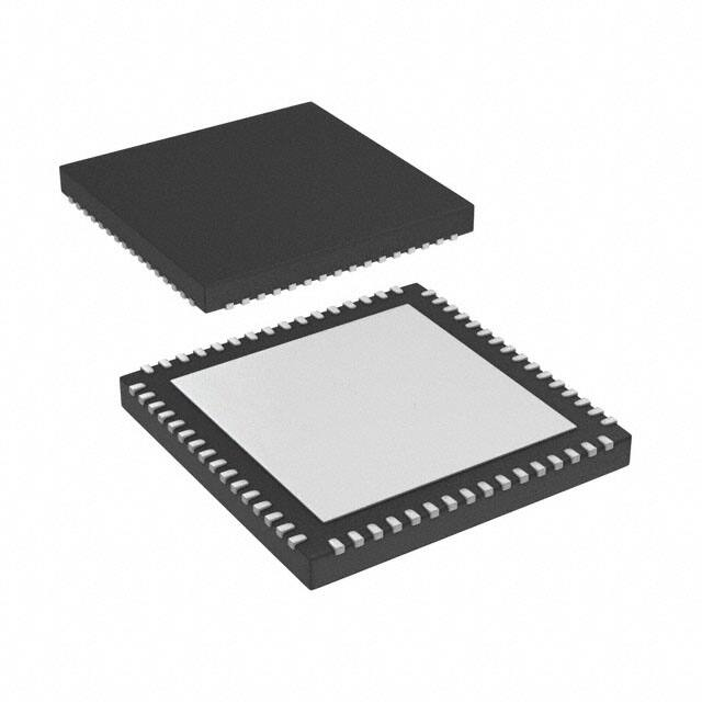


 工商网监
湘ICP备2023018690号
工商网监
湘ICP备2023018690号
