Product
Folder
Sample &
Buy
Support &
Community
Tools &
Software
Technical
Documents
ADS5400
SLAS611C – OCTOBER 2009 – REVISED JANUARY 2016
ADS5400 12-Bit, 1-GSPS Analog-to-Digital Converter
1 Features
3 Description
•
•
•
•
•
•
•
The ADS5400 device is a 12-bit, 1-GSPS analog-todigital converter (ADC) that operates from both a 5-V
supply and 3.3-V supply, while providing LVDScompatible digital outputs. The analog input buffer
isolates the internal switching of the track and hold
from disturbing the signal source. The simple 3-stage
pipeline provides extremely low latency for time
critical applications. Designed for the conversion of
signals up to 2 GHz of input frequency at 1 GSPS,
the ADS5400 has outstanding low noise performance
and spurious-free dynamic range over a large input
frequency range.
1
•
•
•
•
•
•
1-GSPS Sample Rate
12-Bit Resolution
2.1 GHz Input Bandwidth
SFDR = 66 dBc at 1.2 GHz
SNR = 57.6 dBFS at 1.2 GHz
7 Clock Cycle Latency
Interleave Friendly: Internal Adjustments for Gain,
Phase, and Offset
1.5-V to 2-V Selectable Full-Scale Range
LVDS-Compatible Outputs, 1 or 2 Bus Options
Total Power Dissipation: 2.15 W
On-Chip Analog Buffer
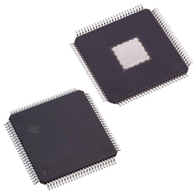
100-Pin HTQFP PowerPAD™ Package
(16-mm × 16-mm Footprint With Leads)
Industrial Temperature Range of –40°C to 85°C
The ADS5400 is available in a HTQFP-100
PowerPAD™ package. The combination of the
PowerPAD
package
and
moderate
power
consumption of the ADS5400 allows for operation
without an external heatsink. The ADS5400 is built on
Texas Instrument's complementary bipolar process
(BiCom3) and is specified over the full industrial
temperature range (–40°C to 85°C).
2 Applications
•
•
•
•
•
•
Device Information(1)
Test and Measurement Instrumentation
Ultra-Wide Band Software-Defined Radio
Data Acquisition
Power Amplifier Linearization
Signal Intelligence and Jamming
Radar
PART NUMBER
ADS5400
PACKAGE
HTQFP (100)
BODY SIZE (NOM)
14.00 mm × 14.00 mm
(1) For all available packages, see the orderable addendum at
the end of the datasheet.
Block Diagram
ADS5400
CLKINP
RESETP (SYNCINP)
RESETN (SYNCINN)
CLOCK
DIVIDE
CLKINN
INP
12
BUFFER
CLKOUTAP
12-bit ADC
(3 stage pipeline)
CLKOUTAN
INN
12
BUS A
VCM
VREF
SDO
SDENB
ENEXTREF
ENPWD
ENA1BUS
OUTA[0-11]N
OVRAP (SYNCOUTAP )
REFERENCE
SCLK
SDIO
OUTA [0-11]P
GAIN ADJUST
OVER RANGE
DETECTOR,
SYNC and
DEMUX
OVRAN (SYNCOUTAN)
CLKOUTBP
CLKOUTBN
PHASE ADJUST
CONTROL
12
BUS B
OFFSET ADJUST
OUTB[0-11]P
OUTB[0-11]N
OVRBP (SYNCOUTBP)
TEMP SENSOR
OVRBN (SYNCOUTBN)
1
An IMPORTANT NOTICE at the end of this data sheet addresses availability, warranty, changes, use in safety-critical applications,
intellectual property matters and other important disclaimers. PRODUCTION DATA.
�ADS5400
SLAS611C – OCTOBER 2009 – REVISED JANUARY 2016
www.ti.com
Table of Contents
1
2
3
4
5
6
Features ..................................................................
Applications ...........................................................
Description .............................................................
Revision History.....................................................
Pin Configuration and Functions .........................
Specifications.........................................................
6.1
6.2
6.3
6.4
6.5
6.6
6.7
6.8
6.9
7
1
1
1
2
4
6
Absolute Maximum Ratings ...................................... 6
ESD Ratings.............................................................. 6
Recommended Operating Conditions....................... 7
Thermal Information .................................................. 7
Electrical Characteristics........................................... 7
Interleaving Adjustments........................................... 9
Timing Requirements ............................................. 10
Switching Characteristics ........................................ 12
Typical Characteristics ............................................ 18
Detailed Description ............................................ 22
7.1 Overview ................................................................. 22
7.2 Functional Block Diagram ....................................... 22
7.3 Feature Description................................................. 22
7.4 Device Functional Modes........................................ 28
7.5 Programming........................................................... 29
7.6 Register Maps ......................................................... 31
8
Application and Implementation ........................ 39
8.1 Application Information............................................ 39
8.2 Typical Application .................................................. 39
9 Power Supply Recommendations...................... 43
10 Layout................................................................... 44
10.1 Layout Guidelines ................................................. 44
10.2 Layout Example .................................................... 44
10.3 PowerPAD™ Package .......................................... 45
11 Device and Documentation Support ................. 46
11.1
11.2
11.3
11.4
11.5
11.6
Device Support......................................................
Documentation Support ........................................
Community Resources..........................................
Trademarks ...........................................................
Electrostatic Discharge Caution ............................
Glossary ................................................................
46
47
47
47
47
47
12 Mechanical, Packaging, and Orderable
Information ........................................................... 47
4 Revision History
NOTE: Page numbers for previous revisions may differ from page numbers in the current version.
Changes from Revision B (March 2010) to Revision C
Page
•
Added Pin Configuration and Functions section, ESD Ratings table, Feature Description section, Device Functional
Modes, Application and Implementation section, Power Supply Recommendations section, Layout section, Device
and Documentation Support section, and Mechanical, Packaging, and Orderable Information section .............................. 1
•
Deleted Thermal Characteristics table ................................................................................................................................... 6
Changes from Revision A (November 2009) to Revision B
Page
•
Changed Data sheet From: Product Preview To: Production ................................................................................................ 1
•
Changed INL - Integral non- linearity error Max value From: 4 To: 4.5 ................................................................................. 7
•
Changed Worst harmonic/spur (other than HD2 and HD3), fIN = 1200 MHz TYP value From: 70 To 66.............................. 9
•
Changed Worst harmonic/spur (other than HD2 and HD3), fIN = 1700 MHz TYP value From: 66 To 64.............................. 9
•
Changed Total Harmonic Distortion, fIN = 125 MHz TYP value From: 73.5 To 71.7.............................................................. 9
•
Changed Total Harmonic Distortion, fIN = 600 MHz TYP value From: 68.5 To 67................................................................. 9
•
Changed Total Harmonic Distortion, fIN = 850 MHz TYP value From: 68.5 To 66.5.............................................................. 9
•
Changed Total Harmonic Distortion, fIN = 1700 MHz TYP value From: 56.2 To 55.7............................................................ 9
•
Changed Signal-to-noise and distortion, fIN = 125 MHz TYP value From: 58 To 58.5........................................................... 9
•
Changed Signal-to-noise and distortion, fIN = 600 MHz TYP value From: 57.4 To 58.2........................................................ 9
•
Changed Signal-to-noise and distortion, fIN = 850 MHz TYP value From: 57.3 To 57.8........................................................ 9
•
Changed Signal-to-noise and distortion, fIN = 1200 MHz TYP value From: 57.2 To 57.5...................................................... 9
•
Changed Signal-to-noise and distortion, fIN = 1700 MHz TYP value From: 54 To 54.2......................................................... 9
•
Changed Effective number of bits (using SINAD in dBFS), fIN = 125 MHz TYP value From: 9.34 To 9.42 .......................... 9
•
Changed Effective number of bits (using SINAD in dBFS), fIN = 600 MHz TYP value From: 9.24 To 9.37 .......................... 9
•
Changed Effective number of bits (using SINAD in dBFS), fIN = 850 MHz TYP value From: 9.23 To 9.3 ............................ 9
•
Changed INPUT CLOCK COARSE PHASE ADJUSTMENT, Integral Non-Linearity error Max value From: 4 To 5 .......... 10
2
Submit Documentation Feedback
Copyright © 2009–2016, Texas Instruments Incorporated
Product Folder Links: ADS5400
�ADS5400
www.ti.com
SLAS611C – OCTOBER 2009 – REVISED JANUARY 2016
•
Changed Table 5, BIT 4 From: 1 To: 0 ................................................................................................................................ 32
•
Deleted note: (was not available on early samples) from SPI Register Reset in Table 5.................................................... 32
Changes from Original (October 2009) to Revision A
Page
•
Changed the FEATURES list ................................................................................................................................................. 1
•
Deleted text "Internal pull-down resistor" from the SCLK, SDIO, and SDO pins in the Pin Functions table ......................... 5
•
Changed the SDENB pin text From: "Internal pull-up resistor" To: "Internal 100kΩ pull-up resisto" in the Pin
Functions table ....................................................................................................................................................................... 5
•
Added Note to the Pin Functions table - This pin contains an internal ~40kΩ pull-down resistor, to ground. ....................... 5
•
Changed Abs Max, Recommended Op Conditions, and Electrical Specs values. ............................................................... 6
•
Changed the description of the ANALOG INPUT entry in the Rec Op Condition table From: Differential input range
To: Full-scale differential input range ..................................................................................................................................... 7
•
Changed the Rec Op table, VCM - TYP value From: 2.5V To AVDD5/2 ................................................................................ 7
•
Changed the description of the ANALOG INPUT entry in the Elect Char table From: Differential input range To: Fullscale differential input range................................................................................................................................................... 7
•
Changed the Elect Char table, VCM - TYP value From: 2.5V To AVDD5/2............................................................................ 7
•
Changed the Timing Diagrams illustrations.......................................................................................................................... 13
•
Changed Figure 1................................................................................................................................................................. 13
•
Changed Figure 2................................................................................................................................................................. 14
•
Changed Figure 3................................................................................................................................................................. 15
•
Changed Figure 4................................................................................................................................................................. 16
•
Changed Figure 5................................................................................................................................................................. 17
•
Changed the TYPICAL CHARACTERISTICS, Conditions Note From: DVDD3 = 3.3 V, and 3.3-VPP differential clock
To: DVDD = 3.3V and 1.5 VPP differential clock ................................................................................................................... 18
•
Added subsection - Analog Input Over-Range Recovery Error............................................................................................ 24
•
Changed the Clock Inputs subsection .................................................................................................................................. 24
•
Changed the Test Patterns subsection ................................................................................................................................ 27
•
Changed the Interleaving subsection ................................................................................................................................... 28
•
Changed Table 6 BIT , Title and description............................................................................................................... 33
•
Changed Table 7 BIT , Default setting description, and BIT description ............................................................. 33
•
Changed Table 8 BIT , Default setting description ........................................................................................................ 34
•
Changed Serial Register 0x06 (Read or Write) (Table 10). Bits 4 and 5 From TBD To: 0.................................................. 36
•
Deleted Table 10 description comment from BIT 11: (this mode is not working properly on early samples - will
be fixed) ................................................................................................................................................................................ 36
•
Changed the Power Supplies subsection............................................................................................................................. 43
•
Added Figure 40 - Was TBD ................................................................................................................................................ 43
Submit Documentation Feedback
Copyright © 2009–2016, Texas Instruments Incorporated
Product Folder Links: ADS5400
3
�ADS5400
SLAS611C – OCTOBER 2009 – REVISED JANUARY 2016
www.ti.com
5 Pin Configuration and Functions
1
76
77
78
79
80
81
82
83
84
85
86
87
88
89
90
91
92
93
94
95
96
97
98
99
75
2
74
3
73
4
72
5
71
6
70
7
69
8
68
9
67
10
66
11
65
12
64
ADS5400
(TOP VIEW)
13
63
14
62
15
61
16
60
17
59
18
58
19
57
20
56
21
55
54
22
23
53
Thermal Pad = AGND
50
49
48
47
46
45
44
43
42
41
40
39
38
37
36
35
34
33
32
31
30
DA11P
DA11N
DA10P
DA10N
DA9P
DA9N
DA8P
DA8N
DA7P
DA7N
DGND
DVDD3
DA6P
DA6N
CLKOUTAP
CLKOUTAN
DA5P
DA5N
DA4P
DA4N
DA3P
DA3N
DA2P
DA2N
DGND
CLKOUTBN
CLKOUTBP
DB5N
DB5P
DB4N
DB4P
DB3N
DB3P
DB2N
DB2P
DB1N
DB1P
DVDD3
DGND
DB0N
DB0P
OVRBN
OVRBP
OVRAN
OVRAP
DA0N
DA0P
DA1N
DA1P
DVDD3
29
51
28
52
25
27
24
26
AVDD5
AVDD3
AGND
CLKINP
CLKINN
AGND
AVDD3
AGND
AVDD3
RESETN
RESETP
DB11N
DB11P
DB10N
DB10P
DB9N
DB9P
DB8N
DB8P
DB7N
DB7P
DB6N
DB6P
DVDD3
DGND
100
AGND
AVDD5
AGND
AVDD5
AGND
AINN
AINP
AGND
AVDD5
AGND
AVDD5
VCM
AGND
VREF
AVDD5
AVDD3
AGND
ENEXTREF
ENPWD
ENA1BUS
SDO
SDIO
SCLK
SDENB
AVDD5
PZP Package
100-Pin HTQFP With Exposed Thermal Pad
Top View
4
Submit Documentation Feedback
Copyright © 2009–2016, Texas Instruments Incorporated
Product Folder Links: ADS5400
�ADS5400
www.ti.com
SLAS611C – OCTOBER 2009 – REVISED JANUARY 2016
Pin Functions
PIN
TYPE
DESCRIPTION
NO.
NAME
3, 6, 8,
84, 88,
91, 93,
96, 98,
100
AGND
Ground
94, 95
AINP, AINN
Input
2, 7, 9,
85
AVDD3
Supply
Analog power supply (3.3 V)
1, 76, 86,
90, 92,
97, 99
AVDD5
Supply
Analog power supply (5 V)
CLKINP, CLKINN
Input
60, 61
CLKOUTAN,
CLKOUTAP
Output
Bus A, Clock output (Data ready), LVDS output pair
26, 27
CLKOUTBN,
CLKOUTBP
Output
Bus B, Clock output (Data ready), LVDS output pair
46, 47
DA0N, DA0P
Output
Bus A, LVDS digital output pair, least-significant bit (LSB) (P = positive output, N =
negative output)
48-49,
52-59,
62-63,
66-73
DA1N–DA10N,
DA1P-DA10P
Output
Bus A, LVDS digital output pairs (bits 1- 10)
74, 75
DA11N, DA11P
Output
Bus A, LVDS digital output pair, most-significant bit (MSB)
40, 41
DB0N, DB0P
Output
Bus B, LVDS digital output pair, least-significant bit (LSB) (P = positive output, N =
negative output)
14-23,
28-37
DB1N–DB10N,
DB1P-DB10P
Output
Bus B, LVDS digital output pairs (bits 1- 10)
12, 13
DB11N, DB11P
Output
Bus B, LVDS digital output pair, most-significant bit (MSB)
25, 39,
51, 65
DGND
Ground
Digital ground
24, 38,
50, 64
DVDD3
Supply
Output driver power supply (3.3 V)
81 (1)
ENA1BUS
Input
Enable single output bus mode (2-bus mode is default), active high. This pin is logic
OR'd with addr 0x02h bit.
83 (1)
ENEXTREF
Input
Enable External Reference Mode, active high. Device uses an external voltage reference
when high. This pin is logic OR'd with addr 0x05h bit.
82 (1)
ENPWD
Input
Enable Powerdown, active high. Places the converter into power-saving sleep mode
when high. This pin is logic OR'd with addr 0x05h bit.
44, 45
OVRAN, OVRAP
Output
Bus A, Overrange indicator LVDS output. A logic high signals an analog input in excess
of the full-scale range. Becomes SYNCOUTA when SYNC mode is enabled in register
0x05.
42, 43
OVRBN, OVRBP
Output
Bus B, Overrange indicator LVDS output. A logic high signals an analog input in excess
of the full-scale range. Becomes SYNCOUTB when SYNC mode is enabled in register
0x05.
4, 5
Analog ground
Analog differential input signal (positive, negative). Includes 100-Ω differential load onchip.
Differential input clock (positive, negative). Includes 160-Ω differential load on-chip.
RESETN,
RESETP
Input
Digital Reset Input, LVDS input pair. Inactive if logic low. When clocked in a high state,
this is used for resetting the polarity of CLKOUT signal pair(s). If SYNC mode is enabled
in register 0x05, this input also provides a SYNC time-stamp with the data sample
present when RESET is clocked by the ADC, as well as CLKOUT polarity reset. Includes
100-Ω differential load on-chip.
78
SCLK
Input
Serial interface clock.
77
SDENB
Input
Active low serial data enable, always an input. Use to enable the serial interface. Internal
100kΩ pull-up resistor.
79
SDIO
Input/Output
10, 11
(1)
Bidirectional serial interface data in 3-pin mode (default) for programming/reading
internal registers. In 4-pin interface mode (reg 0x01), the SDIO pin is an input only.
This pin contains an internal ~40kΩ pull-down resistor, to ground.
Submit Documentation Feedback
Copyright © 2009–2016, Texas Instruments Incorporated
Product Folder Links: ADS5400
5
�ADS5400
SLAS611C – OCTOBER 2009 – REVISED JANUARY 2016
www.ti.com
Pin Functions (continued)
PIN
NO.
TYPE
NAME
80
SDO
Output
89
VCM
Input/Output
87
VREF
Input
DESCRIPTION
Unidirectional serial interface data in 4-pin mode (reg 0x01) provides internal register
settings. The SDO pin is in high-impedance state in 3-pin interface mode (default).
Analog input common mode voltage, Output (for DC-coupled applications, nominally 2.5
V). A 0.1-μF capacitor to AGND is recommended, but not required.
Reference voltage input (2 V nominal). A 0.1-μF capacitor to AGND is recommended,
but not required.
6 Specifications
6.1 Absolute Maximum Ratings
over operating free-air temperature range (unless otherwise noted) (1)
MAX
UNIT
AVDD5 to GND
MIN
6
V
AVDD3 to GND
5
V
DVDD3 to GND
5
V
0.5
4.5
V
Short duration
–0.3
(AVDD5 +
0.3)
V
Continuous AC signal
1.25
3.75
V
Continuous DC signal
1.75
3.25
V
AINP, AINN to GND (2)
Supply
voltage
Voltage difference between pin and ground
Voltage difference
between pins, common
mode at AVDD5/2
AINP to AINN (2)
Pin voltage
CLKINP, CLKINN to GND (2)
Voltage difference between pin and ground
0.5
4.5
V
Continuous AC signal
1.1
3.9
V
CLKINP to CLKINN (2)
Voltage difference
between pins, common
mode at AVDD5/2
Continuous DC signal
2
3
V
RESETP, RESETN to
GND (2)
Voltage difference between pin and ground
–0.3
(AVDD5 +
0.3)
V
RESETP to RESETN (2)
Voltage difference
between pins
Continuous AC signal
1.1
3.9
V
Continuous DC signal
2
3
V
–0.3
(DVDD3 +
0.3)
–0.3
(AVDD3 +
0.3)
ENA1BUS, ENPWD,
ENEXTREF to GND (2)
–0.3
(AVDD5 +
0.3)
Operating
–40
Data/OVR Outputs to
GND (2)
SDENB, SDIO, SCLK to
GND (2)
Temperature
Voltage difference between pin and ground
Maximum junction , TJ
Storage, Tstg
(1)
(2)
–65
V
85
°C
150
°C
150
°C
Stresses above these ratings may cause permanent damage. Exposure to absolute maximum conditions for extended periods may
degrade device reliability. These are stress ratings only, and functional operation of the device at these or any other conditions beyond
those specified is not implied. Kirkendall voidings and current density information for calculation of expected lifetime is available upon
request.
Valid when supplies are within recommended operating range.
6.2 ESD Ratings
VALUE
V(ESD)
(1)
(2)
6
Electrostatic
discharge
Human body model (HBM), per ANSI/ESDA/JEDEC JS-001
(1)
2000
Charged device model (CDM), per JEDEC specification JESD22-C101 (2)
500
UNIT
V
JEDEC document JEP155 states that 500-V HBM allows safe manufacturing with a standard ESD control process.
JEDEC document JEP157 states that 250-V CDM allows safe manufacturing with a standard ESD control process.
Submit Documentation Feedback
Copyright © 2009–2016, Texas Instruments Incorporated
Product Folder Links: ADS5400
�ADS5400
www.ti.com
SLAS611C – OCTOBER 2009 – REVISED JANUARY 2016
6.3 Recommended Operating Conditions
MIN
NOM
MAX
UNIT
SUPPLIES
Analog supply voltage, AVDD5
4.75
5
5.25
V
Analog supply voltage, AVDD3
3.135
3.3
3.465
V
Digital supply voltage, DVDD3
3.135
3.3
3.465
V
ANALOG INPUT
Full-scale differential input range
VCM
1.52
Input common mode
2
VPP
AVDD5/2
V
DIGITAL OUTPUT
Differential output load
5
pF
CLOCK INPUT
CLK input sample rate (sine wave)
100
1000
Clock amplitude, differential
0.6
1.5
Clock duty cycle
TA
45%
Open free-air temperature
50%
–40
MSPS
VPP
55%
85
°C
6.4 Thermal Information
ADS5400
THERMAL METRIC (1)
PZP (HTQFP)
UNIT
100 PINS
RθJA
Junction-to-ambient thermal resistance
34.5
°C/W
RθJC(top)
Junction-to-case (top) thermal resistance
7.4
°C/W
RθJB
Junction-to-board thermal resistance
9.1
°C/W
ψJT
Junction-to-top characterization parameter
0.2
°C/W
ψJB
Junction-to-board characterization parameter
9
°C/W
RθJC(bot)
Junction-to-case (bottom) thermal resistance
0.4
°C/W
(1)
For more information about traditional and new thermal metrics, see the Semiconductor and IC Package Thermal Metrics application
report, SPRA953.
6.5 Electrical Characteristics
Typical values at TA = 25°C, minimum and maximum values over full temperature range TMIN = –40°C to TMAX = 85°C,
sampling rate = 1 GSPS, 50% clock duty cycle, AVDD5 = 5 V, AVDD3 = 3.3 V, DVDD3 = 3.3 V, –1-dBFS differential input,
and 1.5 VPP differential clock (unless otherwise noted)
PARAMETER
TEST CONDITIONS
MIN
TYP
MAX
UNIT
ANALOG INPUTS
Full-scale differential input range
Programmable
1.52
2
VPP
VCM
Common-mode input
Self-biased to AVDD5 / 2
RIN
Input resistance, differential (DC)
CIN
Input capacitance
Estimated to ground from each AIN pin,
excluding soldered package
0.8
pF
CMRR
Common-mode rejection ratio
Common mode signal = 125 MHz
40
dB
2
V
AVDD5/2
85
100
V
Ω
115
INTERNAL REFERENCE VOLTAGE
VREF
Reference voltage
DYNAMIC ACCURACY
Resolution
No missing codes
12
DNL
Differential linearity error
fIN = 125 MHz
–1
±0.7
2
LSB
INL
Integral non- linearity error
fIN = 125 MHz
–4
±2
4.5
LSB
Offset error
default is trimmed near 0 mV
–2.5
0
2.5
Offset temperature coefficient
Bits
0.02
mV
mV /°C
Submit Documentation Feedback
Copyright © 2009–2016, Texas Instruments Incorporated
Product Folder Links: ADS5400
7
�ADS5400
SLAS611C – OCTOBER 2009 – REVISED JANUARY 2016
www.ti.com
Electrical Characteristics (continued)
Typical values at TA = 25°C, minimum and maximum values over full temperature range TMIN = –40°C to TMAX = 85°C,
sampling rate = 1 GSPS, 50% clock duty cycle, AVDD5 = 5 V, AVDD3 = 3.3 V, DVDD3 = 3.3 V, –1-dBFS differential input,
and 1.5 VPP differential clock (unless otherwise noted)
PARAMETER
TEST CONDITIONS
Gain error
MIN
TYP
–5
Gain temperature coefficient
MAX
UNIT
5 % full scale
0.03
% full scale
/°C
POWER SUPPLY (1)
I(AVDD5)
I(AVDD3)
I(DVDD3)
5-V analog supply current (Bus A and fIN = 125 MHz,
B active)
fS = 1 GSPS
220
234
mA
5-V analog supply current (Bus A
active)
fIN = 125 MHz,
fS = 1 GSPS
225
241
mA
3.3-V analog supply current (Bus A
and B active)
fIN = 125 MHz,
fS = 1 GSPS
219
234
mA
3.3-V analog supply current (Bus A
active)
fIN = 125 MHz,
fS = 1 GSPS
226
242
mA
3.3-V digital supply current
(Bus A and B active)
fIN = 125 MHz,
fS = 1 GSPS
136
154
mA
3.3-V digital supply current
(Bus A active)
fIN = 125 MHz,
fS = 1 GSPS
71
81
mA
Total power dissipation
(BUS A and B active)
fIN = 125 MHz,
fS = 1 GSPS
2.28
2.45
W
Total power dissipation
(Bus A active)
fIN = 125 MHz,
fS = 1 GSPS
2.15
2.25
W
Total power dissipation
ENPWD = logic High (sleep enabled)
13
50
Wake-up time from sleep
PSRR
Power-supply rejection ratio
1MHz injected to each supply,
measured without external decoupling
mW
1.8
ms
50
dB
DYNAMIC AC CHARACTERISTICS
SNR
SFDR
Signal-to-noise ratio
Spurious-free dynamic range
fIN = 125 MHz
57
58.5
fIN = 600 MHz
56.5
58.2
fIN = 850 MHz
56
57.8
fIN = 1200 MHz
57.6
fIN = 1700 MHz
55.7
fIN = 125 MHz
65
75
fIN = 600 MHz
63
72
fIN = 850 MHz
60
71
fIN = 1200 MHz
HD3
(1)
8
Second harmonic
Third harmonic
dBc
66
fIN = 1700 MHz
HD2
dBFS
56
fIN = 125 MHz
65
78
fIN = 600 MHz
63
78
fIN = 850 MHz
60
71
fIN = 1200 MHz
66
fIN = 1700 MHz
56
fIN = 125 MHz
65
80
fIN = 600 MHz
63
72
fIN = 850 MHz
60
72
fIN = 1200 MHz
70
fIN = 1700 MHz
65
dBc
dBc
All power values assume LVDS output current is set to 3.5 mA.
Submit Documentation Feedback
Copyright © 2009–2016, Texas Instruments Incorporated
Product Folder Links: ADS5400
�ADS5400
www.ti.com
SLAS611C – OCTOBER 2009 – REVISED JANUARY 2016
Electrical Characteristics (continued)
Typical values at TA = 25°C, minimum and maximum values over full temperature range TMIN = –40°C to TMAX = 85°C,
sampling rate = 1 GSPS, 50% clock duty cycle, AVDD5 = 5 V, AVDD3 = 3.3 V, DVDD3 = 3.3 V, –1-dBFS differential input,
and 1.5 VPP differential clock (unless otherwise noted)
PARAMETER
TEST CONDITIONS
fIN = 125 MHz
fIN = 600 MHz
Worst harmonic/spur (other than HD2
fIN = 850 MHz
and HD3)
fIN = 1200 MHz
MIN
TYP
65
80
63
72
60
72
Total Harmonic Distortion
fIN = 125 MHz
63
fIN = 600 MHz
62
71.7
67
fIN = 850 MHz
59
66.5
Two-tone SFDR
ENOB
Effective number of bits (using
SINAD in dBFS)
RMS idle-channel noise
dBc
65.1
fIN = 1700 MHz
Signal-to-noise and distortion
dBc
64
fIN = 1200 MHz
SINAD
UNIT
66
fIN = 1700 MHz
THD
MAX
55.7
fIN = 125 MHz
56
58.5
fIN = 600 MHz
55
58.2
fIN = 850 MHz
54
57.8
fIN = 1200 MHz
57.5
fIN = 1700 MHz
54.2
fIN1 = 247.5 MHz, fIN2 = 252.5 MHz,
each tone at –7 dBFS
74.6
fIN1 = 247.5 MHz, fIN2 = 252.5 MHz,
each tone at –11 dBFS
80.4
dBFS
dBFS
fIN1 = 1197.5 MHz, fIN2 = 1202.5 MHz,
each tone at –7 dBFS
70
fIN1 = 1197.5 MHz, fIN2 = 1202.5 MHz,
each tone at –11 dBFS
78.3
fIN = 125 MHz
9
9.42
fIN = 600 MHz
8.84
9.37
fIN = 850 MHz
8.67
9.3
Inputs tied to common-mode
Bits
1.41
LSB rms
60.2
dBFS
6.6 Interleaving Adjustments
Typical values at TA = 25°C, Minimum and maximum values over full temperature range TMIN = –40°C to TMAX = 85°C,
sampling rate = 1 GSPS, 50% clock duty cycle, AVDD5 = 5 V, AVDD3 = 3.3 V, DVDD3 = 3.3 V, and 1.5 VPP differential clock
(unless otherwise noted)
PARAMETER
TEST CONDITIONS
MIN
TYP
MAX
UNIT
OFFSET ADJUSTMENTS
Resolution
LSB magnitude
DNL
Differential linearity error
INL
Integral Non-Linearity error
9
At full scale range of 2 VPP
Bits
120
µV
-2.5
2.5
LSB
-3
3
LSB
Recommended Min Offset
Setting
From default offset value, to maintain AC
performance
-8
mV
Recommended Max Offset
Setting
From default offset value, to maintain AC
performance
8
mV
GAIN ADJUSTMENTS
Resolution
12
LSB magnitude
Bits
120
Submit Documentation Feedback
Copyright © 2009–2016, Texas Instruments Incorporated
Product Folder Links: ADS5400
µV
9
�ADS5400
SLAS611C – OCTOBER 2009 – REVISED JANUARY 2016
www.ti.com
Interleaving Adjustments (continued)
Typical values at TA = 25°C, Minimum and maximum values over full temperature range TMIN = –40°C to TMAX = 85°C,
sampling rate = 1 GSPS, 50% clock duty cycle, AVDD5 = 5 V, AVDD3 = 3.3 V, DVDD3 = 3.3 V, and 1.5 VPP differential clock
(unless otherwise noted)
MIN
TYP
MAX
UNIT
DNL
Differential linearity error
PARAMETER
TEST CONDITIONS
-4
-2, +1
4
LSB
INL
Integral Non-Linearity error
-8
-2, +4
8
LSB
Min Gain Setting
1.52
VPP
Max Gain Setting
2
VPP
INPUT CLOCK FINE PHASE ADJUSTMENT
Resolution
6
Bits
LSB magnitude
DNL
Differential linearity error
INL
Integral Non-Linearity error
116
fs
-2
-2.5
Max Fine Clock Skew setting
2.5
LSB
4
LBS
7.4
ps
INPUT CLOCK COARSE PHASE ADJUSTMENT
Resolution
5
Bits
LSB magnitude
2.4
ps
DNL
Differential linearity error
-1
1
LSB
INL
Integral Non-Linearity error
-1
5
LSB
Max Coarse Clock Skew
setting
73
ps
6.7 Timing Requirements
Typical values at TA = 25°C, Minimum and maximum values over full temperature range TMIN = –40°C to TMAX = 85°C,
sampling rate = 1 GSPS, 50% clock duty cycle, AVDD5 = 5 V, AVDD3 = 3.3 V, DVDD3 = 3.3 V, and 1.5 VPP differential clock
(unless otherwise noted) (1).
MIN
ta
Aperture delay
Aperture jitter, rms
Uncertainty of sample point due to internal jitter
sources
Bus A, using Single Bus Mode
Latency
NOM MAX
UNIT
250
ps
125
fs
7
Bus A, using Dual Bus Mode Aligned
7.5
Bus B, using Dual Bus Mode Aligned
8.5
Bus A and B, using Dual Bus Mode Staggered
7.5
Cycles
LVDS OUTPUT TIMING (DATA, CLKOUT, OVR/SYNCOUT) (2)
tCLK
Clock period
tCLKH
Clock pulse duration, high
Assuming worst case 45/55 duty cycle
0.45
tCLKL
Clock pulse duration, low
Assuming worst case 55/45 duty cycle
0.45
tPD-CLKDIV2
Clock propagation delay
CLKIN rising to CLKOUT rising in divide by 2 mode
700
1200 1700
ps
tPD-CLKDIV4
Clock propagation delay
CLKIN rising to CLKOUT rising in divide by 4 mode
700
1200 1700
ps
tPD-ADATA
Bus A data propagation
delay
CLKIN falling to Data Output transition
700
1400 2100
ps
tPD-BDATA
Bus B data propagation
delay
CLKIN falling to Data Output transition
700
1400 2100
ps
Setup time, single bus mode
Data valid to CLKOUT edge, 50% CLKIN duty cycle
tSU-SBM
(1)
(2)
(3)
10
(3)
1
290p
10
ns
ns
ns
(tCLK/2) 185p
s
Timing parameters are specified by design or characterization, but not production tested.
LVDS output timing measured with a differential 100-Ω load placed ~4 inches from the ADS5400. Measured differential load capacitance
is 3.5 pF. Measurement probes and other parasitics add ~1 pF. Total approximate capacitive load is 4.5 pF differential. All timing
parameters are relative to the device pins, with the loading as stated.
In single bus mode at 1 GSPS (1-ns clock), the minimum output setup/hold times over process and temperature provide a minimum 700
ps of data valid window, with 300 ps of uncertainity.
Submit Documentation Feedback
Copyright © 2009–2016, Texas Instruments Incorporated
Product Folder Links: ADS5400
�ADS5400
www.ti.com
SLAS611C – OCTOBER 2009 – REVISED JANUARY 2016
Timing Requirements (continued)
Typical values at TA = 25°C, Minimum and maximum values over full temperature range TMIN = –40°C to TMAX = 85°C,
sampling rate = 1 GSPS, 50% clock duty cycle, AVDD5 = 5 V, AVDD3 = 3.3 V, DVDD3 = 3.3 V, and 1.5 VPP differential clock
(unless otherwise noted)(1).
MIN
NOM MAX
UNIT
tH-SBM
Hold time, single bus mode
CLKOUT edge to Data invalid, 50% CLKIN duty
cycle
410p
(tCLK/2) 65p
s
tSU-DBM
Setup time, dual bus mode
Data valid to CLKOUT edge, 50% CLKIN duty cycle
550p
tCLK 425p
s
tH-DBM
Hold time, dual bus mode
CLKOUT edge to Data invalid, 50% CLKIN duty
cycle
1150p
tCLK +
175p
s
tr
LVDS rise time
Measured 20% to 80%
400
ps
tf
LVDS output fall time
Measured 20% to 80%
400
ps
LVDS INPUT TIMING (RESETIN)
tRSU
RESET setup time
RESETP going HIGH to CLKINP going LOW
300
tRH
RESET hold time
CLKINP going LOW to RESETP going LOW
300
RESET input capacitance
Differential
RESET input current
ps
ps
1
pF
±1
µA
SERIAL INTERFACE TIMING
tS-SDENB
Setup time, serial enable
SDENB falling to SCLK rising
20
ns
tH-SDENB
Hold time, serial enable
SCLK falling to SENDB rising
25
ns
tS-SDIO
Setup time, SDIO
SDIO valid to SCLK rising
10
ns
tH-SDIO
Hold time, SDIO
SCLK rising to SDIO transition
10
fSCLK
Frequency
tSCLK
SCLK period
100
ns
tSCLKH
Minimum SCLK high time
40
ns
tSCLKL
Minimum SCLK low time
40
ns
tr
Rise time
10 pF
10
ns
tf
Fall time
10 pF
10
ns
Data output delay
Data output (SDO/SDIO) delay after SCLK falling,
10-pF load
tDDATA
ns
10
75
Submit Documentation Feedback
Copyright © 2009–2016, Texas Instruments Incorporated
Product Folder Links: ADS5400
MHz
ns
11
�ADS5400
SLAS611C – OCTOBER 2009 – REVISED JANUARY 2016
www.ti.com
6.8 Switching Characteristics
Typical values at TA = 25°C, Minimum and maximum values over full temperature range TMIN = –40°C to TMAX = 85°C,
sampling rate = 1 GSPS, 50% clock duty cycle, AVDD5 = 5 V, AVDD3 = 3.3 V, DVDD3 = 3.3 V, and 1.5 VPP differential clock
(unless otherwise noted)
PARAMETER
TEST CONDITIONS
MIN
TYP
MAX
UNIT
mV
LVDS DIGITAL OUTPUTS (DATA, OVR/SYNCOUT, CLKOUT)
VOD
Differential output voltage (±)
Terminated 100 Ω differential
247
350
454
VOC
Common mode output voltage
Terminated 100 Ω differential
1.125
1.25
1.375
V
LVDS DIGITAL INPUTS (RESET)
VID
Differential input voltage (±)
Each input pin
175
350
VIC
Common mode input voltage
Each input pin
0.1
1.25
2.4
V
RIN
Input resistance
85
100
115
Ω
CIN
Input capacitance
Each pin to ground
mV
0.6
pF
DIGITAL INPUTS (SCLK, SDIO, SDENB)
VIH
High level input voltage
2
AVDD3 + 0.3
VIL
Low level input voltage
0
0.8
V
IIH
High level input current
±1
μA
IIL
Low level input current
±1
μA
CIN
Input capacitance
2
pF
V
DIGITAL INPUTS ( ENEXTREF, ENPWD, ENA1BUS)
VIH
High level input voltage
2
AVDD5 + 0.3
VIL
Low level input voltage
0
0.8
V
IIH
High level input current
~40-kΩ internal pulldown
125
μA
IIL
Low level input current
~40-kΩ internal pulldown
20
μA
CIN
Input capacitance
2
pF
V
DIGITAL OUTPUTS (SDIO, SDO)
VOH
High level output voltage
IOH = 250 µA
VOL
Low level output voltage
IOL = 250 µA
2.8
V
0.4
V
190
Ω
CLOCK INPUTS
RIN
Differential input resistance
CLKINP, CLKINN
CIN
Input capacitance
Estimated to ground from each
CLKIN pin, excluding soldered
packaged
12
Submit Documentation Feedback
130
160
0.8
pF
Copyright © 2009–2016, Texas Instruments Incorporated
Product Folder Links: ADS5400
�ADS5400
www.ti.com
SLAS611C – OCTOBER 2009 – REVISED JANUARY 2016
DIFFERENTIAL
ANALOG INPUT
(INP-INN)
N
Aperture
delay
N+1
ta
N+2
Sample N and RESET pulse
captured here
N
output
tCLKH
N+1
output
tCLKL
CLKINP
tRSU
tRH
CLKOUT is reset after 3.5 CLKIN cycles (+ tPD-CLKDIV2 )
tPD-CLKDIV2
RESETP
Phase 0: CLKOUT in desired
CLKOUTAP state after power up
Phase 1: misaligned by
1 clock after power up
tPD-ADATA
tsu
Latency of N and SYNCOUTA are matched to 7 CLKIN cycles
N-1
DATA BUS A
SYNCOUTA
(OVRA pins)
If SYNC mode is enabled,
the OVRA pins become SYNCOUTA pins
th
N
N+1
N+2
Sync
Propagation delays and setup/hold times not drawn to scale. RESET and SYNCOUT are optional. Any clock phase
will work properly, but makes synchronization of data capture across multiple ADCs difficult without a known CLKOUT
phase. RESET can be a single pulse (as shown), low-to-high step or repetitive pulse input signal. The frequency of
repetitive RESET pulses should not exceed CLKIN/2, and should be an even divisor of CLKIN, to keep the CLKOUT
phase the same with each RESET event. SYNCOUTA transitions with the same latency as the sample that is present
when the RESET pulse is captured, shown here as sample N. Each RESET captured generates a SYNCOUT pulse,
which behaves as a data bit. Bus B is not active in single bus mode.
Figure 1. Single Bus Mode
Submit Documentation Feedback
Copyright © 2009–2016, Texas Instruments Incorporated
Product Folder Links: ADS5400
13
�ADS5400
SLAS611C – OCTOBER 2009 – REVISED JANUARY 2016
www.ti.com
Sample N and RESET
pulse captured here
N, N+1
output
N+1
CLKINP
tRSU
RESETP
tRH
CLKOUT is reset after 3.5 CLKIN cycles (+ tPD-CLKDIV2 )
tPD-CLKDIV2
CLKOUTAP
CLKOUTBP
Phase 0: CLKOUT in desired
state after power up
Phase 1: misaligned by 1
clock after power up
tPD-BDATA
tsu
Latency of N and SYNCOUTB are matched to 8.5 CLKIN cycles
DATA BUS B
The phase of data shown prior to reset matches CLKOUT in phase 0
SYNCOUTB
(OVRB pins)
If SYNC mode is enabled,
the OVRB pins become SYNCOUTB pins
DATA BUS A
The phase of data shown prior to reset matches CLKOUT in phase 0
Latency of N+1 is 7.5 CLKIN cycles
th
N
N+2
Sync
N+1
N+3
tPD-ADATA
Propagation delays and setup/hold times not drawn to scale. RESET and SYNCOUT are optional. Any clock phase
will work properly, but makes synchronization of data capture across multiple ADCs difficult without a known CLKOUT
phase. RESET can be a single pulse (as shown), low-to-high step or repetitive pulse input signal. The frequency of
repetitive RESET pulses should not exceed CLKIN/2, and should be an even divisor of CLKIN, to keep the CLKOUT
phase the same with each RESET event. SYNCOUTB transitions with the same latency as the sample that is present
when the RESET pulse is captured, shown here as sample N. Each RESET captured generates a SYNCOUT pulse,
which behaves as a data bit.
Figure 2. Dual Bus Mode - Aligned, CLKOUT Divide By 2
14
Submit Documentation Feedback
Copyright © 2009–2016, Texas Instruments Incorporated
Product Folder Links: ADS5400
�ADS5400
www.ti.com
SLAS611C – OCTOBER 2009 – REVISED JANUARY 2016
Sample N and RESET
pulse captured here
N
output
N+1
N+1
output
CLKINP
tRSU
tRH
CLKOUT is reset after 3.5 CLKIN cycles (+ tPD-CLKDIV2 )
RESETP
tPD-CLKDIV2
Phase 0: CLKOUT in desired
state after power up
CLKOUTAP
Phase 1: misaligned by 1
clock after power up
Phase 0: CLKOUT in desired
state after power up
CLKOUTBP
Phase 1: misaligned by 1
clock after power up
tPD-BDATA
tsu
Latency of N and SYNCOUTB are matched to 7.5 CLKIN cycles
DATA BUS B
The phase of data shown prior to reset matches CLKOUT in phase 0
If SYNC mode is enabled,
the OVRB pins become SYNCOUTB pins
SYNCOUTB
(OVRB pins)
DATA BUS A
th
N
N+2
Sync
N+1
The phase of data shown prior to reset matches CLKOUT in phase 0
Latency of N+1 is 7.5 CLKIN cycles
N+3
tPD-ADATA
Propagation delays and setup/hold times not drawn to scale. RESET and SYNCOUT are optional. Any clock phase
will work properly, but makes synchronization of data capture across multiple ADCs difficult without a known CLKOUT
phase. RESET can be a single pulse (as shown), low-to-high step or repetitive pulse input signal. The frequency of
repetitive RESET pulses should not exceed CLKIN/2, and should be an even divisor of CLKIN, to keep the CLKOUT
phase the same with each RESET event. SYNCOUTB transitions with the same latency as the sample that is present
when the RESET pulse is captured, shown here as sample N. Each RESET captured generates a SYNCOUT pulse,
which behaves as a data bit.
Figure 3. Dual Bus Mode - Staggered, CLKOUT Divide By 2
Submit Documentation Feedback
Copyright © 2009–2016, Texas Instruments Incorporated
Product Folder Links: ADS5400
15
�ADS5400
SLAS611C – OCTOBER 2009 – REVISED JANUARY 2016
www.ti.com
Sample N and RESET
pulse captured here
N, N+1
output
N+1
CLKINP
tRSU
RESETP
tRH
tPD-CLKDIV4
CLKOUT is reset after 7.5 CLKIN cycles (+ tPD-CLKDIV4 )
Phase 0: CLKOUT in desired
state after power up
CLKOUTAP
CLKOUTBP
Phase 1: misaligned by 1
clock after power up
Phase 2: misaligned by 2
clocks after power up
Phase 3: misaligned by 3
clocks after power up
tPD-BDATA
Latency of N and SYNCOUTB are matched to 8.5 CLKIN cycles
tsu
th
DATA BUS B
SYNCOUTB
(OVRB pins)
DATA BUS A
The phase of data shown prior to reset matches CLKOUT in phase 0
If SYNC mode is enabled,
the OVRB pins become SYNCOUTB pins
The phase of data shown prior to reset matches CLKOUT in phase 0
Latency of N+1 is 7.5 CLKIN cycles
N
Sync
N+1
tPD-ADATA
Propagation delays and setup/hold times not drawn to scale. RESET and SYNCOUT are optional. Any clock phase
will work properly, but makes synchronization of data capture across multiple ADCs difficult without a known CLKOUT
phase. RESET can be a single pulse (as shown), low-to-high step or repetitive pulse input signal. The frequency of
repetitive RESET pulses should not exceed CLKIN/4, and should be an even divisor of CLKIN, to keep the CLKOUT
phase the same with each RESET event. SYNCOUTB transitions with the same latency as the sample that is present
when the RESET pulse is captured, shown here as sample N. Each RESET captured generates a SYNCOUT pulse,
which behaves as a data bit.
Figure 4. Dual Bus Mode - Aligned, CLKOUT Divide By 4
16
Submit Documentation Feedback
Copyright © 2009–2016, Texas Instruments Incorporated
Product Folder Links: ADS5400
�ADS5400
www.ti.com
SLAS611C – OCTOBER 2009 – REVISED JANUARY 2016
Sample N and RESET
pulse captured here
N
output
N+1
sampled
N+1
output
CLKINP
tRSU
tRH
CLKOUTA is reset after 7.5 CLKIN cycles (+ tPD-CLKDIV4 )
RESETP
tPD-CLKDIV4
Phase 0: CLKOUT in desired
state after power up
Phase 1: misaligned by 1
clock after power up
CLKOUTAP
Phase 2: misaligned by 2
clocks after power up
Phase 3: misaligned by 3
clocks after power up
tPD-CLKDIV4
CLKOUTB is reset after 6.5 CLKIN cycles (+ tPD-CLKDIV4 )
Phase 0: CLKOUT in desired
state after power up
Phase 1: misaligned by 1
clock after power up
CLKOUTBP
Phase 2: misaligned by 2
clocks after power up
Phase 3: misaligned by 3
clocks after power up
tPD-BDATA
Latency of N and SYNCOUTB are matched to 7.5 CLKIN cycles
DATA BUS B
The phase of data shown prior to reset matches CLKOUTB in phase 0
If SYNC mode is enabled,
the OVRB pins become SYNCOUTB pins
SYNCOUTB
(OVRB pins)
DATA BUS A
tsu
th
N+2
N
Sync
The phase of data shown prior to reset matches CLKOUTA in phase 0
Latency of N+1 is 7.5 CLKIN cycles
N+1
tPD-ADATA
Propagation delays and setup/hold times not drawn to scale. RESET and SYNCOUT are optional. Any clock phase
will work properly, but makes synchronization of data capture across multiple ADCs difficult without a known CLKOUT
phase. RESET can be a single pulse (as shown), low-to-high step or repetitive pulse input signal. The frequency of
repetitive RESET pulses should not exceed CLKIN/4, and should be an even divisor of CLKIN, to keep the CLKOUT
phase the same with each RESET event. SYNCOUTB transitions with the same latency as the sample that is present
when the RESET pulse is captured, shown here as sample N. Each RESET captured generates a SYNCOUT pulse,
which behaves as a data bit.
Figure 5. Dual Bus Mode - Staggered, CLKOUT Divide By 4
Submit Documentation Feedback
Copyright © 2009–2016, Texas Instruments Incorporated
Product Folder Links: ADS5400
17
�ADS5400
SLAS611C – OCTOBER 2009 – REVISED JANUARY 2016
www.ti.com
6.9 Typical Characteristics
Typical plots at TA = 25°C, sampling rate = 1 GSPS, 50% clock duty cycle, AVDD5 = 5 V, AVDD3 = 3.3 V, DVDD3 = 3.3 V,
and 1.5-VPP differential clock, (unless otherwise noted)
0
0
ENOB = 9.45 Bits
SFDR = 75.4 dBc
SINAD = 58.7 dBFS
SNR = 58.8 dBFS
THD = 72.5 dBc
−10
−20
−20
−30
Amplitude − dB
Amplitude − dB
−30
−40
−50
−60
−40
−50
−60
−70
−70
−80
−80
−90
−90
−100
−100
0
ENOB = 9.31 Bits
SFDR = 71.5 dBc
SINAD = 57.8 dBFS
SNR = 58.04 dBFS
THD = 69.8 dBc
−10
50 100 150 200 250 300 350 400 450 500
0
50 100 150 200 250 300 350 400 450 500
f − Frequency − MHz
f − Frequency − MHz
G001
Figure 6. Spectral Performance FFT for 250-MHz Input
Signal
G002
Figure 7. Spectral Performance FFT for 0.9-GHz Input Signal
0
0
ENOB = 9.01 Bits
SFDR = 63.5 dBc
SINAD = 56 dBFS
SNR = 57.1 dBFS
THD = 61.7 dBc
−10
−20
−20
−30
Amplitude − dB
Amplitude − dB
−30
−40
−50
−60
−40
−50
−60
−70
−70
−80
−80
−90
−90
−100
−100
0
ENOB = 8.6 Bits
SFDR = 56.3 dBc
SINAD = 53.6 dBFS
SNR = 56.4 dBFS
THD = 55.8 dBc
−10
50 100 150 200 250 300 350 400 450 500
0
50 100 150 200 250 300 350 400 450 500
f − Frequency − MHz
f − Frequency − MHz
G003
Figure 8. Spectral Performance FFT for 1.3-GHz Input Signal
G004
Figure 9. Spectral Performance FFT for 1.7-GHz Input Signal
1.0
2.0
AIN = −0.05 dBFS
fIN = 100.33 MHz
fS = 1 GSPS
0.6
AIN = −0.05 dBFS
fIN = 100.33 MHz
fS = 1 GSPS
1.5
INL − Integral Nonlinearity − LSB
DNL − Differential Nonlinearity − LSB
0.8
0.4
0.2
0.0
−0.2
−0.4
−0.6
1.0
0.5
0.0
−0.5
−1.0
−1.5
−0.8
−1.0
−2.0
0
512
1024 1536 2048 2560 3072 3584 4096
ADC Output Code
0
512
1024 1536 2048 2560 3072 3584 4096
ADC Output Code
G006
G005
Figure 10. Differential Nonlinearity
18
Submit Documentation Feedback
Figure 11. Integral Nonlinearity
Copyright © 2009–2016, Texas Instruments Incorporated
Product Folder Links: ADS5400
�ADS5400
www.ti.com
SLAS611C – OCTOBER 2009 – REVISED JANUARY 2016
Typical Characteristics (continued)
Typical plots at TA = 25°C, sampling rate = 1 GSPS, 50% clock duty cycle, AVDD5 = 5 V, AVDD3 = 3.3 V, DVDD3 = 3.3 V,
and 1.5-VPP differential clock, (unless otherwise noted)
100
120
2F2−F1 (dBFS)
SFDR (dBFS)
80
2F1−F2 (dBFS)
100
AC Performance − dB
Performance − dB
SNR (dBFS)
60
40
SFDR (dBc)
SNR (dBc)
20
0
Worst Spur (dBFS)
60
Worst Spur (dBc)
40
20
fIN = 801.13 MHz
fS = 1 GSPS
16k FFT
−20
−90 −80 −70 −60 −50 −40 −30 −20 −10
80
fS = 1 GSPS
fIN1 = 247.5 MHz
fIN2 = 252.5 MHz
0
−87
0
−77
−67
Input Amplitude − dBFS
G007
2F2−F1 (dBFS)
2F2−F1 (dBFS)
100
−17
Worst Spur (dBFS)
60
Worst Spur (dBc)
20
2F1−F2 (dBFS)
−67
−57
−47
−37
−27
−17
Worst Spur (dBFS)
60
Worst Spur (dBc)
40
20
fS = 1 GSPS
fIN1 = 747.5 MHz
fIN2 = 752.5 MHz
−77
80
fS = 1 GSPS
fIN1 = 1197.5 MHz
fIN2 = 1202.5 MHz
0
−87
−7
−77
−67
Input Amplitude − dBFS
−57
−47
−37
−27
−17
G021
Figure 14. AC Performance vs Input Amplitude
(747.5-MHz and 752.5-MHz Two-Tone Input Signal)
Figure 15. AC Performance vs Input Amplitude
(1197.5-MHz and 1202.5-MHz Two-Tone Input Signal)
60.0
TA = 0°C
TA = 25°C
78
76
74
TA = −40°C
TA = 55°C
TA = 85°C
TA = 100°C
59.5
4.9
5.0
5.1
5.2
5.3
AVDD − Supply Voltage − V
5.4
TA = 25°C
59.0
TA = 55°C
58.5
TA = 85°C
58.0
TA = 100°C
57.5
fIN = 100.33 MHz
fS = 1 GSPS
fIN = 100.33 MHz
fS = 1 GSPS
4.8
TA = 0°C
TA = −40°C
TA = −20°C
TA = −20°C
SNR − Signal-to-Noise Ratio − dBFS
SFDR − Spurious-Free Dynamic Range − dBc
80
70
4.7
−7
Input Amplitude − dBFS
G020
72
−7
100
AC Performance − dB
AC Performance − dB
−27
120
2F1−F2 (dBFS)
0
−87
−37
Figure 13. AC Performance vs Input Amplitude
(247.5-MHz and 252.5-MHz Two-Tone Input Signal)
120
40
−47
G019
Figure 12. AC Performance vs Input Amplitude
(801.13-MHz Input Signal)
80
−57
Input Amplitude − dBFS
5.5
57.0
4.7
Figure 16. SFDR vs AVDD5 Across Temperature
4.8
4.9
5.0
5.1
5.2
5.3
AVDD − Supply Voltage − V
G008
5.4
5.5
G009
Figure 17. SNR vs AVDD5 Across Temperature
Submit Documentation Feedback
Copyright © 2009–2016, Texas Instruments Incorporated
Product Folder Links: ADS5400
19
�ADS5400
SLAS611C – OCTOBER 2009 – REVISED JANUARY 2016
www.ti.com
Typical Characteristics (continued)
Typical plots at TA = 25°C, sampling rate = 1 GSPS, 50% clock duty cycle, AVDD5 = 5 V, AVDD3 = 3.3 V, DVDD3 = 3.3 V,
and 1.5-VPP differential clock, (unless otherwise noted)
80
60
TA = 0°C
78
76
74
TA = 55°C
TA = 100°C
72
TA = 25°C
TA = 25°C
SNR − Signal-to-Noise Ratio − dBFS
SFDR − Spurious-Free Dynamic Range − dBc
TA = 0°C
TA = −20°C
TA = −40°C
TA = 85°C
59
TA = 55°C
58
TA = 85°C
TA = −20°C
TA = 100°C
57
TA = −40°C
fIN = 100.33 MHz
fS = 1 GSPS
70
3.0
3.1
3.2
3.3
3.4
3.5
fIN = 100.33 MHz
fS = 1 GSPS
56
3.0
3.6
AVDD − Supply Voltage − V
3.2
3.3
3.4
3.5
3.6
AVDD − Supply Voltage − V
G010
Figure 18. SFDR vs AVDD3 Across Temperature
G011
Figure 19. SNR vs AVDD3 Across Temperature
80
60.0
TA = −40°C
TA = 25°C
TA = −40°C
TA = 0°C
78
76
74
TA = 55°C
72
TA = 100°C
TA = 85°C
TA = 25°C
59.0
TA = 55°C
58.5
TA = 85°C
58.0
TA = 100°C
57.5
fIN = 100.33 MHz
fS = 1 GSPS
70
3.0
3.1
3.2
3.3
3.4
3.5
TA = 0°C
TA = −20°C
59.5
SNR − Signal-to-Noise Ratio − dBFS
TA = −20°C
SFDR − Spurious-Free Dynamic Range − dBc
3.1
fIN = 100.33 MHz
fS = 1 GSPS
57.0
3.0
3.6
DVDD − Supply Voltage − V
3.1
3.2
3.3
3.4
3.5
3.6
DVDD − Supply Voltage − V
G012
Figure 20. SFDR vs DVDD3 Across Temperature
G013
Figure 21. SNR vs DVDD3 Across Temperature
1000
1000
59
58
900
900
60
65
70
56
55
75
fS – Sampling Frequency – MHz
fS – Sampling Frequency – MHz
57
800
700
59
56
58
600
57
500
400
59
58
200
600
400
800
1000
1200
1400
53
54
55
56
500
400
55
56
1600
1800
2000 2100
200
10
65
70
300
200
400
600
800
1000
1200
55
60
1400
1600
1800
2000 2100
fIN – Input Frequency – MHz
57
58
59
SNR – dBFS
60
50
55
60
65
70
75
SFDR – dBc
M0048-30
Figure 22. SNR vs Input Frequency and Sampling
Frequency
20
55
65
fIN – Input Frequency – MHz
52
60
70
75
600
75
57
300
200
10
800
700
80
M0049-30
Figure 23. SFDR vs Input Frequency and Sampling
Frequency
Submit Documentation Feedback
Copyright © 2009–2016, Texas Instruments Incorporated
Product Folder Links: ADS5400
�ADS5400
www.ti.com
SLAS611C – OCTOBER 2009 – REVISED JANUARY 2016
Typical Characteristics (continued)
Typical plots at TA = 25°C, sampling rate = 1 GSPS, 50% clock duty cycle, AVDD5 = 5 V, AVDD3 = 3.3 V, DVDD3 = 3.3 V,
and 1.5-VPP differential clock, (unless otherwise noted)
2
Normalized Gain Response − dB
0
−2
−4
−6
−8
−10
−12
10M
fS = 1 GSPS
Measurement every 50 MHz
100M
1G
fIN − Input Frequency − Hz
5G
G018
Figure 24. Normalized Gain Response vs Input Frequency
Submit Documentation Feedback
Copyright © 2009–2016, Texas Instruments Incorporated
Product Folder Links: ADS5400
21
�ADS5400
SLAS611C – OCTOBER 2009 – REVISED JANUARY 2016
www.ti.com
7 Detailed Description
7.1 Overview
The ADS5400 is a 12-bit, 1-GSPS, monolithic pipeline ADC. Its bipolar transistor analog core operates from 5-V
and 3.3-V supplies, while the output uses a 3.3-V supply to provide LVDS-compatible digital outputs. The
conversion process is initiated by the falling edge of the external input clock. At the sampling instant, the
differential input signal is captured by the input track-and-hold (T&H), and the input sample is sequentially
converted by a series of lower resolution stages, with the outputs combined in a digital correction logic block.
Both the rising and the falling clock edges are used to propagate the sample through the pipeline every half clock
cycle. This process results in a data latency of 7 - 8.5 clock cycles (output mode dependent), after which the
output data is available as a 12-bit parallel word, coded in offset binary or two's complement format.
The user can select to accept the data at the full sample rate using one bus (bus A, latency 7 cycles), or
demultiplex the data into two buses (bus A and B, latency 7.5 or 8.5 cycles) at half rate. A serial peripheral
interface (SPI) is provided for adjusting operational modes, as well as for calibrations of analog gain, analog
offset and clock phase for inter-leaving multiple ADS5400. Die temperature readout using the SPI is provided.
SYNC and RESET modes exist for synchronizing output data across multiple ADS5400.
7.2 Functional Block Diagram
ADS5400
CLKINP
RESETP (SYNCINP)
RESETN (SYNCINN)
CLOCK
DIVIDE
CLKINN
INP
12
BUFFER
CLKOUTAP
12-bit ADC
(3 stage pipeline)
CLKOUTAN
INN
12
BUS A
VCM
VREF
SDO
SDENB
OUTA[0-11]N
OVRAP (SYNCOUTAP )
REFERENCE
SCLK
SDIO
OUTA [0-11]P
GAIN ADJUST
OVER RANGE
DETECTOR,
SYNC and
DEMUX
OVRAN (SYNCOUTAN)
CLKOUTBP
CLKOUTBN
PHASE ADJUST
CONTROL
ENEXTREF
ENPWD
ENA1BUS
12
BUS B
OFFSET ADJUST
OUTB[0-11]P
OUTB[0-11]N
OVRBP (SYNCOUTBP)
TEMP SENSOR
OVRBN (SYNCOUTBN)
7.3 Feature Description
7.3.1 Input Configuration
The analog input for the ADS5400 consists of an analog pseudo-differential buffer followed by a bipolar transistor
track-and-hold (see Figure 25). The integrated analog buffer isolates the source driving the input of the ADC from
sampling glitches on the T&H and allows for the integration of a 100-Ω differential input resistor. The input
common mode is set internally through a 500-Ω resistor connected from half of the AVDD5 supply voltage to
each of the inputs. The parasitic package capacitance shown is with the package unsoldered. Once soldered,
depending on the board characteristics, one can expect another ~1pF at the analog input pins, which is board
dependent.
22
Submit Documentation Feedback
Copyright © 2009–2016, Texas Instruments Incorporated
Product Folder Links: ADS5400
�ADS5400
www.ti.com
SLAS611C – OCTOBER 2009 – REVISED JANUARY 2016
Feature Description (continued)
ADS5400
AVDD5
Bipolar
Transistor
Buffer
~5.25 nH Bond Wire
AINP
~0.3 pF
Package
~0.2 pF
Bondpad
0.3 pF
500 W
Analog
Inputs
AGND
112 W
AVDD5
2.5 V
500 W
~5.25 nH Bond Wire
AGND
Sample and
Hold
st
1 Stage
Of Pipeline
0.3 pF
AINN
~0.3 pF
Package
~0.2 pF
Bondpad
Bipolar
Transistor
Buffer
AGND
Figure 25. Analog Input Equivalent Circuit
For a full-scale differential input, each of the differential lines of the input signal swing symmetrically between 2.5
V + 0.5 V and 2.5 V – 0.5 V. This means that each input has a maximum signal swing of 1 VPP for a total
differential input signal swing of 2 VPP. The maximum fullscale range can be programmed from 1.5 to 2 VPP using
the SPI. The maximum swing is determined by the internal reference voltage generator and the fullscale range
set using the SPI, eliminating the need for any external circuitry for this purpose. The analog gain adjustment has
a resolution of 12-bits across the 1.5-2VPP range, providing for fine calibration of analog gain mismatches across
multiple ADS5400 signal chains, primarily for interleaving.
The ADS5400 obtains optimum performance when the analog inputs are driven differentially. The circuit in
Figure 26 shows one possible configuration using an RF transformer. Datasheet performance, especially at > 1GHz input frequency, can only be obtained with a carefully designed differential drive path to the ADC.
R0
Z0
50 W
50 W
AIN
R
100 W
AC Signal
Source
1:1
ADS5400
AIN
Figure 26. Converting a Single-Ended Input to a Differential Signal Using an RF Transformer
7.3.2 Voltage Reference
The 2 V voltage reference is provided internal to the ADS5400. A VCM (voltage common mode) pin is provided
as an output for use in DC-coupled applications, equal to the AVDD5 supply divided by 2. This provides the
analog input common mode voltage to a driving circuit so that the common mode is setup properly. Some
systems may prefer the use of an external voltage reference. This mode can be enabled by pulling the
ENEXTREF pin high. In this mode, an external reference can be driven onto the VREF pin, which is normally
expecting 2 V.
Submit Documentation Feedback
Copyright © 2009–2016, Texas Instruments Incorporated
Product Folder Links: ADS5400
23
�ADS5400
SLAS611C – OCTOBER 2009 – REVISED JANUARY 2016
www.ti.com
Feature Description (continued)
7.3.3 Analog Input Over-Range Recovery Error
An over-range condition occurs if the analog input voltage exceeds the full-scale range of the converter (0 dBFS).
To test recovery from an over-range, the ADC analog input is injected with a sinusoidal input frequency exactly at
CLKIN/4 (a four-point sinusoid at the digital outputs). The four sample points of each period occur at the top, midscale, bottom and mid-scale of the sinusoid (clipped by the ADC when over-ranged to all 0s or all 1s). Once the
amplitude exceeds 0dBFS, the top and bottom of the sinusoidal input becomes out of range, while the mid-scale
point is always in-range and measureable with ADC output codes. The graph in Figure 27 indicates the amount
of error from the expected mid-scale value of 2048 that occurs after negative over-range (bottom of sinusoid) and
positive over-range (top of sinusoid). This equates to the amount of error in a valid sample 1 clock cycle after an
over-range occurs, as a function of input amplitude.
25
After Positive
Over-range
200MSPS (5ns)
20
After Negative
Over-range
400MSPS (2.5ns)
15
Mid-Scale Code Error − %
After Positive
Over-range
1GSPS (1ns)
10
5
0
−5
−10
−15
After Positive
Over-range
400MSPS (2.5ns)
−20
−25
−1
0
1
After Negative
Over-range
1GSPS (1ns)
2
3
After Negative
Over-range
200MSPS (5ns)
4
5
6
Analog Input Amplitude − dBFS
G023
Figure 27. Recovery Error 1 Clock Cycle After Over-Range vs Input Amplitude
7.3.4 Clock Inputs
The ADS5400 clock input can be driven with either a differential clock signal or a single-ended clock input. The
equivalent clock input circuit can be seen in Figure 28. In low-input-frequency applications, where jitter may not
be a big concern, the use of a single-ended clock (as shown in Figure 29) could save cost and board space
without much performance tradeoff. When clocked with this configuration, it is best to connect CLK to ground
with a 0.01-μF capacitor, while CLK is ac-coupled with a 0.01-μF capacitor to the clock source, as shown in
Figure 29.
24
Submit Documentation Feedback
Copyright © 2009–2016, Texas Instruments Incorporated
Product Folder Links: ADS5400
�ADS5400
www.ti.com
SLAS611C – OCTOBER 2009 – REVISED JANUARY 2016
Feature Description (continued)
ADS5400
AVDD5
~5.25 nH Bond Wire
10 W
CLKINP
~0.35 pF
Package
~0.2 pF
Bondpad
400 W
200 W
GND
0.25 pF
Internal
Clock
Buffer
AVDD5V/2
AVDD5
0.25 pF
~5.25 nH Bond Wire
400 W
GND
CLKINN
~0.35 pF
Package
10 W
~0.2 pF
Bondpad
GND
Figure 28. Clock Input Circuit
Square Wave or
Sine Wave
CLK
0.01 mF
ADS5400
CLK
0.01 mF
Figure 29. Single-Ended Clock
Submit Documentation Feedback
Copyright © 2009–2016, Texas Instruments Incorporated
Product Folder Links: ADS5400
25
�ADS5400
SLAS611C – OCTOBER 2009 – REVISED JANUARY 2016
www.ti.com
Feature Description (continued)
65
fIN = 10.05 MHz
fIN = 10.05 MHz
75
SNR − Signal-to-Noise Ratio − dBc
SFDR − Spurious-Free Dynamic Range − dBc
80
70
65
fIN = 601.13 MHz
60
fIN = 1498.5 MHz
fIN = 100.33 MHz
55
fIN = 801.13 MHz
50
fIN = 100.33 MHz
60
fIN = 1498.5 MHz
55
fIN = 801.13 MHz
50
fIN = 601.13 MHz
45
45
fS = 1 GSPS
fS = 1 GSPS
40
0.0
0.2
0.4
0.6
0.8
1.0
1.2
Clock Amplitude − VP−P
40
0.0
0.2
G014
Figure 30. ADS5400 SFDR vs Differential Clock Level
0.4
0.6
0.8
Clock Amplitude − VP−P
1.0
1.2
G015
Figure 31. ADS5400 SNR vs Differential Clock Level
The characterization of the ADS5400 is typically performed with a 1.5 VPP differential clock, but the ADC
performs well with a differential clock amplitude down to ~400 mVPP (200 mV swing on both CLK and CLK), as
shown in Figure 30 and Figure 31. For jitter-sensitive applications, the use of a differential clock has some
advantages at the system level and is strongly recommended. The differential clock allows for common-mode
noise rejection at the printed circuit board (PCB) level. With a differential clock, the signal-to-noise ratio of the
ADC is better for jitter-sensitive, high-frequency applications because the board level clock jitter is superior.
Larger clock amplitude levels are recommended for high analog input frequencies or slow clock frequencies. At
high analog input frequencies, the sampling process is sensitive to jitter. At slow clock frequencies, a small
amplitude sinusoidal clock has a lower slew rate and can create jitter-related SNR degradation due to the
uncertainty in the sampling point associated with a slow slew rate. Figure 32 demonstrates a recommended
method for converting a single-ended clock source into a differential clock; it is similar to the configuration found
on the evaluation board and was used for much of the characterization. See also Clocking High Speed Data
Converters (SLYT075) for more details.
0.1 mF
Clock
Source
CLK
ADS5400
CLK
Figure 32. Differential Clock
The common-mode voltage of the clock inputs is set internally to 2.5 V using internal 400Ω resistors (see
Figure 28). It is recommended to use ac coupling in the clock path, but if this scheme is not possible, the
ADS5400 features good tolerance to clock common-mode variation, as shown in Figure 33 and Figure 34. The
internal ADC core uses both edges of the clock for the conversion process. Ideally, a 50% duty-cycle clock signal
should be provided.
26
Submit Documentation Feedback
Copyright © 2009–2016, Texas Instruments Incorporated
Product Folder Links: ADS5400
�ADS5400
www.ti.com
SLAS611C – OCTOBER 2009 – REVISED JANUARY 2016
65
fIN = 901.13 MHz
fIN = 100.33 MHz
75
SNR − Signal-to-Noise Ratio − dBFS
SFDR − Spurious-Free Dynamic Range − dBc
80
70
65
fIN = 601.13 MHz
60
fIN = 1498.5 MHz
55
50
fIN = 601.13 MHz
60
fIN = 100.33 MHz
fIN = 1498.5 MHz
55
fIN = 901.13 MHz
50
45
45
fS = 1 GSPS
40
0.0
0.5
1.0
1.5
2.0
2.5
3.0
3.5
fS = 1 GSPS
40
0.0
0.5
1.0
Clock Common Mode − V
1.5
2.0
2.5
3.0
3.5
Clock Common Mode − V
G016
Figure 33. ADS5400 SFDR vs Clock Common Mode
G017
Figure 34. ADS5400 SNR vs Clock Common Mode
7.3.5 Over Range
The OVR output equals a logic high when the 12-bit output word attempts to exceed either all 0s or all 1s. This
flag is provided as an indicator that the analog input signal exceeded the full-scale input limit set in register 0x00
and 0x01 (± gain error). The OVR indicator is provided for systems that use gain control to keep the analog input
signal within acceptable limits. The OVR pins are not available when the sychronization mode is enabled, as they
become the SYNCOUT indicator.
7.3.6 Data Scramble
In normal operation, with this mode disabled, the MSBs have similar energy to the analog input fundamental
frequency and can in some instances cause board interference. A data scramble mode is available in register
0x06. In this mode, bits 11-1 are XOR'd with bit 0 (the LSB). Because of the random nature of the LSB, this has
the effect of randomizing the data pattern. To de-scramble, perform the opposite operation in the digital chip after
receiving the scrambled data.
7.3.7 Test Patterns
Determining the closure of timing or validating the digital interface can be difficult in normal operation. Therefore,
test patterns are available in register 0x06. One pattern toggles the outputs between all 1s and all 0s. Another
pattern generates a 7-bit PRBS (pseudo-random bit sequence).
In dual bus mode, the toggle mode could be in the same phase on bus A and B (bus A and B outputting 1s or 0s
together), or could be out of phase (bus A outputting 1s while bus B outputs 0s). The start phase cannot be
controlled.
The PRBS output sequence is a standard 27-1 pseudo-random sequence generated by a feedback shift register
where the two last bits of the shift register are exclusive-OR’ed and fed back to the first bit of the shift register.
The standard notation for the polynomial is x7 + x6 + 1. The PRBS generator is not reset, so there is no initial
position in the sequence. The pattern may start at any position in the repeating 127-bit long pattern and the
pattern repeats as long as the PRBS mode is enabled. The data pattern from the PRBS generator is used for all
of the LVDS parallel outputs, so when the pattern is ‘1’ then all of the LVDS outputs are outputting ‘1’ and when
the pattern is 0 then all of the LVDS drivers output 0. To determine if the digital interface is operating properly
with the PRBS sequence, the user must generate the same sequence in the receiving device, and do a shift-andcompare until a matching sequence is confirmed.
7.3.8 Die Identification and Revision
A unique 64-bit die indentifier code can be read from registers 0x17 through 0x1E. An 8-bit die revision code is
available in register 0x1F.
Submit Documentation Feedback
Copyright © 2009–2016, Texas Instruments Incorporated
Product Folder Links: ADS5400
27
�ADS5400
SLAS611C – OCTOBER 2009 – REVISED JANUARY 2016
www.ti.com
7.3.9 Die Temperature Sensor
In register 0x05, the die temperature sensor can be enabled. The sensor is power controlled independently of
global powerdown, so that it and the SPI can be used to monitor the die temperature even when the remainder
of the ADC is in sleep mode. Register 0x08 is used to read values which can be mapped to the die temperature.
The exact mapping is detailed in the register map. Care should be taken not to exceed a maximum die
temperature of 150°C for prolonged periods of time to maintain the life of the device.
7.3.10 Interleaving
7.3.10.1 Gain Adjustment
A signal gain adjustment is available in registers 0x00 and 0x01. The allowable fullscale range for the ADC is
1.52 - 2VPP and can be set with 12-bit adjustment resolution across this range. For equal up/down gain
adjustment of the system and ADC gain mismatches, a nominal starting point of 1.75VPP could be programmed,
in which case ±250 mV of adjustment range would be provided.
7.3.10.2 Offset Adjustment
Analog offset adjustment is available in register 0x03 and 0x04. This provides ±30 mV of adjustment range with
9-bit adjustment resolution of 120uV per step. At production test, the default code for this register setting is set to
a value that provides 0 mV of ADC offset. For optimum spectral performance, it is not recommended to use more
than ±8mV adjustment from the default setting
7.3.10.3 Input Clock Coarse Phase Adjustment
Coarse adjustment is available in register 0x02. The typical range is approximately 73 ps with a resolution of
2.4ps.
7.3.10.4 Input Clock Fine Phase Adjustment
Fine adjustment is available in register 0x03. The typical range is approximately 7.4 ps with a resolution of 116fs.
7.4 Device Functional Modes
7.4.1 Output Bus and Clock Options
The ADS5400 has two buses, A and B. Using register 0x02, a single or dual bus output can be selected. In
single-bus mode, bus A is used at the full clock rate, while in two-bus mode, data is multiplexed at half the clock
rate on A and B. While in single bus mode, CLKOUTA will be at frequency CLKIN/2 and a DDR interface is
achieved. In two-bus mode, CLKOUTA/CLKOUTB can be either at frequency CLKIN/2 or CLKIN/4, providing
options for an SDR or DDR interface. The ADC provides 12 LVDS-compatible data outputs (D11 to D0; D11 is
the MSB and D0 is the LSB), a data-ready signal (CLKOUT), and an over-range indicator (OVR) on each bus. It
is recommended to use the CLKOUT signal to capture the output data of the ADS5400. Both two's complement
and offset binary are available output formats, in register 0x05.
The capacitive loading on the digital outputs should be minimized. Higher capacitance shortens the data-valid
timing window. The values given for timing were obtained with an estimated 3.5-pF of differential parasitic board
capacitance on each LVDS pair.
7.4.2 Reset and Synchronization
Referencing the timing diagrams starting in Figure 1, the polarity of CLKOUT with respect to the sample N data
output transition is undetermined because of the unknown startup logic level of the clock divider that generates
the CLKOUT signal, whether in frequency CLKIN/2 or CLKIN/4 mode. The polarity of CLKOUT could invert when
power is cycled off/on. If a defined CLKOUT polarity is required, the RESET input pins are used to reset the
clock divider to a known state after power on with a reset pulse. A RESET is not commonly required when using
only one ADS5400 because a one sample uncertainty at startup is not usually a problem.
NOTE: initial samples capture RESET = HIGH on the rising edge of CLKINP. This is being corrected for final
samples and will reflect the diagram as drawn, with RESET = HIGH captured on falling edge of CLKINP.
28
Submit Documentation Feedback
Copyright © 2009–2016, Texas Instruments Incorporated
Product Folder Links: ADS5400
�ADS5400
www.ti.com
SLAS611C – OCTOBER 2009 – REVISED JANUARY 2016
Device Functional Modes (continued)
In addition to CLKOUT alignment using RESET, a synchronization mode is provided in register 0x05. In this
mode, the OVR output becomes the SYNCOUT. The SYNCOUT will indicate which sample was present when
the RESET input pulse was captured in a HIGH state. The OVR indicator is not available when sync mode is
enabled. In single bus mode, only SYNCOUTA is used. In dual bus mode, only SYNCOUTB is used.
7.4.3 LVDS
Differential source loads of 100Ω and 200Ω are provided internal to the ADS5400 and can be implemented using
register 0x06 (as well as no internal load). Normal LVDS operation expects 3.5 mA of current, but alternate
values of 2.5, 4.5, and 5.5 mA are provided to save power or improve the LVDS signal quality when the
environment provides excessive loading.
7.5 Programming
7.5.1 Serial Interface
The serial port of the ADS5400 is a flexible serial interface which communicates with industry standard
microprocessors and microcontrollers. The interface provides read/write access to all registers used to define the
operating modes of ADS5400. It is compatible with most synchronous transfer formats and can be configured as
a 3 or 4 pin interface in register 0x01h. In both configurations, SCLK is the serial interface input clock and
SDENB is serial interface enable. For 3 pin configuration, SDIO is a bidirectional pin for both data in and data
out. For 4 pin configuration, SDIO is data in only and SDO is data out only.
Each read/write operation is framed by signal SDENB (Serial Data Enable Bar) asserted low for 2 to 5 bytes,
depending on the data length to be transferred (1–4 bytes). The first frame byte is the instruction cycle which
identifies the following data transfer cycle as read or write, how many bytes to transfer, and what address to
transfer the data. Table 1 indicates the function of each bit in the instruction cycle and is followed by a detailed
description of each bit. Frame bytes 2 to 5 comprise the data transfer cycle.
Table 1. Instruction Byte of the Serial Interface
Bit
Description
R/W
[N1:N0]
[A4:A0]
MSB
LSB
7
6
5
4
3
2
1
0
R/W
N1
N0
A4
A3
A2
A1
A0
Identifies the following data transfer cycle as a read or write operation. A high indicates a read operation from ADS5400
and a low indicates a write operation to the ADS5400.
Identifies the number of data bytes to be transferred per Table 2. Data is transferred MSB first.
Identifies the address of the register to be accessed during the read or write operation. For multi-byte transfers, this
address is the starting address. Note that the address is written to the ADS5400 MSB first and counts down for each byte.
Table 2. Number of Transferred Bytes Within One
Communication Frame
N1
N0
Description
0
0
Transfer 1 Byte
0
1
Transfer 2 Bytes
1
0
Transfer 3 Bytes
1
1
Transfer 4 Bytes
Submit Documentation Feedback
Copyright © 2009–2016, Texas Instruments Incorporated
Product Folder Links: ADS5400
29
�ADS5400
SLAS611C – OCTOBER 2009 – REVISED JANUARY 2016
www.ti.com
Figure 35 shows the serial interface timing diagram for a ADS5400 write operation. SCLK is the serial interface
clock input to ADS5400. Serial data enable SDENB is an active low input to ADS5400. SDIO is serial data in.
Input data to ADS5400 is clocked on the rising edges of SCLK.
Instruction Cycle
Data Transfer Cycle (s)
SDENB
SCLK
SDIO
r/w
N1
N0
A4
A3
A2
A1
A0
D7
D6
tS (SDENB)
D5
D4
D3
D2
D1
D0
tSCLK
SDENB
SCLK
SDIO
tSCLKL
th (SDIO)
tSCLKH
tS (SDIO)
Figure 35. Serial Interface Write Timing Diagram
Figure 36 shows the serial interface timing diagram for a ADS5400 read operation. SCLK is the serial interface
clock input to ADS5400. Serial data enable SDENB is an active low input to ADS5400. SDIO is serial data in
during the instruction cycle. In 3 pin configuration, SDIO is data out from ADS5400 during the data transfer
cycle(s), while SDO is in a high-impedance state. In 4 pin configuration, SDO is data out from ADS5400 during
the data transfer cycle(s). At the end of the data transfer, SDO will output low on the final falling edge of SCLK
until the rising edge of SDENB when it will 3-state.
Instruction Cycle
Data Transfer Cycle(s)
SDENB
SCLK
SDIO
r/w
N1
N0
-
A3
A2
A1
SDO
A0
D7
D6
D5
D4
D3
D2
D1
D0
0
D7
D6
D5
D4
D3
D2
D1
D0
0
3 pin Configuration Output
4 pin Configuration Output
SDENB
SCLK
SDIO
SDO
Data n
Data n-1
td (Data)
Figure 36. Serial Interface Read Timing Diagram
30
Submit Documentation Feedback
Copyright © 2009–2016, Texas Instruments Incorporated
Product Folder Links: ADS5400
�ADS5400
www.ti.com
SLAS611C – OCTOBER 2009 – REVISED JANUARY 2016
7.6 Register Maps
7.6.1 Serial Register Map
Table 3 gives a summary of all the modes that can be programmed through the serial interface.
Table 3. Summary of Functions Supported by Serial Interface
REGISTER
ADDRESS
IN HEX
Address
REGISTER FUNCTIONS
BIT 7
BIT 6
BIT 5
00
01
BIT 2
BIT 1
BIT 0
SPI Reset
0
0
0
Clock
Divider
Single or Dual
Bus
0
Analog Offset
bit
Stagger
Output
0
Coarse Clock Phase Adjustment bits
03
Fine Clock Phase Adjustment bits
04
06
BIT 3
3 or 4-pin
SPI
continued...Analog Gain Adjustment bits
02
05
BIT 4
Analog Gain Adjustment bits
continued...Analog Offset Control bits
Temp Sensor
Powerdown
Data output mode
1
Sync Mode
Data
Format
LVDS termination
LVDS current
07
0000 0000
08
Die temperature bits
09
Reference
000 0000
Memory error
0A
0000 0000
0B-16
addresses not implemented, writes have no effect, reads return 0x00
17
DIE ID
18
DIE ID
19
DIE ID
1A
DIE ID
1B
DIE ID
1C
DIE ID
1D
DIE ID
1E
DIE ID
1F
Die revision indicator
Force LVDS outputs
Submit Documentation Feedback
Copyright © 2009–2016, Texas Instruments Incorporated
Product Folder Links: ADS5400
31
�ADS5400
SLAS611C – OCTOBER 2009 – REVISED JANUARY 2016
www.ti.com
7.6.2 Description of Serial Registers
This section explains each register function in detail.
Table 4. Serial Register 0x00 (Read or Write)
Address (hex)
BIT 7
BIT 6
BIT 5
0x00
Defaults
BIT
BIT 4
BIT 3
BIT 2
BIT 1
BIT 0
0
0
0
Analog Gain Adjustment bits
0
0
0
0
0
Analog gain adjustment (most significant 8 bits of a 12 bit word)
All 12-bits in this adjustment in address 0x00 and 0x01 set to 0000 0000 0000 = fullscale analog input 2.0VPP
All 12-bits in this adjustment in address 0x00 and 0x01 set to 1111 1111 1111 = fullscale analog input 1.52VPP
Step adjustment resolution is 120µV.
Can be used for one-time setting or continual calibration of analog signal path gain.
Table 5. Serial Register 0x01 (Read or Write)
Address (hex)
BIT 7
0x01
Defaults
BIT
BIT
BIT
BIT
BIT 6
BIT 5
BIT 4
Analog Gain Adjustment bits
0
0
0
BIT 3
BIT 2
BIT 1
BIT 0
3 or 4-pin SPI
SPI Reset
0
0
0
0
0
0
0
RESERVED
0
set to 0 if writing this register
1
do not set to 1
SPI Register Reset
0
altered register settings are kept
1
resets all SPI registers to defaults (self clearing)
Set SPI mode to 3- or 4-pin
0
3-pin SPI (read/write on SDIO, SDO not used)
1
4-pin SPI (SDIO is write, SDO is read)
Analog gain adjustment continued (least significant 4 bits of a 12-bit word)
All 12-bits in this adjustment in address 0x00 and 0x01 set to 0000 0000 0000 =
fullscale analog input 2VPP
All 12-bits in this adjustment in address 0x00 and 0x01 set to 1111 1111 1111 =
fullscale analog input 1.52VPP
Step adjustment resolution is 120µV.
Can be used for one-time setting or continual calibration of analog signal path gain.
32
Submit Documentation Feedback
Copyright © 2009–2016, Texas Instruments Incorporated
Product Folder Links: ADS5400
�ADS5400
www.ti.com
SLAS611C – OCTOBER 2009 – REVISED JANUARY 2016
Table 6. Serial Register 0x02 (Read or Write)
Address (hex)
BIT 7
0x02
BIT
BIT
BIT
BIT 5
BIT 4
BIT 3
BIT 2
Coarse Clock Phase Adjustment bits
Defaults
BIT
BIT 6
0
0
0
0
0
BIT 1
BIT 0
0
Clock Divider
Single or
Dual Bus
0
0
0
Single or Dual Bus Output Selection
0
dual bus output (A and B)
1
single bus output (A)
Output Clock Divider
0
CLKOUT equals CLKIN divide by 4 (not available in single bus mode)
1
CLKOUT equals CLKIN divide by 2
RESERVED
0
set to 0 if writing this register
1
do not set to 1
Input Clock Coarse Phase Adjustment
Use as a coarse adjustment of input clock phase. The 5-bit adjustment provides a
step size of ~2.4ps across a range from code 00000 = 0 ps to code 11111 = 73ps.
Table 7. Serial Register 0x03 (Read or Write)
Address (hex)
BIT 7
BIT 6
0x03
BIT 4
BIT 3
BIT 2
Fine Clock Phase Adjustment bits
Defaults
BIT
BIT 5
0
0
0
0
0
0
BIT 1
BIT 0
0
Analog Offset
bit
0
factory set
Analog Offset control (most significant bit of 9-bit word)
All 9-bits in this adjustment in address 0x03 and 0x04 set to 0 0000 0000 = –30 mV
All 9-bits in this adjustment in address 0x03 and 0x04 set to 1 1111 1111 = 30 mV
Step adjustment resolution is 120 µV (or 1/4 LSB). Adjustments can be used for
calibration of analog signal path offset (for instance offset error induced outside of
the ADC) or to match multiple ADC offsets.
The default setting for this register is factory set to provide ~0 mV of ADC offset in
the output codes and is unique for each device.
BIT
BIT
RESERVED
0
set to 0 if writing this register
1
do not set to 1
Fine Clock Phase Adjustment
Use as a fine adjustment of the input clock phase. The 6-bit adjustment provides a
step resolution of ~116fs across a range from code 000000 = 0ps to code 111111 =
7.4ps. Can be used in conjunction with Coarse Clock Phase Adjustment in address
0x02.
Submit Documentation Feedback
Copyright © 2009–2016, Texas Instruments Incorporated
Product Folder Links: ADS5400
33
�ADS5400
SLAS611C – OCTOBER 2009 – REVISED JANUARY 2016
www.ti.com
Table 8. Serial Register 0x04 (Read or Write)
Address (hex)
BIT 7
BIT 6
BIT 5
BIT 4
BIT 3
BIT 2
0x04
Analog Offset Control bits
Defaults
factory set
BIT
BIT 1
BIT 0
Analog Offset control continued (least significant bits of 9-bit word)
All 9-bits in this adjustment in address 0x03 and 0x04 set to 0 0000 0000 = –30 mV
All 9-bits in this adjustment in address 0x03 and 0x04 set to 1 1111 1111 = 30 mV
Step adjustment resolution is 120uV (or 1/4 LSB). Adjustments can be used for
calibration of analog signal path offset (for instance offset error induced outside of
the ADC) or to match multiple ADC offsets.
The default setting for this register is factory set to provide ~0 mV of ADC offset in
the output codes and is unique for each device.
Performance of the ADC is not specified across the entire offset control range.
Some performance degradation is expected as larger offsets are programmed.
34
Submit Documentation Feedback
Copyright © 2009–2016, Texas Instruments Incorporated
Product Folder Links: ADS5400
�ADS5400
www.ti.com
SLAS611C – OCTOBER 2009 – REVISED JANUARY 2016
Table 9. Serial Register 0x05 (Read or Write)
Address (hex)
BIT 7
BIT 6
BIT 5
BIT 4
BIT 3
BIT 2
BIT 1
BIT 0
0
0
0x05
Temp Sensor
Powerdown
reserved
Sync Mode
Data Format
Reference
Stagger
Output
Defaults
0
0
1
0
0
0
0
BIT
BIT
BIT
BIT
BIT
RESERVED
0
set to 0 if writing this register
1
do not set to 1
Stagger Output Bus
0
Output bus A and B aligned
1
Output bus A and B staggered (see timing diagrams)
Enable External Reference
0
Enable internal reference
1
Enable external reference
Set Data Output Format
0
Enable offset binary
1
Enable two's complement
Set Sync Mode
0
Disable data synchronization mode
1
Enable data synchronization mode
When enabled, the OVR pins are replaced with SYNC output signals. The SYNC
output signal is time-aligned with the output data matching the corresponding input
sample and RESET input pulse
BIT
RESERVED
0
1
BIT
BIT
set to 1 if writing this register
Powerdown
0
device active
1
device in low power mode (sleep mode)
Temperature Sensor
0
temperature sensor inactive
1
temperature sensor active, independent of powerdown bit in Bit, allows reading
of temp sensor while the rest of the ADC is in sleep mode
Submit Documentation Feedback
Copyright © 2009–2016, Texas Instruments Incorporated
Product Folder Links: ADS5400
35
�ADS5400
SLAS611C – OCTOBER 2009 – REVISED JANUARY 2016
www.ti.com
Table 10. Serial Register 0x06 (Read or Write)
Address (hex)
BIT 7
0x06
Defaults
BIT
BIT
BIT
BIT
36
BIT 6
BIT 5
Data output mode
0
BIT 4
BIT 3
LVDS termination
0
0
0
BIT 2
LVDS current
0
BIT 1
BIT 0
Force LVDS outputs
1
0
0
Force LVDS outputs
00 and
01
normal operating mode (LVDS is outputting sampled data bits)
10
forces the LVDS outputs to all logic zeros (data and clock out) - for level check
11
forces the LVDS outputs to all logic ones (data and clock out) - for level check
Set LVDS output current
00
2.5 mA
01
3.5 mA (default)
10
4.5 mA
11
5.5 mA
Set Internal LVDS termination differential resistor (for LVDS outputs only)
00 and
01
no internal termination
10
internal 200-Ω resistor selected
11
internal 100-Ω resistor selected
Control Data Output Mode
00
normal mode (LVDS is outputting sampled data bits)
01
scrambled output mode (D11:D1 is XOR'd with D0)
10
output data is replaced with PRBS test pattern (7-bit sequence)
11
output data is replaced with toggling test pattern (all 1s, then all 0s, then all 1s, and
so on for all bits)
Submit Documentation Feedback
Copyright © 2009–2016, Texas Instruments Incorporated
Product Folder Links: ADS5400
�ADS5400
www.ti.com
SLAS611C – OCTOBER 2009 – REVISED JANUARY 2016
Table 11. Serial Register 0x08 (Read only)
Address (hex)
BIT 7
BIT 6
BIT 5
BIT 4
BIT 3
BIT 2
0x08
Die temperature bits
Defaults
depends on reading from temperature sensor
BIT
BIT 1
BIT 0
Die temperature readout
if enabled in register 0x05. To obtain the die temperature in Celsius, convert the 8bit word to decimal and subtract 78.
= 0x00 = 00000000, measured temperature is 0 – 78 = –78°C
= 0x73 = 01110011, measured temperature is 115 – 78 = 37°C
= 0xAF, measured temperature is 175 – 78 = 97°C
Table 12. Serial Register 0x09 (Read only)
Address (hex)
BIT 7
BIT 6
BIT 5
BIT 4
BIT 3
BIT 2
BIT 1
BIT 0
0x09
000 0000
Memory error
Defaults
000 0000
0
BIT
RESERVED
set to 0 if writing this register
do not set to 1
BIT
Memory Error Indicator
Registers 0x00 through 0x07 have multiple redundancy. If any copy disagrees with
the others, an error is flagged in this bit. This is for systems that require the highest
level of assurance that the device remains programmed in the proper state and
indication of an error if something changes unexpectedly.
Table 13. Serial Register 0x0A (Read only)
Address (hex)
BIT 7
BIT 6
BIT 5
BIT 4
BIT 3
0x0A
0000 0000
Defaults
0000 0000
BIT
BIT 2
BIT 1
BIT 0
RESERVED
set to 0 if writing this register
do not set to 1
Submit Documentation Feedback
Copyright © 2009–2016, Texas Instruments Incorporated
Product Folder Links: ADS5400
37
�ADS5400
SLAS611C – OCTOBER 2009 – REVISED JANUARY 2016
www.ti.com
Table 14. Serial Register 0x17 through 0x1E (Read only)
Address (hex)
BIT 7
BIT 6
BIT 5
BIT 4
BIT 3
0x17 - 0x1E
Die ID
Defaults
factory set
BIT
BIT 2
BIT 1
BIT 0
Die Identification Bits
Each of these eight registers contains 8-bits of a 64-bit unique die identifier.
Table 15. Serial Register 0x1F (Read only)
Address (hex)
BIT 7
BIT 6
BIT 5
BIT 4
BIT 3
0x1F
Die Revision Number
Defaults
factory set
BIT
BIT 2
BIT 1
BIT 0
Die revision
Provides design revision information.
38
Submit Documentation Feedback
Copyright © 2009–2016, Texas Instruments Incorporated
Product Folder Links: ADS5400
�ADS5400
www.ti.com
SLAS611C – OCTOBER 2009 – REVISED JANUARY 2016
8 Application and Implementation
NOTE
Information in the following applications sections is not part of the TI component
specification, and TI does not warrant its accuracy or completeness. TI’s customers are
responsible for determining suitability of components for their purposes. Customers should
validate and test their design implementation to confirm system functionality.
8.1 Application Information
In the design of any application involving a high-speed data converter, particular attention should be paid to the
design of the analog input, the clocking solution, and careful layout of the clock and analog signals. The
ADS5400 evaluation module (EVM) is one practical example of the design of the analog input circuit and clocking
solution, as well as a practical example of good circuit board layout practices around the ADC.
8.2 Typical Application
The analog inputs of the ADS5400 must be fully differential and biased to an appropriate common mode voltage,
VCM. It is rare that the end equipment will have a signal that already meets the requisite amplitude and common
mode and is fully differential. Therefore, there will be a signal conditioning circuit for the analog input. If the
amplitude of the input circuit is such that no gain is needed to make full use of the full-scale range of the ADC,
then a transformer coupled circuit as used on the EVM may be used with good results. The transformer coupling
is inherently low-noise, and inherently AC-coupled so that the signal may be biased to VCM after the transformer
coupling.
If signal gain is required, or the input bandwidth is to include the spectrum all the way down to DC such that AC
coupling is not possible, then an amplifier-based signal conditioning circuit would be required. Figure 37 shows
LMH3401 interfaced with ADS5400. LMH3401 is configured to have to Single-Ended input with a differential
outputs follow by 1st Nyquist based low pass filter with 400 MHz bandwidth. Figure 37 also shows the power
supply recommendations for the amplifier.
200
53 pF
26 nH
VIN (50
10
40
10
40
)
12.5
50
LMH4301
26 pF
ADS5400
26 nH
12.5
VCM
53 pF
200
+
2.5 V
±
VCM = 2.5 V
0.01 µF
Amplifier Supply Voltage:
Vs+ = 5 V
Vs± = 0 V
Figure 37. ADS5400 Input Circuit Using an LMH3401 Fully Differential Amplifier
Clocking a High Speed ADC such as the ADS5400 requires a fully differential clock signal from a clean, low-jitter
clock source and driven by an appropriate clock buffer, often with LVPECL or LVDS signaling levels. The sample
clock must be biased up to the appropriate common-mode voltage, and the ADS5400 will internally bias the clock
to the appropriate common-mode voltage if the clock signal is AC-coupled as shown in Figure 38.
Submit Documentation Feedback
Copyright © 2009–2016, Texas Instruments Incorporated
Product Folder Links: ADS5400
39
�ADS5400
SLAS611C – OCTOBER 2009 – REVISED JANUARY 2016
www.ti.com
Typical Application (continued)
Zo
0.1mF
CLKP
Typical LVPECL
Clock Input
150W
100W
Zo
CLKM
0.1mF
150W
Figure 38. Recommended Differential Clock Driving Circuit
8.2.1 Design Requirements
The ADS5400 requires a fully differential analog input with a full-scale range not to exceed 2 V peak to peak
differential, biased to a common mode voltage of 2.5 V. In addition the input circuit must provide proper
transmission line termination (or proper load resistors in an amplifier-based solution) so the input of the
impedance of the ADC analog inputs should be considered as well.
The ADS5400 is capable of a typical SNR of 58.5 dBFS for input frequencies of about 125 MHz, which is well
under the Nyquist limit for this ADC operating at 1000 Msps. The amplifier and clocking solution will have a direct
impact on performance in terms of SNR, so the amplifier and clocking solution should be selected such that the
SNR performance of at least 58 dBFS is preserved.
8.2.2 Detailed Design Procedure
8.2.2.1 Clocking Source for ADS5400
The signal to noise ratio of the ADC is limited by three different factors: the quantization noise, the thermal noise,
and the total jitter of the sample clock. Quantization noise is driven by the resolution of the ADC, which is 12 bits
for the ADS5400. Thermal noise is typically not noticeable in high speed pipelined converters such as the
ADS5400, but may be estimated by looking at the signal to noise ratio of the ADC with very low input frequencies
and using Equation 2 to solve for thermal noise. (For this estimation, we will take thermal noise to be zero. The
lowest frequency for which SNR is specified is 125 MHz. If we had an SNR specification for input frequencies
around 5 MHz then that SNR would be a good approximation for SNR due to thermal noise. This would be just
an approximation, and the lower the input frequency that has an SNR specification the better this approximation
would be.) The thermal noise limits the SNR at low input frequencies while the clock jitter sets the SNR for higher
input frequencies. For ADCs with higher resolution and typical SNR of 75 dBFS or so, thermal noise would be
more of a factor in overall performance. Quantization noise is also a limiting factor for SNR, as the theoretical
maximum achievable SNR as a function of the number of bits of resolution is set by Equation 1.
where
•
N = number of bits resolution.
(1)
For a 12-bit ADC, the maximum SNR = 1.76 + (6.02 × 12) = 74 dB. This is the number that we shall enter into
Equation 2 for quantization noise as we solve for total SNR for different amounts of clock jitter using Equation 2.
40
Submit Documentation Feedback
Copyright © 2009–2016, Texas Instruments Incorporated
Product Folder Links: ADS5400
�ADS5400
www.ti.com
SLAS611C – OCTOBER 2009 – REVISED JANUARY 2016
Typical Application (continued)
SNR ADC
2
æ SNRQuantization _ Noise
20
[dBc] = -20 ´ Log ç 10
ç
è
ö æ SNRThermal _ Noise
÷ + ç 10
20
÷ ç
ø è
2
ö æ SNRJitter
÷ + ç 10 20
÷ ç
ø è
ö
÷
÷
ø
2
(2)
The SNR limitation due to sample clock jitter can be calculated by Equation 3.
SNRJitter [dBc ] = -20 ´ log (2p ´ fIN ´ t Jitter )
(3)
It is important to note that the clock jitter in Equation 3 is the total amount of clock jitter, whether the jitter source
is internal to the ADC itself or external due to the clocking source. The total clock jitter (TJitter) has two
components – the internal aperture jitter (125 fs for ADS5400) which is set by the noise of the clock input buffer,
and the external clock jitter from the clocking source and all associated buffering of the clock signal. Total clock
jitter can be calculated from the aperture jitter and the external clock jitter as in Equation 4.
TJitter =
2
2
(TJitter,Ext.Clock_Input ) + (TAperture _ ADC )
(4)
External clock jitter can be minimized by using high quality clock sources and jitter cleaners as well as bandpass
filters at the clock input while a faster clock slew rate may at times also improve the ADC aperture jitter slightly.
The ADS5400 has an internal aperture jitter of 125 fs, which is largely fixed. The SNR depending on amount of
external jitter for different input frequencies is shown in Figure 39. Often the design requirements will list a target
SNR for a system, and Equation 2 through Equation 4 are then used to calculate the external clock jitter needed
from the clocking solution to meet the system objectives.
Figure 39 shows that with an external clock jitter of 200 fs rms, the expected SNR of the ADS5400 would be
greater than 58 dBFS at an input tone of 400 MHz, which is the assumed bandwidth for this design example.
Having less external clock jitter such as 150 fs rms or even 100 fs rms would result in an SNR that would exceed
our design target, but at possibly the expense of a more costly clocking solution. Having external clock jitter of
much greater than 200 fs rms or more would fail to meet our design target.
8.2.2.2 Amplifier Selection
The amplifier and any input filtering will have its own SNR performance, and the SNR performance of the
amplifier front end will combine with the SNR of the ADC itself to yield a system SNR that is less than that of the
ADC itself. System SNR can be calculated from the SNR of the amplifier conditioning circuit and the overall ADC
SNR as in Equation 5. In Equation 5, the SNR of the ADC would be the value derived from the datasheet
specifications and the clocking derivation presented in the previous section.
SNRSystem
æ -SNR ADC
= -20 × log ç 10 20
ç
è
2
ö æ -SNR Amp +Filter
20
÷ + ç 10
÷ ç
ø è
ö
÷
÷
ø
2
(5)
The signal-to-noise ratio (SNR) of the amplifier and filter can be calculated from the noise specifications in the
datasheet for the amplifier, the amplitude of the signal and the bandwidth of the filter. The noise from the
amplifier is band-limited by the filter and the rolloff of the filter will depend on the order of the filter, so it is
convenient to replace the filter rolloff with an equivalent brick-wall filter bandwidth. For example, a 1st order filter
may be approximated by a brick-wall filter with bandwidth of 1.57 times the bandwidth of the 1st order filter. We
will assume a 1st order filter for this design. The amplifier and filter noise can be calculated using Equation 6.
æ
V 2
SNR Amp +Filter = 10 ´ log ç 2 O
çE
è FILTEROUT
ö
æ
ö
VO
÷ = 20 ´ log ç
÷
÷
E
è FILTEROUT ø
ø
where
•
•
VO= the amplifier output signal (which will be full scale input of the ADC expressed in rms)
EFILTEROUT = ENAMPOUT × √ENB
– ENAMPOUT = the output noise density of the LMH3401 (3.4 nV/√Hz)
– ENB = the brick-wall equivalent noise bandwidth of the filter
Submit Documentation Feedback
Copyright © 2009–2016, Texas Instruments Incorporated
Product Folder Links: ADS5400
(6)
41
�ADS5400
SLAS611C – OCTOBER 2009 – REVISED JANUARY 2016
www.ti.com
Typical Application (continued)
In Equation 6, the parameters of the equation may be seen to be in terms of signal amplitude in the numerator
and amplifier noise in the denominator, or SNR. For the numerator, use the full scale voltage specification of the
ADS5400, or 2 V peal to peak differential. Because Equation 6 requires the signal voltage to be in rms, convert 2
VPP to 0.706 V rms.
The noise specification for the LMH3401 is listed as 3.4 nV/√Hz, therefore, use this value to integrate the noise
component from DC out to the filter cutoff, using the equivalent brick wall filter of 400 MHz × 1.57, or 628 MHz.
3.4 nV/√Hz integrated over 628 MHz yields 85204 nV, or 85.204 µV.
Using 0.706 V rms for VO and 85.204 µV for EFILTEROUT, (see Equation 6) the SNR of the amplifier and filter as
given by Equation 6 is approximately 78.4 dB.
Taking the SNR of the ADC as 58.8 dB from Figure 39, and SNR of the amplifier and filter as 78.4 dB,
Equation 5 predicts the system SNR to be 58.75 dB. In other words, the SNR of the ADC and the SNR of the
front end combine as the square root of the sum of squares, and because the SNR of the amplifier front end is
much greater than the SNR of the ADC in this example, the SNR of the ADC dominates Equation 5 and the
system SNR is almost the same as the SNR of the ADC. The assumed design requirement is 58 dB, and after a
clocking solution was selected and an amplifier or filter solution was selected, the predicted SNR is 58.75 dBFS.
8.2.3 Application Curve
Figure 39 shows the SNR of the ADC as a function of clock jitter and input frequency for the ADS5400. This plot
of curves take into account the aperture jitter of the ADC, the number of bits of resolution, and the thermal noise
estimation so that Figure 39 may be used to predict SNR for a given input frequency and external clock jitter.
Figure 39 then may be used to set the jitter requirement for the clocking solution for a given input bandwidth and
given design goal for SNR.
62
61
60
SNR (dBFS)
59
58
57
56
55
54
53
52
51
50
10
35 fs
50 fs
100 fs
150 fs
200 fs
100
Fin (MHz)
1000
3000
D001
Figure 39. SNR vs Input Frequency and External Clock Jitter
42
Submit Documentation Feedback
Copyright © 2009–2016, Texas Instruments Incorporated
Product Folder Links: ADS5400
�ADS5400
www.ti.com
SLAS611C – OCTOBER 2009 – REVISED JANUARY 2016
9 Power Supply Recommendations
The ADS5400 uses three power supplies. For the analog portion of the design, a 5-V and 3.3-V supply (AVDD5
and AVDD3) are used, while the digital portion uses a 3.3-V supply (DVDD3). The use of low-noise power
supplies with adequate decoupling is recommended. Linear supplies are preferred to switched supplies; switched
supplies generate more noise components that can be coupled to the ADS5400. The PSRR value and the plot
shown in Figure 40 were obtained without bulk supply decoupling capacitors. When bulk (0.1 μF) decoupling
capacitors are used, the board-level PSRR is much higher than the stated value for the ADC. The power
consumption of the ADS5400 does not change substantially over clock rate or input frequency as a result of the
architecture and process.
PSRR − Power Supply Rejection Ratio − dB
100
90
DVDD3
80
70
60
50
40
30
AVDD5
AVDD3
20
10
0
0.01
0.1
1
10
100
Frequency − MHz
G022
Figure 40. PSRR versus Supply Injected Frequency
Submit Documentation Feedback
Copyright © 2009–2016, Texas Instruments Incorporated
Product Folder Links: ADS5400
43
�ADS5400
SLAS611C – OCTOBER 2009 – REVISED JANUARY 2016
www.ti.com
10 Layout
10.1 Layout Guidelines
The evaluation board provides a guideline of how to lay out the board to obtain the maximum performance from
the ADS5400. General design rules, such as the use of multilayer boards, single ground plane for ADC ground
connections, and local decoupling ceramic chip capacitors, should be applied. The input traces should be
isolated from any external source of interference or noise, including the digital outputs as well as the clock
traces. The clock signal traces should also be isolated from other signals, especially in applications where low
jitter is required like high IF sampling. Besides performance-oriented rules, care must be taken when considering
the heat dissipation of the device. The thermal heat sink should be soldered to the board as described in the
PowerPAD™ Package section.
Figure 41 is a section of the layout of the ADS5400 that illustrates good layout practices for the clocking, analog
input, and digital outputs. In this example, the analog input enters from the top left while the clocking enters from
the left center, keeping the clock signal away from the analog signals so as to not allow coupling between the
analog signal and the clock signal. One thing to notice on the layout of the differential traces is the symmetry of
the trace routing between the two sides of the differential signals.
The digital outputs are routed off to the right, so as to keep the digital signals away from the analog inputs and
away from the clock. Notice the circuitous routing added to some of the LVDS differential traces but not to others;
this is the equalize the lengths of the routing across all of the LVDS traces so as to preserve the setup/hold
timing at the end of the digital signal routings. If the timing closure in the receiving device (such as an FPGA or
ASIC) has enough timing margin, then the circuitous routing to equalize trace lengths may not be necessary.
10.2 Layout Example
Ground Fill
Analog
Input
Digital
Output
Clock
Input
Ground Fill
Figure 41. Typical Layout of AS5400
44
Submit Documentation Feedback
Copyright © 2009–2016, Texas Instruments Incorporated
Product Folder Links: ADS5400
�ADS5400
www.ti.com
SLAS611C – OCTOBER 2009 – REVISED JANUARY 2016
10.3 PowerPAD™ Package
The PowerPAD package is a thermally enhanced standard-size IC package designed to eliminate the use of
bulky heatsinks and slugs traditionally used in thermal packages. This package can be mounted using standard
printed circuit board (PCB) assembly techniques, and can be removed or replaced using standard repair
procedures.
The PowerPAD package is designed so that the leadframe die pad (or thermal pad) is exposed on the bottom of
the IC. This provides an extremely low thermal resistance path between the die and the exterior of the package.
The thermal pad on the bottom of the IC can then be soldered directly to the printed circuit board (PCB), using
the PCB as a heatsink.
10.3.1 Assembly Process
1. Prepare the PCB top-side etch pattern including etch for the leads as well as the thermal pad as illustrated in
the Mechanical Data section.
2. It is recommended to place a 9 × 9 array of 13-mil-diameter (0.33 mm) via holes under the package, with the
middle 5 × 5 array of thermal vias exposed.
3. Connect all holes (both those inside and outside the thermal pad area) to an internal copper plane (such as a
ground plane).
4. Do not use the typical web or spoke via-connection pattern when connecting the thermal vias to the ground
plane. The spoke pattern increases the thermal resistance to the ground plane.
5. The top-side solder mask should leave exposed the terminals of the package and the 5 × 5 via array thermal
pad area (6 mm × 6 mm).
6. Cover the entire bottom side of the PowerPAD vias to prevent solder wicking.
7. Apply solder paste to the exposed thermal pad area and all of the package terminals.
For more detailed information regarding the PowerPAD package and its thermal properties, see either the
PowerPAD Made Easy application brief (SLMA004) or the PowerPAD Thermally Enhanced Package application
report (SLMA002).
Submit Documentation Feedback
Copyright © 2009–2016, Texas Instruments Incorporated
Product Folder Links: ADS5400
45
�ADS5400
SLAS611C – OCTOBER 2009 – REVISED JANUARY 2016
www.ti.com
11 Device and Documentation Support
11.1 Device Support
11.1.1 Device Nomenclature
Analog Bandwidth The analog input frequency at which the power of the fundamental is reduced by 3 dB with
respect to the low-frequency value
Aperture Delay The delay in time between the rising edge of the input sampling clock and the actual time at
which the sampling occurs
Aperture Uncertainty (Jitter) The sample-to-sample variation in aperture delay
Clock Pulse Duration/Duty Cycle The duty cycle of a clock signal is the ratio of the time the clock signal
remains at a logic high (clock pulse duration) to the period of the clock signal, expressed as a
percentage.
Differential Nonlinearity (DNL) An ideal ADC exhibits code transitions at analog input values spaced exactly 1
LSB apart. DNL is the deviation of any single step from this ideal value, measured in units of LSB.
Common-Mode Rejection Ratio (CMRR) CMRR measures the ability to reject signals that are presented to
both analog inputs simultaneously. The injected common-mode frequency level is translated into
dBFS, the spur in the output FFT is measured in dBFS, and the difference is the CMRR in dB.
Effective Number of Bits (ENOB) ENOB is a measure in units of bits of a converter's performance as
compared to the theoretical limit based on quantization noise
ENOB = (SINAD – 1.76)/ 6.02
Gain Error
(7)
Gain error is the deviation of the ADC actual input full-scale range from its ideal value, given as a
percentage of the ideal input full-scale range.
Integral Nonlinearity (INL) INL is the deviation of the ADC transfer function from a best-fit line determined by a
least-squares curve fit of that transfer function. The INL at each analog input value is the difference
between the actual transfer function and this best-fit line, measured in units of LSB.
Offset Error Offset error is the deviation of output code from mid-code when both inputs are tied to commonmode.
Power-Supply Rejection Ratio (PSRR) PSRR is a measure of the ability to reject frequencies present on the
power supply. The injected frequency level is translated into dBFS, the spur in the output FFT is
measured in dBFS, and the difference is the PSRR in dB. The measurement calibrates out the
benefit of the board supply decoupling capacitors.
Signal-to-Noise Ratio (SNR) SNR is the ratio of the power of the fundamental (PS) to the noise floor power
(PN), excluding the power at DC and in the first five harmonics
P
SNR = 10Log10 S
PN
(8)
SNR is either given in units of dBc (dB to carrier) when the absolute power of the
fundamental is used as the reference, or dBFS (dB to full scale) when the power of the
fundamental is extrapolated to the converter’s full-scale range.
Signal-to-Noise and Distortion (SINAD) SINAD is the ratio of the power of the fundamental (PS) to the power
of all the other spectral components including noise (PN) and distortion (PD), but excluding DC.
PS
SINAD = 10Log10
PN + PD
(9)
SINAD is either given in units of dBc (dB to carrier) when the absolute power of the
fundamental is used as the reference, or dBFS (dB to full scale) when the power of the
fundamental is extrapolated to the converter’s full-scale range.
Temperature Drift Temperature drift (with respect to gain error and offset error) specifies the change from the
value at the nominal temperature to the value at TMIN or TMAX. It is computed as the maximum
variation the parameters over the whole temperature range divided by TMIN – TMAX.
46
Submit Documentation Feedback
Copyright © 2009–2016, Texas Instruments Incorporated
Product Folder Links: ADS5400
�ADS5400
www.ti.com
SLAS611C – OCTOBER 2009 – REVISED JANUARY 2016
Device Support (continued)
Total Harmonic Distortion (THD) THD is the ratio of the power of the fundamental (PS) to the power of the first
five harmonics (PD).
P
THD = 10Log10 s
PN
(10)
THD is typically given in units of dBc (dB to carrier).
Two-Tone Intermodulation Distortion (IMD3) IMD3 is the ratio of the power of the fundamental (at
frequencies f1, f2) to the power of the worst spectral component at either frequency 2f1 – f2 or 2f2 –
f1). IMD3 is given in units of either dBc (dB to carrier) when the absolute power of the fundamental
is used as the reference, or dBFS (dB to full scale) when the power of the fundamental is
extrapolated to the converter’s full-scale range.
11.2 Documentation Support
11.2.1 Related Documentation
For related documentation see the following:
• ADS5400 EVM User Guide, SLAU293
• Clocking High-Speed Data Converters, SLYT075
• PowerPAD Made Easy, SLMA004
• PowerPAD Thermally Enhanced Package, SLMA002
11.3 Community Resources
The following links connect to TI community resources. Linked contents are provided "AS IS" by the respective
contributors. They do not constitute TI specifications and do not necessarily reflect TI's views; see TI's Terms of
Use.
TI E2E™ Online Community TI's Engineer-to-Engineer (E2E) Community. Created to foster collaboration
among engineers. At e2e.ti.com, you can ask questions, share knowledge, explore ideas and help
solve problems with fellow engineers.
Design Support TI's Design Support Quickly find helpful E2E forums along with design support tools and
contact information for technical support.
11.4 Trademarks
PowerPAD, E2E are trademarks of Texas Instruments.
All other trademarks are the property of their respective owners.
11.5 Electrostatic Discharge Caution
These devices have limited built-in ESD protection. The leads should be shorted together or the device placed in conductive foam
during storage or handling to prevent electrostatic damage to the MOS gates.
11.6 Glossary
SLYZ022 — TI Glossary.
This glossary lists and explains terms, acronyms, and definitions.
12 Mechanical, Packaging, and Orderable Information
The following pages include mechanical, packaging, and orderable information. This information is the most
current data available for the designated devices. This data is subject to change without notice and revision of
this document. For browser-based versions of this data sheet, refer to the left-hand navigation.
Submit Documentation Feedback
Copyright © 2009–2016, Texas Instruments Incorporated
Product Folder Links: ADS5400
47
�PACKAGE OPTION ADDENDUM
www.ti.com
10-Dec-2020
PACKAGING INFORMATION
Orderable Device
Status
(1)
Package Type Package Pins Package
Drawing
Qty
Eco Plan
(2)
Lead finish/
Ball material
MSL Peak Temp
Op Temp (°C)
Device Marking
(3)
(4/5)
(6)
ADS5400IPZP
ACTIVE
HTQFP
PZP
100
90
RoHS & Green
NIPDAU
Level-3-260C-168 HR
-40 to 85
ADS5400I
ADS5400IPZPR
ACTIVE
HTQFP
PZP
100
1000
RoHS & Green
NIPDAU
Level-3-260C-168 HR
-40 to 85
ADS5400I
(1)
The marketing status values are defined as follows:
ACTIVE: Product device recommended for new designs.
LIFEBUY: TI has announced that the device will be discontinued, and a lifetime-buy period is in effect.
NRND: Not recommended for new designs. Device is in production to support existing customers, but TI does not recommend using this part in a new design.
PREVIEW: Device has been announced but is not in production. Samples may or may not be available.
OBSOLETE: TI has discontinued the production of the device.
(2)
RoHS: TI defines "RoHS" to mean semiconductor products that are compliant with the current EU RoHS requirements for all 10 RoHS substances, including the requirement that RoHS substance
do not exceed 0.1% by weight in homogeneous materials. Where designed to be soldered at high temperatures, "RoHS" products are suitable for use in specified lead-free processes. TI may
reference these types of products as "Pb-Free".
RoHS Exempt: TI defines "RoHS Exempt" to mean products that contain lead but are compliant with EU RoHS pursuant to a specific EU RoHS exemption.
Green: TI defines "Green" to mean the content of Chlorine (Cl) and Bromine (Br) based flame retardants meet JS709B low halogen requirements of