ADS62C17
www.ti.com ............................................................................................................................................................. SLAS631A – APRIL 2009 – REVISED JULY 2009
Dual Channel 11 Bit, 200 MSPS ADC With SNRBoost
FEATURES
•
•
•
•
•
•
•
1
•
•
•
Maximum Sample Rate: 200 MSPS
11-bit Resolution with No Missing Codes
90 dBc SFDR at Fin = 10 MHz
79.8 dBFS SNR at 125 MHz IF, 20 MHz BW
using TI proprietary SNRBoost technology
Total Power 1.1 W at 200 MSPS
90 dB Cross-talk
Double Data Rate (DDR) LVDS and Parallel
CMOS Output Options
•
•
•
Programmable Gain up to 6dB for SNR/SFDR
Trade-off
DC Offset Correction
Gain Tuning Capability in Fine Steps (0.001
dB) Allows Channel-to-channel Gain Matching
Supports Input Clock Amplitude Down to 400
mV p-p Differential
Internal and External Reference Support
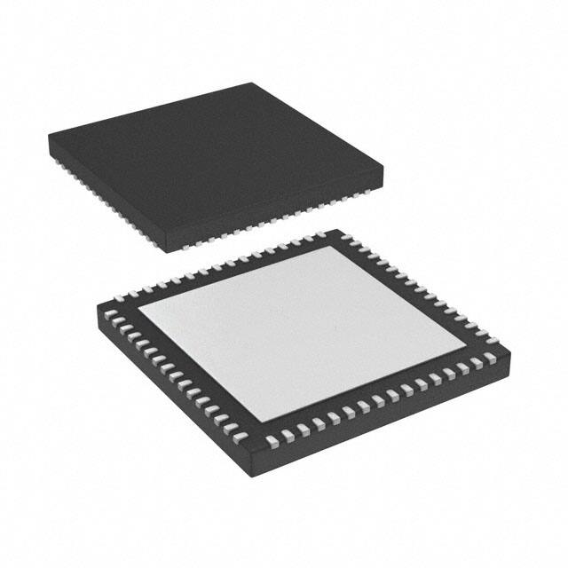
64-QFN Package (9 mm × 9 mm)
DESCRIPTION
ADS62C17 is a dual channel 11-bit, 200 MSPS A/D converter that combines high dynamic performance and low
power consumption in a compact 64 QFN package. This makes it well-suited for multi-carrier, wide band-width
communications applications.
ADS62C17 uses TI-proprietary SNRBoost technology that can be used to overcome SNR limitation due to
quantization noise for bandwidths less than Nyquist (Fs/2). It includes several useful and commonly used digital
functions such as ADC offset correction, gain (0 to 6 dB in steps of 0.5 dB) and gain tuning (in fine steps of 0.001
dB).
The gain option can be used to improve SFDR performance at lower full-scale input ranges. Using the gain
tuning capability, each channel’s gain can be set independently to improve channel-to-channel gain matching.
The device also includes a dc offset correction loop that can be used to cancel the ADC offset.
Both DDR LVDS (Double Data Rate) and parallel CMOS digital output interfaces are available. It includes
internal references while the traditional reference pins and associated decoupling capacitors have been
eliminated. Nevertheless, the device can also be driven with an external reference.
The device is specified over the industrial temperature range (–40°C to 85°C).
1
Please be aware that an important notice concerning availability, standard warranty, and use in critical applications of Texas
Instruments semiconductor products and disclaimers thereto appears at the end of this data sheet.
PRODUCTION DATA information is current as of publication date.
Products conform to specifications per the terms of the Texas
Instruments standard warranty. Production processing does not
necessarily include testing of all parameters.
Copyright © 2009, Texas Instruments Incorporated
�ADS62C17
SLAS631A – APRIL 2009 – REVISED JULY 2009 ............................................................................................................................................................. www.ti.com
DRGND
DRVDD
AGND
AVDD
These devices have limited built-in ESD protection. The leads should be shorted together or the device placed in conductive foam
during storage or handling to prevent electrostatic damage to the MOS gates.
LVDS
INTERFACE
DA0P/M
Digital
Processing
Block
Sample
&
Hold
INA_P
INA_M
14 bit
ADC
DA2P/M
DA4P/M
SNRBoost
11 bit
DDR
Serializer
DA6P/M
DA8P/M
Channel A
DA10P/M
CLKP
CLKM
OUTPUT
CLOCK
BUFFER
CLOCKGEN
CLKOUTP/M
DB0P/M
INB_P
Digital
Processing
Block
Sample
&
Hold
INB_M
14 bit
ADC
DB2P/M
DB4P/M
SNRBoost
11 bit
DDR
Serializer
DB6P/M
DB8P/M
Channel B
DB10P/M
VCM
REFERENCE
CONTROL
INTERFACE
SDOUT
RESET
SCLK
SEN
SDATA
CTRL1
CTRL2
CTRL3
ADS62C17
Figure 1. ADS62C17 Block Diagram
PACKAGE/ORDERING INFORMATION
2
PRODUCT
PACKAGELEAD
PACKAGE
DESIGNATOR
SPECIFIED
TEMPERATURE RANGE
PACKAGE MARKING
ORDERING NUMBER
TRANSPORT
MEDIA,
QUANTITY
ADS62C17
QFN-64
RGC
–40°C to 85°C
AZ62C17
ADS62C17IRGCR
ADS62C17IRGCT
Tape and Reel
Submit Documentation Feedback
Copyright © 2009, Texas Instruments Incorporated
Product Folder Link(s): ADS62C17
�ADS62C17
www.ti.com ............................................................................................................................................................. SLAS631A – APRIL 2009 – REVISED JULY 2009
THERMAL CHARACTERISTICS (1)
over operating free-air temperature range (unless otherwise noted)
PARAMETER
RθJA (2)
RθJT
(1)
(2)
(3)
(3)
TEST CONDITIONS
TYP
Soldered thermal pad, no airflow
22
Soldered thermal pad, 200 LFM
15
Bottom of package (thermal pad)
0.57
UNIT
° C/W
With a JEDEC standard high K board and 5x5 via array. See Exposed Pad in the Application Information.
RθJA is the thermal resistance from the junction to ambient.
RθJT is the thermal resistance from the junction to the thermal pads.
ABSOLUTE MAXIMUM RATINGS (1)
VALUE
Supply voltage range AVDD
-0.3 to 3.9
Supply voltage range DRVDD
–0.3 to 2.2
Voltage between AGND and DRGND
–0.3 to 0.3
Voltage between AVDD to DRVDD (when AVDD leads DRVDD)
0 to 3.3
Voltage between DRVDD to AVDD (when DRVDD leads AVDD)
–1.5 to 1.8
Voltage applied to external pin, VCM (in external refersnce mode)
Voltage applied to analog input pins – INP_A, INM_A, INP_B, INM_B
Voltage applied to input pins – CLKP, CLKM (2), RESET, SCLK, SDATA, SEN, CTRL1,
CTRL2, CTRL3
UNIT
V
V
–0.3 to 2.0
–0.3V to minimum
(3.6, AVDD + 0.3V)
V
–0.3V to ADD + 0.3V
TA
Operating free-air temperature range
–40 to 85
°C
TJ
Operating junction temperature range
125
°C
Tstg
Storage temperature range
ESD, human body model
(1)
(2)
–54 to 150
°C
2
kV
Stresses beyond those listed under “absolute maximum ratings” may cause permanent damage to the device. These are stress ratings
only and functional operation of the device at these or any other conditions beyond those indicated under “recommended operating
conditions” is not implied. Exposure to absolute maximum rated conditions for extended periods may affect device reliability.
When AVDD is turned off, it is recommended to switch off the input clock (or ensure the voltage on CLKP, CLKM is < |0.3V|. This
prevents the ESD protection diodes at the clock input pins from turning on.
Submit Documentation Feedback
Copyright © 2009, Texas Instruments Incorporated
Product Folder Link(s): ADS62C17
3
�ADS62C17
SLAS631A – APRIL 2009 – REVISED JULY 2009 ............................................................................................................................................................. www.ti.com
RECOMMENDED OPERATING CONDITIONS (1)
MIN
TYP
MAX
UNIT
SUPPLIES
AVDD
Analog supply voltage
3.15
3.3
3.8
V
DRVDD
Digital supply voltage
1.7
1.8
1.9
V
ANALOG INPUTS
Differential input voltage range
2
Input common-mode voltage
VPP
1.5 ± 0.1
Voltage applied on CM in external reference mode
V
1.5 ± 0.05
V
Maximum analog input frequency with 2V pp input amplitude
(1)
500
MHz
Maximum analog input frequency with 1V pp input amplitude
(1)
800
MHz
CLOCK INPUT
Input clock sample rate
1
200 MSPS
Input Clock amplitude differential (VCLKP– VCLKM)
Sine wave, ac-coupled
3.0
VPP
LVPECL, ac-coupled
1.6
VPP
LVDS, ac-coupled
0.7
VPP
LVCMOS, single-ended, ac-coupled
3.3
V
Input clock duty cycle
0.2
40%
50%
60%
DIGITAL OUTPUTS
CL
Maximum external load capacitance from each output pin to DRGND
RL
Differential external load resistance between the LVDS output (LVDS interface)
TA
Operating free-air temperature
(1)
4
–40
5
pF
100
Ω
85
°C
See Theory of Operation in the application section.
Submit Documentation Feedback
Copyright © 2009, Texas Instruments Incorporated
Product Folder Link(s): ADS62C17
�ADS62C17
www.ti.com ............................................................................................................................................................. SLAS631A – APRIL 2009 – REVISED JULY 2009
ELECTRICAL CHARACTERISTICS (1)
Typical values are at 25°C, AVDD = 3.3V, DRVDD = 1.8V, sampling frequency = 200 MSPS, 50% clock duty cycle, –1dBFS
differential analog input, internal reference mode, LVDS and CMOS interfaces unless otherwise noted.
Min and max values are across the full temperature range TMIN = –40°C to TMAX = 85°C, AVDD = 3.3V, DRVDD = 1.8V
PARAMETER
TEST CONDITIONS
MIN
TYP
Resolution
MAX
UNIT
11
bits
ANALOG INPUTS
Differential input voltage range
2.0
VPP
Differential input resistance (at dc)
See Figure 44
>1
MΩ
Differential input capacitance
See Figure 45
3.5
pF
Analog input bandwidth
700
MHz
Analog input common mode current (per channel)
3.6
µA/MSPS
VCM common mode voltage output
1.5
V
VCM output current capability
±4
mA
262
mA
120
mA
87
mA
POWER SUPPLY
IAVDD
Analog supply current
IDRVDD
Output buffer supply current LVDS interface
With 100 Ω external
termination
IDRVDD
Output buffer supply current CMOS interface
No external load
capacitance
Analog power
865
1025
mW
Digital power LVDS interface
216
306
mW
45
75
mW
Global power down
No missing codes
Assured
DC ACCURACY
DNL
Differential Non-Linearity
Fin = 170 MHz
-0.6
±0.2
0.6
LSB
INL
Integral Non-Linearity
Fin = 170 MHz
-2.5
±0.75
2.5
LSB
-20
±2
20
mV
Offset Error
Offset error temperature coefficient
Offset error variation with supply
0.02
mV/C
0.5
mV/V
There are two sources of gain error – internal reference inaccuracy and channel gain error
Gain error due to internal reference inaccuracy alone
-1
±0.2
1
Gain error of channel alone (2)
-1
+0.2
1
Channel gain error temperature coefficient
Gain matching
(1)
(2)
(3)
(3)
-2
Difference in gain errors
between two channels
across two devices
-4
% FS
Δ%/°C
0.002
Difference in gain errors
between two channels
within the same device
% FS
2
% FS
4
In CMOS interface, the DRVDD current scales with the sampling frequency and the load capacitance on output pins.
This is specified by design and characterization; it is not tested in production.
For two channels within the same device, only the channel gain error matters, as the reference is common for both channels.
Submit Documentation Feedback
Copyright © 2009, Texas Instruments Incorporated
Product Folder Link(s): ADS62C17
5
�ADS62C17
SLAS631A – APRIL 2009 – REVISED JULY 2009 ............................................................................................................................................................. www.ti.com
ELECTRICAL CHARACTERISTICS
Typical values are at 25°C, AVDD = 3.3V, DRVDD = 1.8V, sampling frequency = 200 MSPS, 50% clock duty cycle, –1dBFS
differential analog input, internal reference mode, SNRBoost disabled, LVDS and CMOS interfaces unless otherwise noted.
Min and max values are across the full temperature range TMIN = –40°C to TMAX = 85°C, AVDD = 3.3V, DRVDD = 1.8V
PARAMETER
SNR
Signal to noise ratio
LVDS
TEST CONDITIONS
MIN
TYP MAX
Fin = 20 MHz
67
Fin = 70 MHz
66.8
Fin = 170 MHz
0 dB gain
64.5
6 dB gain
UNIT
dBFS
66.3
64.4
Table 1. SNR Enhancement With SNRBoost Enabled
SNRBoost bath-tub centered at Fsx0.25, –1 dBFS input applied at Fin = 125MHz, Sampling frequency = 200MSPS
SNR Within Specified bandwidth, dBFS
Bandwidth, MHz
(1)
6
With SNRBoost Enabled (1)
In Default Mode (SNRBoost Disabled)
MIN
TYP
5
78.8
79.6
10
75.8
15
74
20
MAX
MIN
TYP
83
85.6
76.6
80
82.6
74.9
78.2
80.9
72.7
73.6
77
79.6
30
71
71.9
74.4
76.4
40
69.8
70.6
72.7
74.5
MAX
Using recommended SNRBoost coefficients. See note on SNRBoost in application section.
Submit Documentation Feedback
Copyright © 2009, Texas Instruments Incorporated
Product Folder Link(s): ADS62C17
�ADS62C17
www.ti.com ............................................................................................................................................................. SLAS631A – APRIL 2009 – REVISED JULY 2009
ELECTRICAL CHARACTERISTICS
Typical values are at 25°C, AVDD = 3.3V, DRVDD = 1.8V, sampling frequency = 200 MSPS, 50% clock duty cycle, –1dBFS
differential analog input, internal reference mode, SNRBoost disabled, 0dB gain, LVDS and CMOS interfaces unless
otherwise noted.
Min and max values are across the full temperature range TMIN = –40°C to TMAX = 85°C, AVDD = 3.3V, DRVDD = 1.8V
PARAMETER
TEST CONDITIONS
MIN
Fin= 20 MHz
SINAD
Signal to Noise and Distortion Ratio
66.6
0 dB gain
63.5
6 dB gain
THD
Total Harmonic Distortion
83
0 dB gain
73
6 dB gain
83
Fin = 70 MHz
81
0 dB gain
71.5
6 dB gain
90
0 dB gain
73
6 dB gain
dBc
83
dBc
92
85
Fin = 70 MHz
83
0 dB gain
73
6 dB gain
78
dBc
81
Fin= 20 MHz
Worst Spur
Other than second, third harmonics
75.5
94
Fin= 20 MHz
Fin = 170 MHz
dBc
79
Fin = 70 MHz
Fin = 170 MHz
dBFS
81
Fin= 20 MHz
HD3
Third Harmonic Distortion
78
Fin= 20 MHz
Fin = 170 MHz
HD2
Second Harmonic Distortion
65.7
85
Fin = 70 MHz
Fin = 170 MHz
UNIT
64.2
Fin= 20 MHz
SFDR
Spurious Free Dynamic Range
MAX
66.9
Fin = 70 MHz
Fin = 170 MHz
TYP
94
Fin = 70 MHz
92
Fin = 170 MHz
80
IMD
2-Tone Inter-modulation Distortion
F1 = 185 MHz, F2 = 190 MHz, Each tone at –7 dBFS
Input Overload recovery
Recovery to within 1% (of final value) for 6-dB overload with
sine wave input at Fclk/4
Cross-talk
PSRR
AC Power Supply Rejection Ratio
dBc
90
87
dBFS
1
clock
cycles
Up to 200 MHz cross-talk frequency
90
dB
For 100 mV pp signal on AVDD supply
25
dB
Submit Documentation Feedback
Copyright © 2009, Texas Instruments Incorporated
Product Folder Link(s): ADS62C17
7
�ADS62C17
SLAS631A – APRIL 2009 – REVISED JULY 2009 ............................................................................................................................................................. www.ti.com
DIGITAL CHARACTERISTICS — ADS62C17
The DC specifications refer to the condition where the digital outputs are not switching, but are permanently at a valid logic
level 0 or 1. AVDD = 3.3V, DRVDD = 1.8V
PARAMETER
TEST CONDITIONS
DIGITAL INPUTS – CTRL1, CTRL2, CTRL3, RESET, SCLK, SDATA, SEN
High-level input voltage
MIN
High-level input current
Low-level input current
MAX
1.3
All digital inputs support 1.8 V and 3.3 V CMOS
logic levels.
Low-level input voltage
TYP
UNIT
(1)
0.4
SDATA, SCLK (2)
VHIGH = 3.3 V
16
SEN (3)
VHIGH = 3.3 V
10
SDATA, SCLK
VLOW = 0 V
0
SEN
VLOW = 0 V
–20
Input capacitance
V
µA
µA
4
pF
DRVDD – DRVDD
0.1
V
DIGITAL OUTPUTS – CMOS INTERFACE (DA0-DA10, DB0-DB10, CLKOUT, SDOUT)
High-level output voltage
Low-level output voltage
Ioh = 1mA
Iol = 1mA
0
Output capacitance (internal to device)
0.1
2
V
pF
DIGITAL OUTPUTS – LVDS INTERFACE (DA0P/M TO DA10P/M, DB0P/M TO DB10P/M, CLKOUTP/M)
VODH, High-level output differential voltage
With external 100 Ω termination
+275
+350
+425
mV
VODL, Low-level output differential voltage
With external 100 Ω termination.
–425
–350
–275
mV
1.0
1.15
1.40
VOCM, Output common-mode voltage
Capacitance inside the device from each output
to ground
Output Capacitance
(1)
(2)
(3)
2
V
pF
SCLK, SDATA, SEN function as digital input pins in serial configuration mode.
SDATA, SCLK have internal 200 kΩ pull-down resistor
SEN has internal 100 kΩ pull-up resistor to AVDD.
DAnP / DBnP
Logic 0
VODL = -350 mV*
Logic 1
VODH = +350 mV*
DAnM / DBnM
VOCM
GND
GND
* With external 100 W termination
Figure 2. LVDS Output Voltage Levels
8
Submit Documentation Feedback
Copyright © 2009, Texas Instruments Incorporated
Product Folder Link(s): ADS62C17
�ADS62C17
www.ti.com ............................................................................................................................................................. SLAS631A – APRIL 2009 – REVISED JULY 2009
TIMING CHARACTERISTICS — LVDS AND CMOS MODES (1)
Typical values are at 25°C, AVDD = 3.3V, DRVDD = 1.8V, sampling frequency = 200 MSPS, sine wave input clock, CLOAD =
5pF (2), RLOAD = 100 Ω (3), no internal termination, LOW SPEED mode disabled, unless otherwise noted.
Min and max values are across the full temperature range TMIN = –40°C to TMAX = 85°C, AVDD = 3.3V, DRVDD = 1.7V to
1.9V.
PARAMETER
ta
TEST CONDITIONS
Aperture delay
Aperture delay matching
tj
MIN
TYP
MAX
0.7
1.2
1.7
between two channels of the same device
Aperture jitter
Wake-up time
ADC Latency (4)
UNIT
ns
±50
ps
145
fs rms
Time to valid data after coming out of STANDBY mode
1
3
Time to valid data after coming out of global powerdown
20
50
Time to valid data after stopping and restarting the input clock
10
Default, after reset
22
µs
Clock
cycles
DDR LVDS MODE (5)
Data setup time (6)
tsu
(7)
th
Data hold time
tPDI
Clock propagation delay
tdelay
Data valid (7) to zero-crossing of CLKOUTP
0.8
1.15
ns
Zero-crossing of CLKOUTP to data becoming invalid (7)
0.8
1.15
ns
Input clock falling edge cross-over to output clock rising edge
cross-over
100 MSPS ≤ Sampling frequency ≤ 200 MSPS
Ts = 1/Sampling frequency
tPDI = 0.69×Ts + tdelay
4.2
5.7
7.2
ns
tdelay skew
Difference in tdelay between two devices operating at same
temperature & SVDD supply voltage.
±500
LVDS bit clock duty cycle
Duty cycle of differential clock, (CLKOUTP-CLKOUTM)
100 MSPS ≤ Sampling frequency ≤ 200 MSPS
52%
tRISE, tFALL
Data rise time, Data fall time
Rise time measured from –100 mV to +100 mV
Fall time measured from +100 mV to –100 mV
1MSPS ≤ Sampling frequency ≤ 200 MSPS
0.14
ns
tCLKRISE,
tCLKFALL
Output clock rise time,
Output clock fall time
Rise time measured from –100 mV to +100 mV
Fall time measured from +100 mV to –100 mV
1 MSPS ≤ Sampling frequency ≤ 200 MSPS
0.14
ns
tOE
Output buffer enable to data delay
Time to valid data after output buffer becomes active
100
ns
ps
PARALLEL CMOS MODE at Fs=200 MSPS (8)
tSTART
Input clock to data delay
Input clock falling edge cross-over to start of data valid (7)
tDV
Data valid time
Time interval of valid data (7)
1.7
tPDI
Clock propagation delay
Input clock falling edge cross-over to output clock rising edge
cross-over
100 MSPS ≤ Sampling frequency ≤ 150 MSPS
Ts = 1/Sampling frequency
tPDI = 0.28×Ts + tdelay
tdelay
2.5
5.5
2.7
7.5
ns
ns
8.5
ns
Output clock duty cycle
Duty cycle of output clock, CLKOUT
100 MSPS ≤ Sampling frequency ≤ 150 MSPS
43
tRISE, tFALL
Data rise time, Data fall time
Rise time measured from 20% to 80% of DRVDD
Fall time measured from 80% to 20% of DRVDD
1 ≤ Sampling frequency ≤ 200 MSPS
1.2
ns
tCLKRISE,
tCLKFALL
Output clock rise time,
Output clock fall time
Rise time measured from 20% to 80% of DRVDD
Fall time measured from 80% to 20% of DRVDD
1 ≤ Sampling frequency ≤ 150 MSPS
0.8
ns
tOE
Output buffer enable (OE) to data
delay
Time to valid data after output buffer becomes active
100
ns
(1)
(2)
(3)
(4)
(5)
(6)
(7)
(8)
Timing parameters are ensured by design and characterization and not tested in production.
CLOAD is the effective external single-ended load capacitance between each output pin and ground
RLOAD is the differential load resistance between the LVDS output pair.
At higher frequencies, tPDI is greater than one clock period and overall latency = ADC latency + 1.
Measurements are done with a transmission line of 100Ω characteristic impedance between the device and the load.
Setup and hold time specifications take into account the effect of jitter on the output data and clock.
Data valid refers to LOGIC HIGH of +100.0mV and LOGIC LOW of -100.0mV.
Data valid refers to LOGIC HIGH of 1.26V and LOGIC LOW of 0.54V.
For Fs> 150 MSPS, it is recommended to use external clock for data capture and NOT the device output clock signal (CLKOUT).
Submit Documentation Feedback
Copyright © 2009, Texas Instruments Incorporated
Product Folder Link(s): ADS62C17
9
�ADS62C17
SLAS631A – APRIL 2009 – REVISED JULY 2009 ............................................................................................................................................................. www.ti.com
Table 2. LVDS Timings at Lower Sampling Frequencies
Sampling Frequency, MSPS
Setup Time, ns
Hold Time, ns
MIN
TYP
185
0.9
1.25
MAX
MIN
TYP
0.85
1.25
150
1.15
1.6
1.1
1.5
125
1.6
2
1.45
1.85
100 MSPS.
1 Enable LOW SPEED mode for sampling frequencies about 300 MHz), SFDR is determined largely by the device’s sampling circuit
non-linearity. At low input amplitudes, the quantizer non-linearity usually limits performance.
Submit Documentation Feedback
Copyright © 2009, Texas Instruments Incorporated
Product Folder Link(s): ADS62C17
43
�ADS62C17
SLAS631A – APRIL 2009 – REVISED JULY 2009 ............................................................................................................................................................. www.ti.com
Glitches are caused by the opening & closing of the sampling switches. The driving circuit should present a low
source impedance to absorb these glitches. Otherwise, this could limit performance, mainly at low input
frequencies (up to about 200 MHz). It is also necessary to present low impedance (< 50 Ω) for the common
mode switching currents. This can be achieved by using two resistors from each input terminated to the common
mode voltage (VCM).
The device includes an internal R-C filter from each input to ground. The purpose of this filter is to absorb the
sampling glitches inside the device itself. The cut-off frequency of the R-C filter involves a trade-off.
A lower cut-off frequency (larger C) absorbs glitches better, but it reduces the input bandwidth. On the other
hand, with a higher cut-off frequency (smaller C), bandwidth support is maximized. But now, the sampling
glitches need to be supplied by the external drive circuit. This has limitations due to the presence of the package
bond-wire inductance.
In ADS62C17, the R-C component values have been optimized while supporting high input bandwidth (up to 700
MHz). However, in applications with input frequencies up to 200-300MHz, the filtering of the glitches can be
improved further using an external R-C-R filter (as shown in Figure 46 and Figure 47).
In addition to the above, the drive circuit may have to be designed to provide a low insertion loss over the
desired frequency range and matched impedance to the source. While doing this, the ADC input impedance
must be considered. Figure 44 and Figure 45 show the impedance (Zin = Rin || Cin) looking into the ADC input
pins.
100
Resistance - kW
10
1
0.10
0.01
0
100
200
300
400
500
600
f - Frequency - MHz
700
800
900
1000
Figure 44. ADC Analog Input Resistance (Rin) Across Frequency
44
Submit Documentation Feedback
Copyright © 2009, Texas Instruments Incorporated
Product Folder Link(s): ADS62C17
�ADS62C17
www.ti.com ............................................................................................................................................................. SLAS631A – APRIL 2009 – REVISED JULY 2009
4.5
4
Capacitance - pF
3.5
3
2.5
2
1.5
1
0
100
200
300
400
500
600
700
800
900
1000
f - Frequency - MHz
Figure 45. ADC Analog Input Capacitance (Cin) Across Frequency
Driving Circuit
Two example driving circuit configurations are shown in Figure 46 and Figure 47 – one optimized for low
bandwidth (low input frequencies) and the other one for high bandwidth to support higher input frequencies.
In Figure 46, an external R-C-R filter using 22pF has been used. Together with the series inductor (39nH), this
combination forms a filter and absorbs the sampling glitches. Due to the large capacitor (22pF) in the R-C-R and
the 15Ω resistors in series with each input pin, the drive circuit has low bandwidth and supports low input
frequencies ( 300MHz). For example, a transmission line transformer such as ADTL2-18 can be used
(Figure 48).
Note that both the drive circuits have been terminated by 50 ohms near the ADC side. The termination is
accomplished by a 25 ohms resistor from each input to the 1.5V common-mode (VCM) from the device. This
allows the analog inputs to be biased around the required common-mode voltage.
Submit Documentation Feedback
Copyright © 2009, Texas Instruments Incorporated
Product Folder Link(s): ADS62C17
45
�ADS62C17
SLAS631A – APRIL 2009 – REVISED JULY 2009 ............................................................................................................................................................. www.ti.com
39 nH
0.1 mF
15 W
0.1 mF
INP
50 W
0.1uF
50 W
25 W
22 pF
25 W
50 W
50 W
1:1
INM
1:1
15 W
0.1 mF
39 nH
VCM
Figure 46. Drive Circuit With Low Bandwidth (for low input frequencies)
The mismatch in the transformer parasitic capacitance (between the windings) results in degraded even-order
harmonic performance. Connecting two identical RF transformers back to back helps minimize this mismatch and
good performance is obtained for high frequency input signals. An additional termination resistor pair may be
required between the two transformers as shown in the figures. The center point of this termination is connected
to ground to improve the balance between the P and M sides. The values of the terminations between the
transformers and on the secondary side have to be chosen to get an effective 50Ω (in the case of 50Ω source
impedance).
0.1 mF
5W
0.1 mF
INP
0.1 mF
50 W
25 W
3.3 pF
25 W
50 W
INM
1:1
1:1
5W
0.1 mF
VCM
Figure 47. Drive Circuit With High Bandwidth (for high input frequencies)
0.1μF
INP
0.1μF
25 Ω
25 Ω
T1
T2
INM
0.1μF
VCM
Figure 48. Drive circuit with very high bandwidth (> 300 MHz)
46
Submit Documentation Feedback
Copyright © 2009, Texas Instruments Incorporated
Product Folder Link(s): ADS62C17
�ADS62C17
www.ti.com ............................................................................................................................................................. SLAS631A – APRIL 2009 – REVISED JULY 2009
All these examples show 1:1 transformers being used with a 50 ohms source. As explained in the "Drive Circuit
Requirements", this helps to present a low source impedance to absorb the sampling glitches. With a 1:4
transformer, the source impedance will be 200 ohms. The higher impedance can lead to degradation in
performance, compared to the case with 1:1 transformers. For applications where only a band of frequencies are
used, the drive circuit can be tuned to present a low impedance for the sampling glitches. Figure 49 shows an
example with 1:4 transformer, tuned for a band around 150MHz.
5Ω
INP
25 Ω
100 Ω
0.1μF
Differential
input signal
72 nH
15 pF
100 Ω
25 Ω
INM
5Ω
1:4
VCM
Figure 49. Drive circuit with 1:4 transformer
Input common-mode
To ensure a low-noise common-mode reference, the VCM pin is filtered with a 0.1µF low-inductance capacitor
connected to ground. The VCM pin is designed to directly drive the ADC inputs. The input stage of the ADC
sinks a common-mode current in the order of 3.6 µA / MSPS (about 720 µA at 200 MSPS).
REFERENCE
ADS62C17 has built-in internal references REFP and REFM, requiring no external components. Design schemes
are used to linearize the converter load seen by the references; this and the on-chip integration of the requisite
reference capacitors eliminates the need for external decoupling. The full-scale input range of the converter can
be controlled in the external reference mode as explained below. The internal or external reference modes can
be selected by programming the serial interface register bit .
INTREF
+
_
VCM
INTERNAL
REFERENCE
EXTREF
_
+
REFM
REFP
Figure 50. Reference Section
Internal reference
When the device is in internal reference mode, the REFP and REFM voltages are generated internally.
Common-mode voltage (1.5V nominal) is output on VCM pin, which can be used to externally bias the analog
input pins
Submit Documentation Feedback
Copyright © 2009, Texas Instruments Incorporated
Product Folder Link(s): ADS62C17
47
�ADS62C17
SLAS631A – APRIL 2009 – REVISED JULY 2009 ............................................................................................................................................................. www.ti.com
External reference
When the device is in external reference mode, the VCM acts as a reference input pin. The voltage forced on the
VCM pin is buffered and gained by 1.33 internally, generating the REFP and REFM voltages. The differential
input voltage corresponding to full-scale is given by the following:
Full-scale differential input pp = (Voltage forced on VCM) × 1.33
In this mode, the 1.5V common-mode voltage to bias the input pins has to be generated externally.
SNR ENHANCEMENT USING SNRBOOST
SNRBoost technology makes it possible to overcome SNR limitations due to quantization noise. With SNRBoost,
enhanced SNR can be obtained for any bandwidth (less than Nyquist or Fs/2, see Table 1). The SNR
improvement is achieved without affecting the default harmonic performance. SNRBoost is disabled after reset; it
can be enabled using register bit or using the control pins CTRL1, 2, 3.
(While using the register bits to control SNRBoost, keep CTRL1, CTRL2, CTRL3 low. To use the CTRL pins as
SNRBoost control, reset the register bits).
When it is enabled, the noise floor in the spectrum acquires a typical bath-tub shape as shown in Figure 51. The
bath-tub is centered around a specific frequency (called center frequency). The center frequency is located
mid-way between two corner frequencies, which are specified by the SNRBoost coefficients (Register bits
and SNRBoost Coeff2>).
Table 9 shows the relation between each coefficient and its corner frequency. By choosing appropriate
coefficients, the bath-tub can be positioned over the frequency range 0 to Fs/2 (Table 10 shows some
examples). By positioning the bath-tub within the desired signal band, SNR improvement can be achieved (see
Table 1). Note that as the bandwidth is increased, the amount of SNR improvement reduces.
0
Fs = 200MSPS
Fin =150 MHz
SNRBoost Coeff1 = 0x0F,
SNRBoost Coeff2 = 0x01,
Amplitude - dB
-20
-40
Center Frequency
= FS x 0.25
-60
-80
-100
-120
-140
0
0.05
0.10
0.15
0.20
0.25
0.30
f - Frequency - MHz
0.35
0.40
0.45
0.50
Figure 51. Specturm with SNRBoost Enabled
Table 9. Setting the Corner Frequency
48
SNRBoost Coefficient Value
Normalized Corner Frequency
(f/fs)
SNRBoost Coefficient value
Normalized Corner Frequency
(f/fs)
7
6
0.420
F
0.230
0.385
E
0.210
5
0.357
D
0.189
4
0.333
C
0.167
3
0.311
B
0.143
2
0.290
A
0.115
1
0.270
9
0.080
0
0.250
8
0.000
Submit Documentation Feedback
Copyright © 2009, Texas Instruments Incorporated
Product Folder Link(s): ADS62C17
�ADS62C17
www.ti.com ............................................................................................................................................................. SLAS631A – APRIL 2009 – REVISED JULY 2009
Table 10. Positioning the Corner Frequency (Some Examples)
SNRBoost Coefficient1,
Normalized Corner
Frequency1
(f/fs)
SNRBoost Coefficient1,
Normalized Corner
Frequency2
(f/fs)
Center Frequency
0
0.250
0
0.250
Fs × 0.25
F
0.230
1
0.270
Fs × 0.25
6
0.385
2
0.290
Fs × 0.3375
D
0.189
B
0.143
Fs × 0.166
9
0.080
7
0.420
Fs × 0.25
Serial register write to enable SNRBoost
Register address = 0x59
SDATA
A7
A6
A1
Register data = 0x01
A0
D7
D6
D1
D0
10 clock cycles after the 16th SCLK
falling edge, the device starts
giving out valid SNRBoost data
SCLK
SEN
clock
cycle 1
clock
cycle 9
clock
cycle 10
CLKM
CLKP
N
Analog
Input
Signal
Output
Data
N+1
N-1
N-26
N-25
Valid SNRBoost
data starts
Figure 52. SNRBoost Active Delay
SNRBoost does not introduce any group delay in the input signal path. The ADC latency increases by four clock
cycle (to 26 clock cycles). When it is enabled using the serial interface, the mode becomes fully active 10 input
clock cycles after the 16th SCLK falling edge. When it is disabled, normal data (without SNRBoost) resumes after
6 clock cycle.
CLOCK INPUT
ADS62C17 clock inputs can be driven differentially (sine, LVPECL or LVDS) or single-ended (LVCMOS), with
little or no difference in performance between them. The common-mode voltage of the clock inputs is set to VCM
using internal 5-kΩ resistors as shown in Figure 53. This allows using transformer-coupled drive circuits for sine
wave clock or ac-coupling for LVPECL, LVDS clock sources (Figure 54 and Figure 55).
Submit Documentation Feedback
Copyright © 2009, Texas Instruments Incorporated
Product Folder Link(s): ADS62C17
49
�ADS62C17
SLAS631A – APRIL 2009 – REVISED JULY 2009 ............................................................................................................................................................. www.ti.com
Clock buffer
Lpkg
~2 nH
20 W
CLKP
Cbond
~1 pF
Ceq
Ceq
5 kW
R
~100 W
VCM
2 pF
5 kW
Lpkg
~ 2 nH
20 W
CLKM
Cbond
~1 pF
R
~100 W
Ceq~ 1 to 3 pF, equivalent input capacitance of clock buffer
Figure 53. Internal Clock Buffer
For best performance, the clock inputs have to be driven differentially, reducing susceptibility to common-mode
noise. For high input frequency sampling, it is recommended to use a clock source with very low jitter. Band-pass
filtering of the clock source can help reduce the effect of jitter. There is no change in performance with a
non-50% duty cycle clock input.
0.1 mF
CLKP
Differential sine-wave
or PECL or LVDS clock input
CLKM
0.1 mF
Figure 54. Differential Clock Driving Circuit
Single-ended CMOS clock can be ac-coupled to the CLKP input, with CLKM tied to 1.5V common-mode voltage.
As shown in Figure 55, CLKM can be tied to VCM pin.
50
Submit Documentation Feedback
Copyright © 2009, Texas Instruments Incorporated
Product Folder Link(s): ADS62C17
�ADS62C17
www.ti.com ............................................................................................................................................................. SLAS631A – APRIL 2009 – REVISED JULY 2009
0.1 mF
CMOS clock input
CLKP
VCM
CLKM
0.1 mF
Figure 55. Single-Ended Clock Driving Circuit
GAIN PROGRAMMABILITY
ADS62C17 includes gain settings that can be used to get improved SFDR performance (compared to 0dB gain).
The gain is programmable from 0dB to 6dB (in 0.5 dB steps). For each gain setting, the analog input full-scale
range scales proportionally, as shown in Table 11.
The SFDR improvement is achieved at the expense of SNR; for each 1dB gain step, the SNR degrades about
1dB. The SNR degradation is less at high input frequencies. As a result, the gain is very useful at high input
frequencies as the SFDR improvement is significant with marginal degradation in SNR.
So, the gain can be used to trade-off between SFDR and SNR. Note that the default gain after reset is 0 dB.
Table 11. Full-Scale Range Across Gains
Gain, dB
Full-Scale, Vpp
0
2V
1
1.78
2
1.59
3
1.42
4
1.26
5
1.12
6
1.00
OFFSET CORRECTION
ADS62C17 has an internal offset correction algorithm that estimates and corrects dc offset up to +/-10mV. The
correction can be enabled using the serial register bit . Once enabled, the
algorithm estimates the channel offset and applies the correction every clock cycle. The time constant of the
correction loop is a function of the sampling clock frequency. The time constant can be controlled using register
bits as described in Table 12.
After the offset is estimated, the correction can be frozen by setting = 0.
Once frozen, the last estimated value is used for offset correction every clock cycle. The correction does not
affect the phase of the signal. Note that offset correction is disabled by default after reset.
Figure 56 shows the time response of the offset correction algorithm, after it is enabled.
Submit Documentation Feedback
Copyright © 2009, Texas Instruments Incorporated
Product Folder Link(s): ADS62C17
51
�ADS62C17
SLAS631A – APRIL 2009 – REVISED JULY 2009 ............................................................................................................................................................. www.ti.com
Table 12. Time Constant of Offset Correction Algorithm
(1)
D3-D0
Time Constant (TCCLK),
Number of Clock Cycles
Time Constant, sec
(=TCCLK x 1/Fs) (1)
0000
256 k
1.2 ms
0001
512 k
2.5 ms
0010
1M
5 ms
0011
2M
10 ms
0100
4M
20 ms
0101
8M
40 ms
0110
16 M
80 ms
0111
32 M
0.16 s
1000
64 M
0.32 s
1001
128 M
0.64 s
1010
256 M
1.28 s
1011
512 M
2.5 s
1100
RESERVED
1101
RESERVED
1110
RESERVED
1111
RESERVED
Sampling frequency, Fs = 200 MSPS
1026
Offset correction
enabled
1025
Output Codesm - LSB
1024
Output data with
offset corrected
Offset correction
disabled
1023
1022
1021
1020
1019
1018
-2
Output data with
4 LSB offset
0
2
4
6
8
10
12
14
16
18
20
Time - ms
Figure 56. Time Response of Offset Correction
POWER DOWN
ADS62C17 has three power down modes – power down global, individual channel standby and individual
channel output buffer disable. These can be set using either the serial register bits or using the control pins
CTRL1 to CTRL3.
52
Submit Documentation Feedback
Copyright © 2009, Texas Instruments Incorporated
Product Folder Link(s): ADS62C17
�ADS62C17
www.ti.com ............................................................................................................................................................. SLAS631A – APRIL 2009 – REVISED JULY 2009
Table 13. Power Down Controls
POWER DOWN MODES
CONFIGURE USING
SERIAL INTERFACE
PARALLEL CONTROL
PINS
low
WAKE-UP
TIME
Normal operation
=0000
low
low
–
Output buffer disabled for channel B
=1001
–
Output buffer disabled for channel A
=1010
The pins do not
support output buffer
disable
Output buffer disabled for channel A and B
=1011
Global power down
=1100
high
Channel B standby
=1101
Channel A standby
=1110
Multiplexed (MUX) mode – Output data of channel A
and B is multiplexed & available on DA10 to DA0
pins.
=1111
–
Fast (100 ns)
low
low
Slow (20 µs)
high
low
high
Fast (1 µs)
high
high
low
Fast (1 µs)
high
high
high
–
Power Down Global
In this mode, the entire chip including both the A/D converters, internal reference and the output buffers are
powered down resulting in reduced total power dissipation of about 45mW. The output buffers are in high
impedance state. The wake-up time from the global power down to data becoming valid in normal mode is
typically 20 µs.
Channel Power Down (individual or both channels)
Here, each channel’s A/D converter can be powered down. The internal references are active, resulting in quick
wake-up time of 1 µs. The total power dissipation in standby is about 450 mW.
Output Buffer Disable (individual or both channels)
Each channel’s output buffer can be disabled and put in high impedance state – wakeup time from this mode is
fast, about 100 ns.
Input Clock Stop
In addition to the above, the converter enters a low-power mode when the input clock frequency falls below
1MSPS. The power dissipation is about 275 mW.
POWER SUPPLY SEQUENCE
During power-up, the AVDD and DRVDD supplies can come up in any sequence. The two supplies are
separated in the device.
DIGITAL OUTPUT INTERFACE
ADS62C17 provides 11-bit data and an output clock synchronized with the data.
Two output interface options are available – Double Data Rate (DDR) LVDS and parallel CMOS. They can be
selected using the serial interface register bit or using DFS pin in parallel configuration mode.
DDR LVDS Interface
In this mode, the data bits and clock are output using LVDS (Low Voltage Differential Signal) levels. Two data
bits are multiplexed and output on each LVDS differential pair.
Submit Documentation Feedback
Copyright © 2009, Texas Instruments Incorporated
Product Folder Link(s): ADS62C17
53
�ADS62C17
SLAS631A – APRIL 2009 – REVISED JULY 2009 ............................................................................................................................................................. www.ti.com
CLKOUTP
Output Clock
CLKOUTM
DB0_P
DB0_M
Data bit D0
DB2_P
DB2_M
Data bits D1, D2
DB4_P
DB4_M
11 bit ADC data
Channel B
DB6_P
DB6_M
Data bits D3, D4
Data bits D5, D6
DB8_P
DB8_M
Data bits D7, D8
DB10_P
DB10_M
ADS62C17
Data bits D9, D10
LVDS Buffers
Figure 57. DDR LVDS Outputs
Even data bits D0, D2, D4… are output at the falling edge of CLKOUTP and the odd data bits D1, D3, D5… are
output at the rising edge of CLKOUTP. Both the rising and falling edges of CLKOUTP have to be used to capture
all the data bits (Figure 58).
54
Submit Documentation Feedback
Copyright © 2009, Texas Instruments Incorporated
Product Folder Link(s): ADS62C17
�ADS62C17
www.ti.com ............................................................................................................................................................. SLAS631A – APRIL 2009 – REVISED JULY 2009
CLKOUTM
CLKOUTP
DA0, DB0
DA2, DB2
DA4,DB4
0
D0
0
D0
D1
D2
D1
D2
D3
D4
D3
D4
D5
D6
D5
D6
D7
D8
D7
D8
D9
D10
D9
D10
DA6,DB6
DA8,DB8
DA10,DB10
SAMPLE N
SAMPLE N+1
Figure 58. DDR LVDS Interface
LVDS Buffer
The equivalent circuit of each LVDS output buffer is shown in Figure 59. The buffer is designed to present an
output impedance of 100Ω (Rout). The differential outputs can be terminated at the receive end by a 100Ω
termination.
The buffer output impedance behaves like a source-side series termination. By absorbing reflections from the
receiver end, it helps to improve signal integrity. Note that this internal termination cannot be disabled and its
value cannot be changed.
Submit Documentation Feedback
Copyright © 2009, Texas Instruments Incorporated
Product Folder Link(s): ADS62C17
55
�ADS62C17
SLAS631A – APRIL 2009 – REVISED JULY 2009 ............................................................................................................................................................. www.ti.com
Low
- 0.35 V
High
1.2 V
High
+ 0.35 V
Low
ADS62C18
OUTP
Rout
OUTM
Switch impedance is
nominally 50 W (+/- 10%)
When the “High” switches are closed , OUTP = 1.375 V, OUTM = 1.025 V
When the “Low” switches are closed , OUTP = 1.025 V, OUTM = 1.375 V
When the “High” (or “Low”) switches are closed, Rout = 100 W
Figure 59. LVDS Buffer Equivalent Circuit
Parallel CMOS Interface
In the CMOS mode, each data bit is output on separate pin as CMOS voltage level, every clock cycle. The rising
edge of the output clock CLKOUT can be used to latch data in the receiver (for sampling frequencies up to
150 MSPS).
Up to 150MSPS, the setup and hold timings of the output data with respect to CLKOUT are specified. It is
recommended to minimize the load capacitance seen by data and clock output pins by using short traces to the
receiver. Also, match the output data and clock traces to minimize the skew between them.
For sampling frequencies above 150 MSPS, it is recommended to use an external clock to capture data. The
delay from input clock to output data and the data valid times are specified for the higher sampling frequencies.
These timings can be used to delay the input clock appropriately and use it to capture the data.
56
Submit Documentation Feedback
Copyright © 2009, Texas Instruments Incorporated
Product Folder Link(s): ADS62C17
�ADS62C17
www.ti.com ............................................................................................................................................................. SLAS631A – APRIL 2009 – REVISED JULY 2009
Pins
DB0
DB1
DB2
DB8
11 bit ADC data
Channel B
DB9
DB10
SDOUT
CLKOUT
DA0
DA1
DA2
DA8
11 bit ADC data
Channel A
DA9
DA10
Figure 60. Parallel CMOS Outputs
CMOS Interface Power Dissipation
With CMOS outputs, the DRVDD current scales with the sampling frequency and the load capacitance on every
output pin. The maximum DRVDD current occurs when each output bit toggles between 0 and 1 every clock
cycle. In actual applications, this condition is unlikely to occur. The actual DRVDD current would be determined
by the average number of output bits switching, which is a function of the sampling frequency and the nature of
the analog input signal.
Digital current due to CMOS output switching = CL × DRVDD × (N × FAVG),
where CL = load capacitance, N × FAVG = average number of output bits switching.
Figure 38 shows the current with various load capacitances across sampling frequencies at 2 MHz analog input
frequency.
Submit Documentation Feedback
Copyright © 2009, Texas Instruments Incorporated
Product Folder Link(s): ADS62C17
57
�ADS62C17
SLAS631A – APRIL 2009 – REVISED JULY 2009 ............................................................................................................................................................. www.ti.com
Output Data Format
Two output data formats are supported – 2s complement and offset binary. They can be selected using the serial
interface register bit or controlling the DFS pin in parallel configuration mode.
In the event of an input voltage overdrive, the digital outputs go to the appropriate full scale level. For a positive
overdrive, the output code is 0x7FF in offset binary output format, and 0x3FF in 2s complement output format.
For a negative input overdrive, the output code is 0x000 in offset binary output format and 0x400 in 2s
complement output format.
BOARD DESIGN CONSIDERATIONS
Grounding
A single ground plane is sufficient to give good performance, provided the analog, digital, and clock sections of
the board are cleanly partitioned. See the EVM User Guide (SLAU237A) for details on layout and grounding.
Supply Decoupling
As ADS62C17 already includes internal decoupling, minimal external decoupling can be used without loss in
performance. Note that decoupling capacitors can help filter external power supply noise, so the optimum
number of capacitors would depend on the actual application. The decoupling capacitors should be placed very
close to the converter supply pins.
Exposed Pad
In addition to providing a path for heat dissipation, the pad is also electrically connected to digital ground
internally. So, it is necessary to solder the exposed pad to the ground plane for best thermal and electrical
performance. For detailed information, see application notes QFN Layout Guidelines (SLOA122) and QFN/SON.
PCB Attachment (SLUA271).
MIGRATION FROM ADS62C15 TO ADS62C17
While migrating from the C15 to C17, note the following differences between the two devices.
ADS62C15
ADS62C17
Pinout
Pin 22 is AGND
Pin 22 is NC
Pin 64 is DRGND
Pin 64 is SDOUT (Serial readout pin)
Supply
AVDD is 3.3V
No change
DRVDD is 1.8V to 3.3V (for CMOS interface) and is
3.3V (for LVDS interface)
DRVDD is 1.8V (for both CMOS and LVDS
interfaces)
Serial Interface
Protocol: 8 bit register address & 8 bit register data
No change in protocol
Serial register map is completely different
58
Submit Documentation Feedback
Copyright © 2009, Texas Instruments Incorporated
Product Folder Link(s): ADS62C17
�ADS62C17
www.ti.com ............................................................................................................................................................. SLAS631A – APRIL 2009 – REVISED JULY 2009
DEFINITION OF SPECIFICATIONS
Analog Bandwidth – The analog input frequency at which the power of the fundamental is reduced by 3 dB with
respect to the low frequency value.
Aperture Delay – The delay in time between the rising edge of the input sampling clock and the actual time at
which the sampling occurs. This delay will be different across channels. The maximum variation is specified as
aperture delay variation (channel-channel).
Aperture Uncertainty (Jitter) – The sample-to-sample variation in aperture delay.
Clock Pulse Width/Duty Cycle – The duty cycle of a clock signal is the ratio of the time the clock signal remains
at a logic high (clock pulse width) to the period of the clock signal. Duty cycle is typically expressed as a
percentage. A perfect differential sine-wave clock results in a 50% duty cycle.
Maximum Conversion Rate – The maximum sampling rate at which certified operation is given. All parametric
testing is performed at this sampling rate unless otherwise noted.
Minimum Conversion Rate – The minimum sampling rate at which the ADC functions.
Differential Nonlinearity (DNL) – An ideal ADC exhibits code transitions at analog input values spaced exactly
1 LSB apart. The DNL is the deviation of any single step from this ideal value, measured in units of LSBs.
Integral Nonlinearity (INL) – The INL is the deviation of the ADC's transfer function from a best fit line
determined by a least squares curve fit of that transfer function, measured in units of LSBs.
Gain Error – Gain error is the deviation of the ADC's actual input full-scale range from its ideal value. The gain
error is given as a percentage of the ideal input full-scale range. Gain error has two components: error due to
reference inaccuracy and error due to the channel. Both these errors are specified independently as EGREF and
EGCHAN.
To a first order approximation, the total gain error will be ETOTAL ~ EGREF + EGCHAN.
For example, if ETOTAL = ±0.5%, the full-scale input varies from (1-0.5/100) x FSideal to (1 + 0.5/100) x FSideal.
Offset Error – The offset error is the difference, given in number of LSBs, between the ADC's actual average
idle channel output code and the ideal average idle channel output code. This quantity is often mapped into mV.
Temperature Drift – The temperature drift coefficient (with respect to gain error and offset error) specifies the
change per degree Celsius of the parameter from TMIN to TMAX. It is calculated by dividing the maximum deviation
of the parameter across the TMIN to TMAX range by the difference TMAX–TMIN.
Signal-to-Noise Ratio – SNR is the ratio of the power of the fundamental (PS) to the noise floor power (PN),
excluding the power at DC and the first nine harmonics.
P
SNR = 10Log10 S
PN
(3)
SNR is either given in units of dBc (dB to carrier) when the absolute power of the fundamental is used as the
reference, or dBFS (dB to full scale) when the power of the fundamental is extrapolated to the converter’s
full-scale range.
Signal-to-Noise and Distortion (SINAD) – SINAD is the ratio of the power of the fundamental (PS) to the power
of all the other spectral components including noise (PN) and distortion (PD), but excluding dc.
PS
SINAD = 10Log10
PN + PD
(4)
SINAD is either given in units of dBc (dB to carrier) when the absolute power of the fundamental is used as the
reference, or dBFS (dB to full scale) when the power of the fundamental is extrapolated to the converter's
full-scale range.
Effective Number of Bits (ENOB) – The ENOB is a measure of the converter performance as compared to the
theoretical limit based on quantization noise.
Submit Documentation Feedback
Copyright © 2009, Texas Instruments Incorporated
Product Folder Link(s): ADS62C17
59
�ADS62C17
SLAS631A – APRIL 2009 – REVISED JULY 2009 ............................................................................................................................................................. www.ti.com
ENOB =
SINAD - 1.76
6.02
(5)
Total Harmonic Distortion (THD) – THD is the ratio of the power of the fundamental (PS) to the power of the
first nine harmonics (PD).
P
THD = 10Log10 S
PN
(6)
THD is typically given in units of dBc (dB to carrier).
Spurious-Free Dynamic Range (SFDR) – The ratio of the power of the fundamental to the highest other
spectral component (either spur or harmonic). SFDR is typically given in units of dBc (dB to carrier).
Two-Tone Intermodulation Distortion – IMD3 is the ratio of the power of the fundamental (at frequencies f1
and f2) to the power of the worst spectral component at either frequency 2f1–f2 or 2f2–f1. IMD3 is either given in
units of dBc (dB to carrier) when the absolute power of the fundamental is used as the reference, or dBFS (dB to
full scale) when the power of the fundamental is extrapolated to the converter’s full-scale range.
DC Power Supply Rejection Ratio (DC PSRR) – The DC PSSR is the ratio of the change in offset error to a
change in analog supply voltage. The DC PSRR is typically given in units of mV/V.
AC Power Supply Rejection Ratio (AC PSRR) – AC PSRR is the measure of rejection of variations in the
supply voltage by the ADC. If ΔVSUP is the change in supply voltage and ΔVout is the resultant change of the
ADC output code (referred to the input), then
DVOUT
(Expressed in dBc)
PSRR = 20Log 10
DVSUP
(7)
Voltage Overload Recovery – The number of clock cycles taken to recover to less than 1% error after an
overload on the analog inputs. This is tested by separately applying a sine wave signal with 6dB positive and
negative overload. The deviation of the first few samples after the overload (from their expected values) is noted.
Common Mode Rejection Ratio (CMRR) – CMRR is the measure of rejection of variation in the analog input
common-mode by the ADC. If ΔVcm_in is the change in the common-mode voltage of the input pins and ΔVOUT
is the resultant change of the ADC output code (referred to the input), then
DVOUT
(Expressed in dBc)
CMRR = 20Log10
DVCM
(8)
Cross-Talk (only for multi-channel ADC)– This is a measure of the internal coupling of a signal from adjacent
channel into the channel of interest. It is specified separately for coupling from the immediate neighboring
channel (near-channel) and for coupling from channel across the package (far-channel). It is usually measured
by applying a full-scale signal in the adjacent channel. Cross-talk is the ratio of the power of the coupling signal
(as measured at the output of the channel of interest) to the power of the signal applied at the adjacent channel
input. It is typically expressed in dBc.
60
Submit Documentation Feedback
Copyright © 2009, Texas Instruments Incorporated
Product Folder Link(s): ADS62C17
�ADS62C17
www.ti.com ............................................................................................................................................................. SLAS631A – APRIL 2009 – REVISED JULY 2009
Revision History
Changes from Original (April 2009) to Revision A .......................................................................................................... Page
•
•
•
•
•
Added missing Value ............................................................................................................................................................. 9
Added paragraph - This disables any further writes into the registers, EXCEPT the register at address 0. Note that
the bit is also located in register 0. The device can exit readout mode by writing to 0. Also, only the ......................................................................................................................................... 15
Changed To - To exit the serial readout mode, reset register bit =0, which enables writes into
all registers of the device. .................................................................................................................................................... 15
Changed Normalized Corner Frequencies changed to fix error with respect to the mapping between the SNRBoost
coefficient value and normalized corner frequency (f/fs). ................................................................................................... 48
Changed values for Normalized Corner Frequency1, 2, and center frequency .................................................................. 49
Submit Documentation Feedback
Copyright © 2009, Texas Instruments Incorporated
Product Folder Link(s): ADS62C17
61
�PACKAGE OPTION ADDENDUM
www.ti.com
10-Dec-2020
PACKAGING INFORMATION
Orderable Device
Status
(1)
Package Type Package Pins Package
Drawing
Qty
Eco Plan
(2)
Lead finish/
Ball material
MSL Peak Temp
Op Temp (°C)
Device Marking
(3)
(4/5)
(6)
ADS62C17IRGCR
ACTIVE
VQFN
RGC
64
2000
RoHS & Green
NIPDAU
Level-3-260C-168 HR
-40 to 85
AZ62C17
ADS62C17IRGCT
ACTIVE
VQFN
RGC
64
250
RoHS & Green
NIPDAU
Level-3-260C-168 HR
-40 to 85
AZ62C17
(1)
The marketing status values are defined as follows:
ACTIVE: Product device recommended for new designs.
LIFEBUY: TI has announced that the device will be discontinued, and a lifetime-buy period is in effect.
NRND: Not recommended for new designs. Device is in production to support existing customers, but TI does not recommend using this part in a new design.
PREVIEW: Device has been announced but is not in production. Samples may or may not be available.
OBSOLETE: TI has discontinued the production of the device.
(2)
RoHS: TI defines "RoHS" to mean semiconductor products that are compliant with the current EU RoHS requirements for all 10 RoHS substances, including the requirement that RoHS substance
do not exceed 0.1% by weight in homogeneous materials. Where designed to be soldered at high temperatures, "RoHS" products are suitable for use in specified lead-free processes. TI may
reference these types of products as "Pb-Free".
RoHS Exempt: TI defines "RoHS Exempt" to mean products that contain lead but are compliant with EU RoHS pursuant to a specific EU RoHS exemption.
Green: TI defines "Green" to mean the content of Chlorine (Cl) and Bromine (Br) based flame retardants meet JS709B low halogen requirements of