Product
Folder
Order
Now
Support &
Community
Tools &
Software
Technical
Documents
ADS7947, ADS7948, ADS7949
SLAS708A – SEPTEMBER 2010 – REVISED SEPTEMBER 2019
ADS794x Ultra-Low Power, 12-, 10-, and 8-Bit, Dual-Channel, SAR ADCs
1 Features
3 Description
•
•
•
The ADS7947, ADS7948, and ADS7949 are pincompatible 12-bit, 10-bit, and 8-bit, 2-MSPS, analogto-digital converters (ADCs), respectively. The
devices operate at a 2-MSPS sample rate with a
standard 16 clock data frame. In addition, the
ADS7947 (12-bit) can be operated at 2.1 MSPS, the
ADS7948 (10-bit) at 2.57 MSPS, and the ADS7949
(8-bit) at 3 MSPS with a short data frame optimized
for the number of clocks sufficient for conversion with
no drop in performance. The devices feature both
outstanding dc precision and excellent dynamic
performance. This family of pin-compatible devices
includes a two-channel input multiplexer and a lowpower successive approximation register (SAR) ADC.
1
•
•
•
•
•
•
Sample rate: 2 MSPS
Pin-compatible family: 12-, 10-, 8-bit
High resolution, high throughput:
– ADS7947: 12 bit, 2.1 MSPS
– ADS7948: 10 bit, 2.57 MSPS
– ADS7949: 8 bit, 3 MSPS
Excellent performance:
– No missing codes
– INL: 1 LSB (max)
– SNR: 72 dB (min)
Low power:
– 7.5 mW at 2-MSPS operation
– Auto power-down at lower speeds:
– 3.8 mW at 500 kSPS
– 0.8 mW at 100 kSPS
– 0.16 mW at 20 kSPS
Wide supply range:
– Analog: 2.7 V to 5.5 V
– Digital: 1.65 V to AVDD
SPI-compatible serial interface
Extended temperature range: –40°C to +125°C
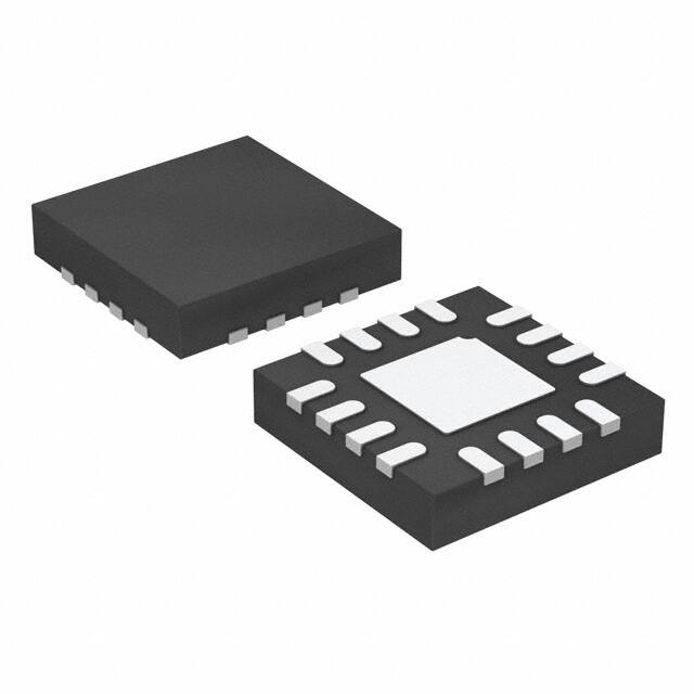
Tiny footprint: 3-mm × 3-mm WQFN
The ADS7947, ADS7948, and ADS7949 support a
wide analog supply range that supports the full-scale
input range up to 5 V. A simple SPI digital interface,
with a digital supply that can operate as low as 1.65
V, allows for easy interfacing to a wide variety of
digital controllers. Automatic power-down can be
enabled when operating at slower speeds to
dramatically reduce power consumption.
Offered in a tiny 3-mm × 3-mm WQFN package, the
ADS7947, ADS7948, and ADS7949 are fully
specified over the extended temperature range of
–40°C to +125°C and are suitable for a wide variety
of data acquisition applications where high
performance, low power, and small size are key.
2 Applications
•
•
•
•
•
Communication systems
Optical networking
Medical instrumentation
Battery-powered equipment
Data acquisition systems
Device Information(1)
PART NUMBER
ADS794x
PACKAGE
BODY SIZE (NOM)
WQFN (16)
3.00 mm × 3.00 mm
(1) For all available packages, see the orderable addendum at
the end of the data sheet.
ADS794x Block Diagram
CH SEL
AVDD
REF
DVDD
AIN0P
AIN0N
MUX
ADC
AIN1P
AIN1N
CS
SCLK
SDO
PDEN
GND
REFGND
1
An IMPORTANT NOTICE at the end of this data sheet addresses availability, warranty, changes, use in safety-critical applications,
intellectual property matters and other important disclaimers. PRODUCTION DATA.
�ADS7947, ADS7948, ADS7949
SLAS708A – SEPTEMBER 2010 – REVISED SEPTEMBER 2019
www.ti.com
Table of Contents
1
2
3
4
5
6
7
Features ..................................................................
Applications ...........................................................
Description .............................................................
Revision History.....................................................
Device Comparison Table.....................................
Pin Configuration and Functions .........................
Specifications.........................................................
1
1
1
2
4
4
5
7.1 Absolute Maximum Ratings ...................................... 5
7.2 ESD Ratings.............................................................. 5
7.3 Recommended Operating Conditions: ADS794x (12-,
10-, 8-Bit) ................................................................... 5
7.4 Thermal Information .................................................. 6
7.5 Electrical Characteristics: ADS7947 (12-Bit) ............ 6
7.6 Electrical Characteristics: ADS7948 (10-Bit) ............ 8
7.7 Electrical Characteristics: ADS7949 (8-Bit) ............ 10
7.8 Timing Requirements .............................................. 11
7.9 Switching Characteristics ........................................ 12
7.10 Typical Characteristics: ADS7947, ADS7948,
ADS7949.................................................................. 13
7.11 Typical Characteristics: ADS7947 (12-Bit)............ 14
8
8.1
8.2
8.3
8.4
8.5
9
Overview .................................................................
Functional Block Diagram .......................................
Feature Description.................................................
Device Functional Modes........................................
Programming...........................................................
20
20
20
25
26
Application and Implementation ........................ 28
9.1 Application Information............................................ 28
10 Power Supply Recommendations ..................... 30
11 Layout................................................................... 31
11.1 Layout Guidelines ................................................. 31
11.2 Layout Example .................................................... 32
12 Device and Documentation Support ................. 33
12.1
12.2
12.3
12.4
12.5
12.6
Related Links ........................................................
Receiving Notification of Documentation Updates
Community Resources..........................................
Trademarks ...........................................................
Electrostatic Discharge Caution ............................
Glossary ................................................................
33
33
33
33
33
33
13 Mechanical, Packaging, and Orderable
Information ........................................................... 33
Detailed Description ............................................ 20
4 Revision History
NOTE: Page numbers for previous revisions may differ from page numbers in the current version.
Changes from Original (September 2010) to Revision A
Page
•
Added Device Information table, ESD Ratings table, Recommended Operating Conditions table, Switching
Characteristics table, Functional Block Diagram section, Feature Description section, Device Functional Modes
section, Programming section, Application and Implementation section, Power Supply Recommendations section,
Layout section, Device and Documentation Support section, and Mechanical, Packaging, and Orderable Information
section ................................................................................................................................................................................... 1
•
Changed document title.......................................................................................................................................................... 1
•
Changed QFN to WQFN throughout document ..................................................................................................................... 1
•
Added High resolution, high throughput: Features bullet ....................................................................................................... 1
•
Changed temperature range Features bullet from Fully Specified from to Extended temperature range ............................. 1
•
Changed Description section for clarity and changed ADC with an inherent sample-and-hold (S/H) input stage to ADC.... 1
•
Changed page 1 figure and added title .................................................................................................................................. 1
•
Changed title of Family and Ordering Information to Device Comparison Table................................................................... 4
•
Changed thermal symbols for RθJA, RθJC(top), RθJB, and RθJC(bot) ............................................................................................. 6
•
Deleted Full-scale input span, Absolute input range, External Reference, AVDD, and DVDD parameters and
Temperature Range section from Electrical Characteristics: ADS7947 (12-Bit) table ........................................................... 6
•
Deleted Full-scale input span, Absolute input range, External Reference, AVDD, and DVDD parameters and
Temperature Range section from Electrical Characteristics: ADS7948 (10-Bit) table .......................................................... 8
•
Deleted Full-scale input span, Absolute input range, External Reference, AVDD, and DVDD parameters and
Temperature Range section from Electrical Characteristics: ADS7949 (8-Bit) table .......................................................... 10
•
Changed Timing Requirements table: added section titles, moved switching parameters into Switching
Characteristics table ............................................................................................................................................................ 11
•
Changed symbol for Pulse duration, SCLK low parameter from tW1 to tWL .......................................................................... 11
•
Added symbol to SCLK frequency parameter ...................................................................................................................... 11
•
Changed title of PCB Layout/Schematic Guidelines to Layout and changed format of section........................................... 31
2
Submit Documentation Feedback
Copyright © 2010–2019, Texas Instruments Incorporated
Product Folder Links: ADS7947 ADS7948 ADS7949
�ADS7947, ADS7948, ADS7949
www.ti.com
SLAS708A – SEPTEMBER 2010 – REVISED SEPTEMBER 2019
Revision History (continued)
•
Changed Recommended ADC Schematic figure ................................................................................................................. 31
Copyright © 2010–2019, Texas Instruments Incorporated
Product Folder Links: ADS7947 ADS7948 ADS7949
Submit Documentation Feedback
3
�ADS7947, ADS7948, ADS7949
SLAS708A – SEPTEMBER 2010 – REVISED SEPTEMBER 2019
www.ti.com
5 Device Comparison Table
PRODUCT
RESOLUTION (Bits)
INPUT
SAMPLE RATE (MSPS)
ADS7947
12
Unipolar, pseudo-differential
2
ADS7948
10
Unipolar, pseudo-differential
2
ADS7949
8
Unipolar, pseudo-differential
2
6 Pin Configuration and Functions
DVDD
SDO
SCLK
CS
16
15
14
13
RTE Package
16-Pin WQFN
Top View
REF
3
10
NC
REFGND
4
9
NC
8
CH SEL
AIN1P
11
7
2
AIN1N
AVDD
6
PDEN
AIN0N
12
5
1
AIN0P
GND
Pin Functions
PIN NO.
4
PIN NAME
FUNCTION
DESCRIPTION
1
GND
Analog/digital
2
AVDD
Analog
ADC power supply.
3
REF
Analog
ADC positive reference input; decouple this pin with REFGND.
4
REFGND
Analog
Reference return; short to analog ground plane.
5
AIN0P
Analog input
Positive analog input, channel 0.
6
AIN0N
Analog input
Negative analog input, channel 0. The allowable signal swing on this pin is ±0.2V; this pin
can be grounded.
7
AIN1N
Analog input
Negative analog input, channel 1. The allowable signal swing on this pin is ±0.2V; this pin
can be grounded.
8
AIN1P
Analog input
Positive analog input, channel 1.
9
NC
—
Not connected internally, TI recommends externally shorting this pin to GND.
10
NC
—
Not connected internally, TI recommends externally shorting this pin to GND.
Power supply ground; all analog and digital signals are referred with respect to this pin.
11
CH SEL
Digital input
This pin selects the analog input channel.
Low = channel 0, high = channel 1.
TI recommends changing the channel within a window of one clock; from half a clock after
the CS falling edge. This change ensures the settling on the multiplexer output before the
sample start.
12
PDEN
Digital input
This pin enables a power-down feature if this pin is high at the CS rising edge.
13
CS
Digital input
Chip-select signal; active low.
14
SCLK
Digital input
Serial SPI clock.
15
SDO
Digital output
Serial data out.
16
DVDD
Digital
Submit Documentation Feedback
Digital I/O supply.
Copyright © 2010–2019, Texas Instruments Incorporated
Product Folder Links: ADS7947 ADS7948 ADS7949
�ADS7947, ADS7948, ADS7949
www.ti.com
SLAS708A – SEPTEMBER 2010 – REVISED SEPTEMBER 2019
7 Specifications
7.1 Absolute Maximum Ratings
over operating free-air temperature range (unless otherwise noted) (1)
MIN
MAX
UNIT
AINxP to GND or AINxN to GND
–0.3 AVDD + 0.3
V
AVDD to GND or DVDD to GND
–0.3
7
V
Digital input voltage to GND
–0.3 DVDD + 0.3
V
Digital output to GND
–0.3 DVDD + 0.3
V
Operating
–40
125
°C
Storage, Tstg
–65
150
°C
Temperature
(1)
Stresses beyond those listed under Absolute Maximum Ratings may cause permanent damage to the device. These are stress ratings
only, which do not imply functional operation of the device at these or any other conditions beyond those indicated under Recommended
Operating Conditions. Exposure to absolute-maximum-rated conditions for extended periods may affect device reliability.
7.2 ESD Ratings
VALUE
V(ESD)
(1)
(2)
Electrostatic discharge
Human-body model (HBM), per ANSI/ESDA/JEDEC JS-001 (1)
±2000
Charged-device model (CDM), per JEDEC specification JESD22C101 (2)
±500
UNIT
V
JEDEC document JEP155 states that 500-V HBM allows safe manufacturing with a standard ESD control process.
JEDEC document JEP157 states that 250-V CDM allows safe manufacturing with a standard ESD control process.
7.3 Recommended Operating Conditions: ADS794x (12-, 10-, 8-Bit)
over operating free-air temperature range (unless otherwise noted)
PARAMETER
MIN
NOM
MAX
UNIT
POWER SUPPLY
AVDD
Analog supply voltage
2.7
3.3
5.5
V
DVDD
Digital supply voltage
1.65
3.3
AVDD
V
AVDD
V
0
VREF
V
AIN0P, AIN1P
–0.2
AVDD +
0.2
V
AIN0N, AIN1M
–0.2
0.2
–40
125
REFERENCE INPUT
VREF
External reference input
2.5
ANALOG INPUTS
FSR
VIN
Full-scale input span (1)
AINxP – AINxN
Absolute input range
TEMPERATURE RANGE
Temperature range for specified performance
(1)
°C
Ideal input span; does not include gain or offset error.
Copyright © 2010–2019, Texas Instruments Incorporated
Product Folder Links: ADS7947 ADS7948 ADS7949
Submit Documentation Feedback
5
�ADS7947, ADS7948, ADS7949
SLAS708A – SEPTEMBER 2010 – REVISED SEPTEMBER 2019
www.ti.com
7.4 Thermal Information
ADS794x
THERMAL METRIC (1)
RTE (WQFN)
UNIT
16 PINS
RθJA
Junction-to-ambient thermal resistance
54.3
°C/W
RθJC(top)
Junction-to-case (top) thermal resistance
53.7
°C/W
RθJB
Junction-to-board thermal resistance
19.2
°C/W
ψJT
Junction-to-top characterization parameter
0.3
°C/W
ψJB
Junction-to-board characterization parameter
14.5
°C/W
RθJC(bot)
Junction-to-case (bottom) thermal resistance
5.2
°C/W
(1)
For more information about traditional and new thermal metrics, see the Semiconductor and IC Package Thermal Metrics application
report.
7.5 Electrical Characteristics: ADS7947 (12-Bit)
minimum and maximum values at AVDD = 2.7 V to 5.5 V, DVDD = 1.65 V to AVDD, TA = –40°C to +125°C, and
fSAMPLE = 2 MSPS (unless otherwise noted); typical values at AVDD = 3 V, DVDD = 1.8 V, TA = +25°C, and fSAMPLE = 2 MSPS
PARAMETER
TEST CONDITIONS
MIN
TYP
MAX
UNIT
ANALOG INPUT
Input capacitance (1)
Input leakage current
At +125°C
32
pF
1.5
nA
12
Bits
SYSTEM PERFORMANCE
Resolution
No missing codes
12
Integral linearity
–1
±0.3
1
LSB (2)
Bits
Differential linearity
–1
±0.3
1
LSB
Offset error (3)
–1
±0.3
1
LSB
Gain error
–1
±0.3
Transition noise
Power-supply rejection
1
LSB
25
µVRMS
60
dB
SAMPLING DYNAMICS
Conversion time
13.5
Acquisition time
80
Maximum sample rate (throughput rate)
SCLK
ns
34-MHz SCLK with a 16-clock frame
34-MHz SCLK and CS low for 13.5 clocks
Aperture delay
2
MSPS
2.1
MSPS
5
ns
Aperture jitter
10
ps
Step response
80
ns
Overvoltage recovery
80
ns
–85
dB
73
dB
dB
DYNAMIC CHARACTERISTICS
Total harmonic distortion (THD) (4)
100kHz
Signal-to-noise ratio (SNR)
100 kHz
Signal-to-noise and distortion ratio (SINAD)
100 kHz
72.75
Spurious-free dynamic range (SFDR)
100 kHz
86
dB
Full-power bandwidth
At –3 dB
15
MHz
72
DIGITAL INPUT/OUTPUT
Logic family
(1)
(2)
(3)
(4)
6
CMOS
See Figure 40 for sampling circuit details.
LSB means least significant bit.
Measured relative to an ideal full-scale input.
Calculated on the first nine harmonics of the input frequency.
Submit Documentation Feedback
Copyright © 2010–2019, Texas Instruments Incorporated
Product Folder Links: ADS7947 ADS7948 ADS7949
�ADS7947, ADS7948, ADS7949
www.ti.com
SLAS708A – SEPTEMBER 2010 – REVISED SEPTEMBER 2019
Electrical Characteristics: ADS7947 (12-Bit) (continued)
minimum and maximum values at AVDD = 2.7 V to 5.5 V, DVDD = 1.65 V to AVDD, TA = –40°C to +125°C, and
fSAMPLE = 2 MSPS (unless otherwise noted); typical values at AVDD = 3 V, DVDD = 1.8 V, TA = +25°C, and fSAMPLE = 2 MSPS
PARAMETER
TEST CONDITIONS
VIH
Logic level
Input leakage current
MIN
TYP
MAX
0.7DVDD
UNIT
V
VIL
0.3DVDD
VOH
ISOURCE = 200 µA
DVDD – 0.2
VOL
ISINK = 200 µA
IIH, IIL
0 < VIN < DVDD
±20
AVDD = 3.3 V, fSAMPLE = 2 MSPS
2.5
V
V
0.4
V
nA
POWER-SUPPLY REQUIREMENTS
IDYNAMIC
AVDD supply current
ISTATIC
DVDD supply current (5)
Power-down state
AVDD supply current
AVDD = 5 V, fSAMPLE = 2 MSPS
AVDD = 3.3 V, SCLK off
1.8
AVDD = 5 V, SCLK off
1.9
DVDD = 3.3 V, SCLK = 34 MHz,
SDO load 20 pF
500
mA
3.5
mA
mA
2.5
mA
µA
IPD-DYNAMIC
SCLK = 34 MHz
550
µA
IPD-STATIC
SCLK off
2.5
µA
1
µs
Power-up time
(5)
3
DVDD consumes only dynamic current. IDVDD = CLOAD × DVDD × number of 0→1 transitions in SDO × fSAMPLE. This current is loaddependent and there is no DVDD current when the output is not toggling.
Copyright © 2010–2019, Texas Instruments Incorporated
Product Folder Links: ADS7947 ADS7948 ADS7949
Submit Documentation Feedback
7
�ADS7947, ADS7948, ADS7949
SLAS708A – SEPTEMBER 2010 – REVISED SEPTEMBER 2019
www.ti.com
7.6 Electrical Characteristics: ADS7948 (10-Bit)
minimum and maximum values at AVDD = 2.7 V to 5.5 V, DVDD = 1.65 V to AVDD, TA = –40°C to +125°C, and
fSAMPLE = 2 MSPS (unless otherwise noted); typical values at AVDD = 3 V, DVDD = 1.8 V, TA = +25°C, and fSAMPLE = 2 MSPS
PARAMETER
TEST CONDITIONS
MIN
TYP
MAX
UNIT
ANALOG INPUT
Input capacitance (1)
Input leakage current
At +125°C
32
pF
1.5
nA
10
Bits
SYSTEM PERFORMANCE
Resolution
No missing codes
10
Bits
Integral linearity
–0.5
±0.15
0.5
LSB (2)
Differential linearity
–0.5
±0.15
0.5
LSB
–0.5
±0.15
0.5
LSB
–0.5
±0.15
0.5
LSB
25
µVRMS
Offset error
(3)
Gain error
Transition noise
Power-supply rejection
60
dB
SAMPLING DYNAMICS
Conversion time
10.5
Acquisition time
80
Maximum sample rate (throughput rate)
SCLK
ns
34-MHz SCLK in 16-clock frame
34-MHz SCLK and CS low for 10.5 clocks
Aperture delay
2
MSPS
2.57
MSPS
5
ns
Aperture jitter
10
ps
Step response
80
ns
Overvoltage recovery
80
ns
–80
dB
DYNAMIC CHARACTERISTICS
Total harmonic distortion (THD) (4)
100kHz
Signal-to-noise ratio (SNR)
100 kHz
Signal-to-noise and distortion ratio (SINAD)
100 kHz
61
Spurious-free dynamic range (SFDR)
100 kHz
81
dB
Full-power bandwidth
At –3 dB
15
MHz
61
dB
dB
DIGITAL INPUT/OUTPUT
Logic family
CMOS
VIH
Logic level
Input leakage current
(1)
(2)
(3)
(4)
8
0.7DVDD
V
VIL
0.3DVDD
VOH
ISOURCE = 200 µA
VOL
ISINK = 200 µA
IIH, IIL
0 < VIN < DVDD
DVDD – 0.2
V
V
0.4
V
±20
nA
See Figure 40 for sampling circuit details.
LSB means least significant bit.
Measured relative to an ideal full-scale input.
Calculated on the first nine harmonics of the input frequency.
Submit Documentation Feedback
Copyright © 2010–2019, Texas Instruments Incorporated
Product Folder Links: ADS7947 ADS7948 ADS7949
�ADS7947, ADS7948, ADS7949
www.ti.com
SLAS708A – SEPTEMBER 2010 – REVISED SEPTEMBER 2019
Electrical Characteristics: ADS7948 (10-Bit) (continued)
minimum and maximum values at AVDD = 2.7 V to 5.5 V, DVDD = 1.65 V to AVDD, TA = –40°C to +125°C, and
fSAMPLE = 2 MSPS (unless otherwise noted); typical values at AVDD = 3 V, DVDD = 1.8 V, TA = +25°C, and fSAMPLE = 2 MSPS
PARAMETER
TEST CONDITIONS
MIN
TYP
MAX
UNIT
POWER-SUPPLY REQUIREMENTS
IDYNAMIC
AVDD supply current
ISTATIC
DVDD supply current
Power-down state
AVDD supply current
(5)
AVDD = 3.3 V, fSAMPLE = 2 MSPS
AVDD = 5 V, fSAMPLE = 2 MSPS
AVDD = 3.3 V, SCLK off
3
mA
3.5
1.8
AVDD = 5 V, SCLK off
1.9
DVDD = 3.3 V, SCLK = 34 MHz,
SDO load 20 pF
500
mA
mA
2.5
mA
µA
IPD-DYNAMIC
SCLK = 34 MHz
550
µA
IPD-STATIC
SCLK off
2.5
µA
1
µs
Power-up time
(5)
2.5
DVDD consumes only dynamic current. IDVDD = CLOAD × DVDD × number of 0→1 transitions in SDO × fSAMPLE. This current is loaddependent and there is no DVDD current when the output is not toggling.
Copyright © 2010–2019, Texas Instruments Incorporated
Product Folder Links: ADS7947 ADS7948 ADS7949
Submit Documentation Feedback
9
�ADS7947, ADS7948, ADS7949
SLAS708A – SEPTEMBER 2010 – REVISED SEPTEMBER 2019
www.ti.com
7.7 Electrical Characteristics: ADS7949 (8-Bit)
minimum and maximum values at AVDD = 2.7 V to 5.5 V, DVDD = 1.65 V to AVDD, TA = –40°C to +125°C, and
fSAMPLE = 2 MSPS (unless otherwise noted); typical values at AVDD = 3 V, DVDD = 1.8 V, TA = +25°C, and fSAMPLE = 2 MSPS
PARAMETER
TEST CONDITIONS
MIN
TYP
MAX
UNIT
ANALOG INPUT
Input capacitance (1)
Input leakage current
At +125°C
32
pF
1.5
nA
8
Bits
SYSTEM PERFORMANCE
Resolution
No missing codes
8
Bits
Integral linearity
–0.3
±0.06
0.3
LSB (2)
Differential linearity
–0.3
±0.06
0.3
LSB
–0.3
±0.06
0.3
LSB
–0.3
±0.06
0.3
LSB
25
µVRMS
Offset error
(3)
Gain error
Transition noise
Power-supply rejection
60
dB
SAMPLING DYNAMICS
Conversion time
8.5
Acquisition time
80
Maximum sample rate (throughput rate)
SCLK
ns
34-MHz SCLK in 16-clock frame
2
MSPS
34-MHz SCLK and CS low for 8.5 clocks
3
MSPS
5
ns
Aperture delay
Aperture jitter
10
ps
Step response
80
ns
Overvoltage recovery
80
ns
–80
dB
DYNAMIC CHARACTERISTICS
Total harmonic distortion (THD) (4)
100 kHz
Signal-to-noise ratio (SNR)
100 kHz
Signal-to-noise and distortion ratio (SINAD)
100 kHz
49
Spurious-free dynamic range (SFDR)
100 kHz
81
dB
Full-power bandwidth
At –3 dB
15
MHz
49
dB
dB
DIGITAL INPUT/OUTPUT
Logic family
CMOS
VIH
Logic level
Input leakage current
(1)
(2)
(3)
(4)
10
0.7DVDD
V
VIL
0.3DVDD
VOH
ISOURCE = 200 µA
VOL
ISINK = 200 µA
IIH, IIL
0 0.2 V so that the REF50xx functions
properly.
Figure 42. Typical Reference Driving Circuit
22
Submit Documentation Feedback
Copyright © 2010–2019, Texas Instruments Incorporated
Product Folder Links: ADS7947 ADS7948 ADS7949
�ADS7947, ADS7948, ADS7949
www.ti.com
SLAS708A – SEPTEMBER 2010 – REVISED SEPTEMBER 2019
Feature Description (continued)
8.3.3 Clock
The ADS794x use SCLK for conversions (typically 34 MHz). A lower frequency SCLK can be used for
applications requiring sample rates less than 2 MSPS. However, using a 34-MHz SCLK and slowing down the
device speed by choosing a lower frequency for CS is better, which allows more acquisition time. This
configuration relaxes constraints on the output impedance of the driving circuit. See the Application Information
section for a calculation of the driving circuit output impedance.
8.3.4 ADC Transfer Function
The ADS7947 (12 bit), ADS7948 (10 bit), and ADS7949 (8 bit) devices are unipolar, pseudo-differential input
devices. The ADC output is in straight binary format. Figure 43 shows ideal characteristics for this family of
devices. Here, FSR is the full-scale range for the ADC input (AINxP – AINxN) and is equal to the reference input
voltage to the ADC (VREF). 1 LSB is equal to (VREF / 2N) where N is the resolution of the ADC (for example, N =
12 for the ADS7947).
ADC Code
111¼111
100¼000
000¼001
1LSB
FSR/2
FSR - 1LSB
Analog Input
Figure 43. ADS7947, ADS7948, and ADS7949 Transfer Characteristics
8.3.5 Power-Down
The ADS7947, ADS7948, and ADS7949 family of devices offers an easy-to-use power-down feature available
through a dedicated PDEN pin (pin 12). A high level on PDEN at the CS rising edge enables the power-down
mode for that particular cycle. Figure 44 to Figure 46 illustrate device operation with power-down in both 32-clock
and 16-clock mode.
Many applications must slow device operation. For speeds below approximately 500 kSPS, the 32-clock mode
can be used with power-down. This capability results in considerable power savings.
As illustrated in Figure 44, PDEN is held at a logic '1' level. The device observes the PDEN status only at the CS
rising edge; however, for continuous low-speed operation, continuously hold PDEN = 1. The devices detect
power-down mode on the CS rising edge with PDEN = 1.
Copyright © 2010–2019, Texas Instruments Incorporated
Product Folder Links: ADS7947 ADS7948 ADS7949
Submit Documentation Feedback
23
�ADS7947, ADS7948, ADS7949
SLAS708A – SEPTEMBER 2010 – REVISED SEPTEMBER 2019
www.ti.com
Feature Description (continued)
tACQ
tCONV
11th and 9th SCLK rising edge for 10- and 8-bit devices, respectively.
CS
SCLK
tACQ (min)+ 1ms
1
2
14
15
16
D11
SDO
18
27
28
29
D10
D2
D1
D0
17
30
31
32
Data from Sample N
Power-Down
State
(Internal)
Active
Power-Down
Active
IDYNAMIC
ISTATIC
IAVDD
Profile
IPD-STATIC if
SCLK is off;
otherwise,
IPD-DYNAMIC.
IPD-DYNAMIC
Figure 44. Operation With a 32-Clock Frame in Power-Down Mode (PDEN = 1)
On the CS falling edge, the devices start normal operation as previously described. The devices complete
conversions on the 14th SCLK rising edge. (Conversions complete on the 11th and ninth SCLK rising edge for
10-bit and 8-bit devices, respectively.) The devices enter the power-down state immediately after conversions
complete. However, the devices can still output data as per the timings described previously. The devices
consume dynamic power-down current (IPD-DYNAMIC) during data out operations. TI recommends stopping the
clock after the 32nd SCLK falling edge to further save power down to the static power-down current level (IPDSTATIC). The devices power up again on the SCLK rising edge. However, they require an extra 1µs to power up
completely. CS must be high for the 1µs + tACQ (min) period.
In some applications, data collection is accomplished in burst mode. The system powers down after data
collection. 16-clock mode is convenient for these applications. Figure 45 and Figure 46 detail power saving in 16clock burst mode.
As illustrated in Figure 45, the two frames capturing the N–1 and Nth samples are normal 16-clock frames.
Keeping PDEN = 1 prior to the CS rising edge in the next frame ensures that the devices detect the power-down
mode. Data from the Nth sample are read during this frame. The Nth sample represents the last data of interest
in the burst of conversions. The devices enter power-down state after the end of conversions. This state is the
14th, 11th, or ninth SCLK rising edge for the 12-, 10-, and 8-bit devices, respectively. The clock can be stopped
after the 14th SCLK falling edge; however, TI still recommends stopping the clock after the 16th SCLK falling
edge. There must be no more than 29 SCLK falling edges during the CS low period. This limitation ensures that
the devices remain in 16-clock mode.
The devices remain in a power-down state as long as CS is low. A CS rising edge with PDEN = 0 brings the
devices out of the power-down state. Ensure that the CS high time for the first sample after power up is more
than 1 µs + tACQ (min).
24
Submit Documentation Feedback
Copyright © 2010–2019, Texas Instruments Incorporated
Product Folder Links: ADS7947 ADS7948 ADS7949
�ADS7947, ADS7948, ADS7949
www.ti.com
SLAS708A – SEPTEMBER 2010 – REVISED SEPTEMBER 2019
Feature Description (continued)
tPDSU
tPDH
PDEN
Sample
N-1
Dummy
Sample
Sample
N
CS
SCLK
1
15
2
16
1
2
15
16
1
11
2
12
13
14
15
16
SDO
Data from Sample
N-2
Data from Sample
N-1
Data from Sample
N
Power-Down
State
(Internal)
Active
Power-Down
Figure 45. Entry Into Power-Down With 16-Clock Burst Mode
tPDSU
PDEN
Sample
N+1
CS
Sample
N+3
Sample
N+2
tACQ (min) + 1ms
1
SCLK
2
15
16
1
2
15
16
1
2
SDO
Invalid Data
Power-Down
State
(Internal)
Power-Down
Data from Sample
N+1
Data from Sample
N+2
Active
Figure 46. Exit From Power-Down With 16-Clock Burst Mode
8.4 Device Functional Modes
8.4.1 Device Operation
The ADS7947, ADS7948, and ADS7949 are typically operated with either a 16-clock frame or 32-clock frame for
ease of interfacing with the host processor.
Copyright © 2010–2019, Texas Instruments Incorporated
Product Folder Links: ADS7947 ADS7948 ADS7949
Submit Documentation Feedback
25
�ADS7947, ADS7948, ADS7949
SLAS708A – SEPTEMBER 2010 – REVISED SEPTEMBER 2019
www.ti.com
8.5 Programming
8.5.1 16-Clock Frame
Figure 47 through Figure 49 illustrate the devices operating in 16-clock mode. This mode is the fastest mode for
device operation. In this mode, the devices output data from previous conversions while converting the recently
sampled signal.
As shown in Figure 47, the ADS7947 starts acquisition of the analog input from the 14th rising edge of SCLK.
The device samples the input signal on the CS falling edge. SDO comes out of 3-state and the device outputs
the MSB on the CS falling edge. The device outputs the next lower SDO bits on every SCLK falling edge after
the SCLK rising edge. The data correspond to the sample and conversion completed in the previous frame.
During a CS low period, the device converts the recently sampled signal and uses SCLK for conversions. The
number of clocks needed for a conversion for 12-bit and 8-bit devices are different. For the ADS7947, conversion
is complete on the 14th SCLK rising edge. CS can be high at any time after the 14th SCLK rising edge. The CS
rising edge after the 14th SCLK rising edge and before the 29th SCLK falling edge keeps the device in the 16clock data frame. The device output goes to 3-state with CS high.
Sample
N
Sample
N+1
tACQ
tCONV
CS
1
SCLK
SDO
D11
2
3
4
5
6
7
8
9
10
11
12
D10
D9
D8
D7
D6
D5
D4
D3
D2
D1
D0
13
14
15
16
Data from Sample N-1
Figure 47. ADS7947 Operating in 16-Clock Mode Without Power-Down (PDEN = 0)
SCLK can also be stopped after the 14th SCLK rising edge.
Figure 48 and Figure 49 illustrate the 16-clock mode operation for the ADS7948 and ADS7949, respectively. The
operation for these 10-bit and 8-bit devices is identical to the ADS7947 except that the conversion ends on
different edges of SCLK. For the ADS7948, the conversion ends and acquisition starts on the 11th SCLK rising
edge. For the ADS7949, the device uses the ninth SCLK rising edge for the conversion end and acquisition start.
Similar to the ADS7947, CS can go high and SCLK can be stopped when the device enters acquisition.
Sample
N
Sample
N+1
tACQ
tCONV
CS
SCLK
1
2
3
4
5
6
7
8
9
10
SDO
D9
D8
D7
D6
D5
D4
D3
D2
D1
D0
11
12
13
14
15
16
Data from Sample N-1
Figure 48. ADS7948 Operating in 16-Clock Mode Without Power-Down (PDEN = 0)
26
Submit Documentation Feedback
Copyright © 2010–2019, Texas Instruments Incorporated
Product Folder Links: ADS7947 ADS7948 ADS7949
�ADS7947, ADS7948, ADS7949
www.ti.com
SLAS708A – SEPTEMBER 2010 – REVISED SEPTEMBER 2019
Programming (continued)
Sample
N
Sample
N+1
tACQ
tCONV
CS
SCLK
1
2
3
4
5
6
7
8
SDO
D7
D6
D5
D4
D3
D2
D1
D0
9
10
11
12
13
14
15
16
Data from Sample N-1
Figure 49. ADS7949 Operating in 16-Clock Mode Without Power-Down (PDEN = 0)
8.5.2 32-Clock Frame
Figure 50 through Figure 52 illustrate the devices operating in 32-clock mode. In this mode, the devices convert
and output the data from the most recent sample before taking the next sample.
Sample
N
Sample
N+1
tACQ
tCONV
CS
SCLK
1
2
14
15
16
17
D11
SDO
18
23
24
25
26
27
28
D10
D5
D4
D3
D2
D1
D0
29
30
31
32
Data from Sample N
Figure 50. ADS7947 Operation in 32-Clock Frame Without Power-Down (PDEN = 0)
Sample
N
Sample
N+1
tACQ
tCONV
CS
SCLK
1
2
11
12
16
SDO
17
18
23
24
25
26
D9
D8
D3
D2
D1
D0
27
28
29
30
31
32
Data from Sample N
Figure 51. ADS7948 Operating in 32-Clock Frame Without Power-Down (PDEN = 0)
Copyright © 2010–2019, Texas Instruments Incorporated
Product Folder Links: ADS7947 ADS7948 ADS7949
Submit Documentation Feedback
27
�ADS7947, ADS7948, ADS7949
SLAS708A – SEPTEMBER 2010 – REVISED SEPTEMBER 2019
www.ti.com
Programming (continued)
Sample
N
Sample
N+1
tACQ
tCONV
CS
SCLK
1
2
9
10
16
SDO
17
18
23
24
D7
D6
D1
D0
25
26
27
28
29
30
31
32
Data from Sample N
Figure 52. ADS7949 Operating in 32-Clock Frame Without Power-Down (PDEN = 0)
CS can be held low past the 16th falling edge of SCLK. The device continues to output recently converted data
starting with the 16th SCLK falling edge. If CS is held low until the 30th SCLK falling edge, then the device
detects 32-clock mode. The device data from recent conversions are already out with no latency before the 30th
SCLK falling edge. When 32-clock mode is detected, the device outputs 16 zeros during the next conversion (in
fact, for the first 16 clocks), unlike 16-clock mode where the device outputs the previous conversion result. SCLK
can be stopped after the device has seen the 30th falling edge with CS low.
9 Application and Implementation
NOTE
Information in the following applications sections is not part of the TI component
specification, and TI does not warrant its accuracy or completeness. TI’s customers are
responsible for determining suitability of components for their purposes. Customers should
validate and test their design implementation to confirm system functionality.
9.1 Application Information
The device employs a sample-and-hold stage at the input; see Figure 40 for a typical equivalent circuit of a
sample-and-hold stage. The device connects a 32-pF sampling capacitor during sampling. This configuration
results in a glitch at the input terminals of the device at the start of the sample. The external circuit must be
designed in such a way that the input can settle to the required accuracy during the sampling time chosen.
Figure 53 shows a typical driving circuit for the analog inputs.
0V to VREF
+VA
+
5W
OPA365
AVDD
AINxP
50W
470pF
ADS7947
ADS7948
ADS7949
AINxN
5W
GND
Figure 53. Typical Input Driving Circuit
28
Submit Documentation Feedback
Copyright © 2010–2019, Texas Instruments Incorporated
Product Folder Links: ADS7947 ADS7948 ADS7949
�ADS7947, ADS7948, ADS7949
www.ti.com
SLAS708A – SEPTEMBER 2010 – REVISED SEPTEMBER 2019
Application Information (continued)
The 470-pF capacitor across the AINxP and AINxN terminals decouples the driving op amp from the sampling
glitch. Splitting the series resistance of the input filter in two equal values is recommended, as shown in
Figure 53. Both input terminals are recommended to have the same impedance from the external circuit. The
low-pass filter at the input limits noise bandwidth of the driving op amp. Select the filter bandwidth so that the fullscale step at the input can settle to the required accuracy during the sampling time. Equation 1, Equation 2, and
Equation 3 are useful for filter component selection.
Sampling Time
Filter Time Constant (tAU) =
Settling Resolution ´ ln(2)
Where:
Settling resolution is the accuracy in LSB to which the input needs to settle. A typical settling resolution
for the 12-bit device is 13 or 14.
(1)
Filter Time Constant (tAU) = R ´ C
(2)
1
Filter Bandwidth =
2 ´ p ´ tAU
(3)
Also, make sure the driving op amp bandwidth does not limit the signal bandwidth below filter bandwidth. In
many applications, signal bandwidth can be much lower than filter bandwidth. In this case, an additional low-pass
filter can be used at the input of the driving op amp. This signal filter bandwidth can be selected in accordance
with the input signal bandwidth.
9.1.1 Driving an ADC Without a Driving Op Amp
There are some low input signal bandwidth applications, such as battery power monitoring or mains monitoring.
For these applications, an ADC does not have to be operated at high sampling rates and, preferrably, avoid
using a driving op amp from a cost perspective. In this case, the ADC input observes the impedance of the signal
source (such as a battery or mains transformer). This section elaborates the effects of source impedance on
sampling frequency.
Equation 1 can be rewritten as Equation 4:
Sampling Time = Filter Time Constant × Settling Resolution × ln(2)
(4)
As shown in Figure 54, use a bypass capacitor across the positive and negative ADC input terminals.
+VA
RSOURCE
AVDD
AINxP
ADS7947
ADS7948
ADS7949
CBYPASS
AINxN
Signal
Source
R1
5W
GND
Figure 54. Driving an ADC Without a Driving Op Amp
Source impedance (RSOURCE + R1) with (CBYPASS + CSAMPLE) acts as a low-pass filter with Equation 5:
Filter Time Constant = (RSOURCE + R1) × (CBYPASS + CSAMPLE)
Where:
CSAMPLE is the internal sampling capacitance of the ADC (equal to 32 pF).
(5)
Table 1 lists the recommended bypass capacitor values and the filter time constant for different source
resistances. Use a 10-pF bypass capacitor, at minimum.
Copyright © 2010–2019, Texas Instruments Incorporated
Product Folder Links: ADS7947 ADS7948 ADS7949
Submit Documentation Feedback
29
�ADS7947, ADS7948, ADS7949
SLAS708A – SEPTEMBER 2010 – REVISED SEPTEMBER 2019
www.ti.com
Application Information (continued)
Table 1. Filter Time Constant versus Source Resistance
RSOURCE (Ω)
RSOURCE + R1
APPROXIMATE CBYPASS
(pF)
CBYPASS + CSAMPLE (pF)
FILTER TIME
CONSTANT (ns)
15
20
370
400
8
25
30
235
267
8
50
55
115
145
8
100
105
44
76
8
180
185
10
43.2
8
10.7
250
255
10
42
1000
1005
10
42
42.2
5000
5005
10
42
210.2
Typically, settling resolution is selected as (ADC resolution + 2). For the ADS7947 (12-bit) the ideal settling
resolution is 14. Using equations Equation 2 and Equation 3, the sampling time can be easily determined for a
given source impedance. This resolution allows 80 ns of sampling time for a 12-bit ADC with 8 ns of filter time
constant, which matches the ADS7947 specifications. For source impedances above 180 Ω, the filter time
constant continues to increase beyond the 8 ns required for an 80-ns sampling time. This incrementation
increases the minimum permissible sampling time for the 12-bit settling and the device must be operated at a
lower sampling rate.
The device sampling rate can be maximized by using a 34-MHz clock even for lower throughputs. Table 2 shows
typical calculations for the ADS7947(12-bit).
Table 2. Sampling Frequency versus Source Impedance for the ADS7947 (12-Bit)
RSOURCE (Ω)
CBYPASS (pF)
SAMPLING TIME,
tACQ (ns)
CONVERSION TIME, CYCLE TIME, tACQ +
tCONV (ns)
tCONV (ns)
SAMPLING RATE
(MSPS)
180
10
80
397
(with 34MHz clock)
477
2
250
10
107
397
(with 34MHz clock)
504
1.98
1000
10
422
397
(with 34MHz clock)
819
1.2
5000
10
2102
397
(with 34MHz clock)
2499
0.4
An 1000-ns additional sampling time must be allowed over what is shown in Table 2 if PDEN (pin 12) is set high.
10 Power Supply Recommendations
The device has two separate power supplies: AVDD and DVDD. The device operates on AVDD; DVDD is used
for the interface circuits. AVDD and DVDD can be independently set to any value within the permissible ranges.
Decouple the AVDD and DVDD pins individually with 1-µF ceramic decoupling capacitors. The decoupling
capacitors must be placed as close as possible to the device.
30
Submit Documentation Feedback
Copyright © 2010–2019, Texas Instruments Incorporated
Product Folder Links: ADS7947 ADS7948 ADS7949
�ADS7947, ADS7948, ADS7949
www.ti.com
SLAS708A – SEPTEMBER 2010 – REVISED SEPTEMBER 2019
11 Layout
11.1 Layout Guidelines
ADCs are mixed-signal devices. For maximum performance, proper decoupling, grounding, and proper
termination of digital signals is essential. Figure 55 shows the essential components around the ADC. All
capacitors shown are ceramic. These decoupling capacitors must be placed close to the respective signal pins.
There is a 47-Ω source series termination resistor shown on the SDO signal. This resistor must be placed as
close to pin 15 as possible. Series terminations for SCLK and CS must be placed close to the host.
Analog supply
Reference input
1 µF
C4
GND
1
3
4
2
AVDD
Common analog and digital
ground plane
REF
REFGND
1 µF
C3
0.1 µF
C5
Input
signal
DVDD
AIN0P
5
16
5
5
470 pF
C2
1 µF
C6
Digital supply
SDO
AIN0N
15
ADS7947
6
47
R1
ADS7948
AIN1N
SCLK
AIN1P
13
12
CS
PDEN
10
NC
NC
11
8
9
470 pF
C1
Digital signals from host
Input
signal
5
14
ADS7949
7
CH SEL
5
Figure 55. Recommended ADC Schematic
Copyright © 2010–2019, Texas Instruments Incorporated
Product Folder Links: ADS7947 ADS7948 ADS7949
Submit Documentation Feedback
31
�ADS7947, ADS7948, ADS7949
SLAS708A – SEPTEMBER 2010 – REVISED SEPTEMBER 2019
www.ti.com
11.2 Layout Example
A common ground plane for both analog and digital often gives better results. Typically, the second PCB layer is
the ground plane. The ADC ground pins are returned to the ground plane through multiple vias (PTH). Good
practice is to place analog components on one side and digital components on other side of the ADC (or ADCs).
All signals must be routed, assuming there is a split ground plane for analog and digital. Furthermore, splitting
the ground initially during layout is better. Route all analog and digital traces so that the traces see the respective
ground all along the second layer. Then short both grounds to form a common ground plane. Figure 56 shows a
typical layout around the ADC.
Figure 56. Recommended ADC Layout
(Only top layer is shown, second layer is common ground for analog and digital)
32
Submit Documentation Feedback
Copyright © 2010–2019, Texas Instruments Incorporated
Product Folder Links: ADS7947 ADS7948 ADS7949
�ADS7947, ADS7948, ADS7949
www.ti.com
SLAS708A – SEPTEMBER 2010 – REVISED SEPTEMBER 2019
12 Device and Documentation Support
12.1 Related Links
The table below lists quick access links. Categories include technical documents, support and community
resources, tools and software, and quick access to order now.
Table 3. Related Links
PARTS
PRODUCT FOLDER
ORDER NOW
TECHNICAL
DOCUMENTS
TOOLS &
SOFTWARE
SUPPORT &
COMMUNITY
ADS7947
Click here
Click here
Click here
Click here
Click here
ADS7948
Click here
Click here
Click here
Click here
Click here
ADS7949
Click here
Click here
Click here
Click here
Click here
12.2 Receiving Notification of Documentation Updates
To receive notification of documentation updates, navigate to the device product folder on ti.com. In the upper
right corner, click on Alert me to register and receive a weekly digest of any product information that has
changed. For change details, review the revision history included in any revised document.
12.3 Community Resources
TI E2E™ support forums are an engineer's go-to source for fast, verified answers and design help — straight
from the experts. Search existing answers or ask your own question to get the quick design help you need.
Linked content is provided "AS IS" by the respective contributors. They do not constitute TI specifications and do
not necessarily reflect TI's views; see TI's Terms of Use.
12.4 Trademarks
E2E is a trademark of Texas Instruments.
All other trademarks are the property of their respective owners.
12.5 Electrostatic Discharge Caution
This integrated circuit can be damaged by ESD. Texas Instruments recommends that all integrated circuits be handled with
appropriate precautions. Failure to observe proper handling and installation procedures can cause damage.
ESD damage can range from subtle performance degradation to complete device failure. Precision integrated circuits may be more
susceptible to damage because very small parametric changes could cause the device not to meet its published specifications.
12.6 Glossary
SLYZ022 — TI Glossary.
This glossary lists and explains terms, acronyms, and definitions.
13 Mechanical, Packaging, and Orderable Information
The following pages include mechanical, packaging, and orderable information. This information is the most
current data available for the designated devices. This data is subject to change without notice and revision of
this document. For browser-based versions of this data sheet, refer to the left-hand navigation.
Copyright © 2010–2019, Texas Instruments Incorporated
Product Folder Links: ADS7947 ADS7948 ADS7949
Submit Documentation Feedback
33
�PACKAGE OPTION ADDENDUM
www.ti.com
10-Dec-2020
PACKAGING INFORMATION
Orderable Device
Status
(1)
Package Type Package Pins Package
Drawing
Qty
Eco Plan
(2)
Lead finish/
Ball material
MSL Peak Temp
Op Temp (°C)
Device Marking
(3)
(4/5)
(6)
ADS7947SRTER
ACTIVE
WQFN
RTE
16
3000
RoHS & Green
NIPDAU
Level-2-260C-1 YEAR
-40 to 125
7947
ADS7947SRTET
ACTIVE
WQFN
RTE
16
250
RoHS & Green
NIPDAU
Level-2-260C-1 YEAR
-40 to 125
7947
ADS7948SRTER
ACTIVE
WQFN
RTE
16
3000
RoHS & Green
NIPDAU
Level-2-260C-1 YEAR
-40 to 125
7948
ADS7948SRTET
ACTIVE
WQFN
RTE
16
250
RoHS & Green
NIPDAU
Level-2-260C-1 YEAR
-40 to 125
7948
ADS7949SRTER
ACTIVE
WQFN
RTE
16
3000
RoHS & Green
NIPDAU
Level-2-260C-1 YEAR
-40 to 125
7949
ADS7949SRTET
ACTIVE
WQFN
RTE
16
250
RoHS & Green
NIPDAU
Level-2-260C-1 YEAR
-40 to 125
7949
(1)
The marketing status values are defined as follows:
ACTIVE: Product device recommended for new designs.
LIFEBUY: TI has announced that the device will be discontinued, and a lifetime-buy period is in effect.
NRND: Not recommended for new designs. Device is in production to support existing customers, but TI does not recommend using this part in a new design.
PREVIEW: Device has been announced but is not in production. Samples may or may not be available.
OBSOLETE: TI has discontinued the production of the device.
(2)
RoHS: TI defines "RoHS" to mean semiconductor products that are compliant with the current EU RoHS requirements for all 10 RoHS substances, including the requirement that RoHS substance
do not exceed 0.1% by weight in homogeneous materials. Where designed to be soldered at high temperatures, "RoHS" products are suitable for use in specified lead-free processes. TI may
reference these types of products as "Pb-Free".
RoHS Exempt: TI defines "RoHS Exempt" to mean products that contain lead but are compliant with EU RoHS pursuant to a specific EU RoHS exemption.
Green: TI defines "Green" to mean the content of Chlorine (Cl) and Bromine (Br) based flame retardants meet JS709B low halogen requirements of