Order
Now
Product
Folder
Support &
Community
Tools &
Software
Technical
Documents
Reference
Design
AFE031
SBOS531E – AUGUST 2010 – REVISED JUNE 2019
AFE031 Powerline Communications Analog Front-End
1 Features
3 Description
•
The AFE031 is a low-cost, integrated, powerline
communications (PLC) analog front-end (AFE) device
that is capable of capacitive- or transformer-coupled
connections to the powerline while under the control
of a DSP or microcontroller. It is ideal for driving lowimpedance lines that require up to 1.5 A into reactive
loads. The integrated receiver is able to detect
signals down to 20 μVRMS and is capable of a wide
range of gain options to adapt to varying input signal
conditions. This monolithic integrated circuit provides
high
reliability
in
demanding
powerline
communications applications.
1
•
•
•
•
•
•
•
•
•
•
•
•
•
•
•
Integrated powerline driver with thermal and
overcurrent protection
Conforms to EN50065-1
PRIME certified
Large output swing: 12 VPP at 1.5 A
(15-V supply)
Low power consumption:
15 mW (receive mode)
Programmable Tx and Rx filters
Supports EN50065 CENELEC bands A, B, C, D
Supports FSK, S-FSK, and OFDM
Supports PRIME, G3, IEC 61334
Receive sensitivity: 20 μVRMS, typical
Programmable Tx and Rx gain control
Four-wire serial peripheral interface
Two integrated zero crossing detectors
Two-wire transceiver buffer
48-Pin QFN PowerPAD™ package
Extended junction temperature range:
–40°C to +125°C
The AFE031 transmit power amplifier operates from a
single supply in the range of 7 V to 24 V. At
maximum output current, a wide output swing
provides a 12-VPP (IOUT = 1.5 A) capability with a
nominal 15-V supply. The analog and digital signal
processing circuitry operates from a single 3.3-V
power supply.
Device Information(1)
PART NUMBER
AFE031
PACKAGE
VQFN (48)
BODY SIZE (NOM)
7.00 mm × 7.00 mm
(1) For all available packages, see the orderable addendum at
the end of the data sheet.
2 Applications
E_Rx_OUT
E_Rx_IN
PA_OUT
TSENSE
PA_GND
PA_VS
PA_ISET
ZC_IN1
ZC_IN2
ZC_OUT2
ZC_OUT1
eMetering
Lighting
Solar
Pilot wire
REF1
REF2
•
•
•
•
E_Tx_CLK
DVDD
DGND
AGND1
AVDD1
AGND2
AVDD2
E_Tx_IN
E_Tx_OUT
ZC1
Bias
ZC2
Two-Wire Rx/Tx
RxPGA_1
SCLK
DI
DO
CS
Digital Interface
(SPI)
Power
Amplifier
Rx_PGA1_IN
Rx_PGA1_OUT
Rx_F_IN
DAC
SD
Tx_Flag
Rx_Flag
Rx_C1
Control Register
Rx_C2
Rx Filter
INT
Rx_F_OUT
RxPGA_2
Digital-to-Analog
Converter
TxPGA
Tx Filter
Rx_PGA2_IN
Rx_PGA2_OUT
PA_IN
Tx_F_OUT
Tx_F_IN2
Tx_PGA_OUT
Tx_F_IN1
Tx_PGA_IN
AFE031
1
An IMPORTANT NOTICE at the end of this data sheet addresses availability, warranty, changes, use in safety-critical applications,
intellectual property matters and other important disclaimers. PRODUCTION DATA.
�AFE031
SBOS531E – AUGUST 2010 – REVISED JUNE 2019
www.ti.com
Table of Contents
1
2
3
4
5
6
7
8
Features ..................................................................
Applications ...........................................................
Description .............................................................
Revision History.....................................................
Description, continued ..........................................
Device Comparison Table.....................................
Pin Configuration and Functions .........................
Specifications.........................................................
8.1
8.2
8.3
8.4
8.5
8.6
8.7
8.8
8.9
8.10
8.11
8.12
1
1
1
2
4
5
5
7
Absolute Maximum Ratings ...................................... 7
ESD Ratings.............................................................. 7
Thermal Information .................................................. 8
Electrical Characteristics: Transmitter (Tx) .............. 8
Electrical Characteristics: Power Amplifier (PA) .... 10
Electrical Characteristics: Receiver (Rx)................ 11
Electrical Characteristics: Digital............................ 13
Electrical Characteristics: Two-Wire Interface ....... 14
Electrical Characteristics: Internal Bias Generator 14
Electrical Characteristics: Power Supply ............. 15
Timing Requirements ............................................ 15
Timing Diagrams ................................................... 16
8.13 Typical Characteristics .......................................... 18
9
Detailed Description ............................................ 22
9.1
9.2
9.3
9.4
9.5
9.6
Functional Block Diagram .......................................
Feature Description.................................................
Power Supplies .......................................................
Pin Descriptions ......................................................
Calibration Modes ...................................................
Serial Interface ........................................................
22
23
37
38
40
41
10 Application and Implementation........................ 45
10.1 Application Information.......................................... 45
10.2 Typical Application ................................................ 46
11 Device and Documentation Support ................. 52
11.1
11.2
11.3
11.4
11.5
11.6
11.7
Device Support......................................................
Documentation Support ........................................
Receiving Notification of Documentation Updates
Community Resources..........................................
Trademarks ...........................................................
Electrostatic Discharge Caution ............................
Glossary ................................................................
52
53
53
53
53
53
53
12 Mechanical, Packaging, and Orderable
Information ........................................................... 53
4 Revision History
NOTE: Page numbers for previous revisions may differ from page numbers in the current version.
Changes from Revision D (May 2012) to Revision E
Page
•
Deleted Package/Ordering Information table; see Package Option Addendum at the end of the data sheet ....................... 1
•
Deleted ESD specifications from Absolute Maximum Ratings table. Moved to separate ESD Ratings table. ...................... 7
•
Deleted references to Tx PGA calibration in Calibration Modes .......................................................................................... 40
•
Deleted reference to TX_PGA_CAL in Table 14 ................................................................................................................. 43
Changes from Revision C (March 2012) to Revision D
Page
•
Updated Figure 31................................................................................................................................................................ 28
•
Updated Figure 33................................................................................................................................................................ 30
Changes from Revision B (September 2011) to Revision C
Page
•
Changed transmit power amplifier operating range description in Description section.......................................................... 1
•
Added cross-reference to footnote 2 to Output short-circuit (PA) parameter in Absolute Maximum Ratings table ............... 7
•
Changed Frequency Response, Passband frequency (B/C/D Modes) parameter minimum and typical specifications
in Electrical Characteristics: Receiver (Rx) .......................................................................................................................... 11
•
Deleted Digital Outputs (INT, Tx_Flag, Rx_Flag), INT pin high, INT pin low, Tx_Flag high, Tx_Flag low, Rx_Flag
high, and Rx_Flag low parameter units from Electrical Characteristics: Digital ................................................................... 13
•
Changed Digital Outputs (INT, Tx_Flag, Rx_Flag), Tx_Flag high, Tx_Flag low, Rx_Flag high, and Rx_Flag low
parameter specification descriptions in Electrical Characteristics: Digital............................................................................ 13
•
Changed Operating Supply Range, Power amplifier supply voltage parameter maximum specification in Electrical
Characteristics: Power Supply.............................................................................................................................................. 15
•
Changed title of Figure 20 .................................................................................................................................................... 20
•
Changed description of PA operating range in PA Block section ........................................................................................ 23
2
Submit Documentation Feedback
Copyright © 2010–2019, Texas Instruments Incorporated
Product Folder Links: AFE031
�AFE031
www.ti.com
SBOS531E – AUGUST 2010 – REVISED JUNE 2019
•
Updated Equation 2.............................................................................................................................................................. 24
•
Changed proper design margin note in PA Block section.................................................................................................... 24
•
Updated Figure 34................................................................................................................................................................ 31
•
Changed description of REF1 and REF2 Blocks section ..................................................................................................... 32
•
Changed second paragraph of Power Supplies section ...................................................................................................... 37
•
Changed title of Table 11 ..................................................................................................................................................... 41
Submit Documentation Feedback
Copyright © 2010–2019, Texas Instruments Incorporated
Product Folder Links: AFE031
3
�AFE031
SBOS531E – AUGUST 2010 – REVISED JUNE 2019
www.ti.com
5 Description, continued
The AFE031 is internally protected against overtemperature and short-circuit conditions. It also provides an
adjustable current limit. An interrupt output is provided that indicates both current limit and thermal limit. There is
also a shutdown pin that can be used to quickly put the device into its lowest power state. Through the four-wire
serial peripheral interface, or SPI™, each functional block can be enabled or disabled to optimize power
dissipation.
The AFE031 is housed in a thermally-enhanced, surface-mount PowerPAD package (QFN-48). Operation is
specified over the extended industrial junction temperature range of –40°C to +125°C.
4
Submit Documentation Feedback
Copyright © 2010–2019, Texas Instruments Incorporated
Product Folder Links: AFE031
�AFE031
www.ti.com
SBOS531E – AUGUST 2010 – REVISED JUNE 2019
6 Device Comparison Table
DEVICE
TOTAL SUPPLY
VOLTAGE
(MAXIMUM)
(+5 V = 5,
±5 V = 10)
OUTPUT CURRENT
(TYPICAL)
(mA)
GBW (TYPICAL)
(MHz)
SLEW RATE
(TYPICAL)
(V/µs)
IQ PER CHANNEL
(TYPICAL)
(mA)
AFE030
26
1000
0.67
19
40
AFE031
26
1500
0.67
19
49
AFE032
24
1900
3.8
75
48
7 Pin Configuration and Functions
PA_GND2
ZC_IN1
ZC_IN2
ZC_OUT1
41
39
38
37
43
40
PA_OUT1
44
PA_OUT2
PA_VS2
45
PA_GND1
PA_VS1
46
42
Tx_FLAG
PA_ISET
47
Rx_FLAG
48
RGZ PACKAGE
QFN-48
(TOP VIEW)
DGND
1
36
ZC_OUT2
DVDD
2
35
E_Tx_CLK
SCLK
3
34
E_Tx_IN
DIN
4
33
E_Tx_OUT
DOUT
5
32
E_Rx_IN
31
E_Rx_OUT
CS
6
DAC
7
30
AVDD2
SD
8
29
AGND2
INT
Thermal Pad
18
19
20
21
22
23
24
REF1
Rx_PGA2_OUT
Rx_PGA2_IN
Rx_F_OUT
Rx_C2
Rx_C1
Rx_F_IN
PA_IN
25
17
12
Tx_F_OUT
AGND1
16
Rx_PGA1_OUT
15
26
Tx_F_IN2
11
14
AVDD1
Tx_F_IN1
Rx_PGA1_IN
Tx_PGA_OUT
REF2
27
13
28
10
Tx_PGA_IN
9
TSENSE
NOTE: Exposed thermal pad is connected to ground.
Submit Documentation Feedback
Copyright © 2010–2019, Texas Instruments Incorporated
Product Folder Links: AFE031
5
�AFE031
SBOS531E – AUGUST 2010 – REVISED JUNE 2019
www.ti.com
Pin Functions
PIN
I/O
DESCRIPTION
NAME
NO.
AGND1
12
—
Analog ground
AGND2
29
—
Analog ground
AVDD1
11
—
Analog supply
AVDD2
30
—
Analog supply
CS
6
—
SPI digital chip select
DAC
7
—
DAC mode select
DIN
4
I
DGND
1
—
Digital ground
DOUT
5
O
SPI digital output
DVDD
2
—
Digital supply
E_Rx_IN
32
I
Two-wire receiver input
E_Rx_OUT
31
O
Two-wire receiver output
E_Tx_CLK
35
I
Two-wire transmitter clock input
E_Tx_IN
34
I
Two-wire transmitter input
E_Tx_OUT
33
O
Two-wire transmitter output
INT
9
—
Interrupt on overcurrent or thermal limit
PA_GND1
41
—
Power Amplifier ground
PA_GND2
40
—
Power Amplifier ground
PA_IN
18
I
PA_ISET
46
—
Power Amplifier current limit set
PA_OUT1
43
O
Power Amplifier output
PA_OUT2
42
O
Power Amplifier output
PA_VS1
45
—
Power Amplifier supply
PA_VS2
44
—
Power Amplifier supply
REF1
19
—
Power Amplifier noise reducing capacitor
REF2
28
—
Receiver noise reducing capacitor
Rx_C1
24
—
Receiver external frequency select
Rx_C2
23
—
Receiver external frequency select
Rx_F_IN
25
I
Receiver filter input
Rx_F_OUT
22
O
Receiver filter output
Rx_FLAG
48
—
Receiver ready flag
Rx PGA1_IN
27
I
Receiver PGA(1) input
Rx PGA1_OUT
26
O
Receiver PGA(1) output
Rx PGA2_IN
21
I
Receiver PGA(2) input
Rx PGA2_OUT
20
O
Receiver PGA(2) output
SCLK
3
—
SPI serial clock
SD
8
—
System shutdown
TSENSE
10
—
Temp sensing diode (anode)
Tx_F_IN1
15
I
Transmit filter input 1
Tx_F_IN2
16
I
Transmit filter input 2
Tx_F_OUT
17
O
Transmit filter output
Tx_FLAG
47
—
Transmitter ready flag
Tx_PGA_IN
13
I
Transmit PGA input
Tx_PGA_OUT
14
O
Transmit PGA output
ZC_IN1
39
I
Zero crossing detector input
ZC_IN2
38
I
Zero crossing detector input
ZC_OUT1
37
O
Zero crossing detector output
ZC_OUT2
36
O
Zero crossing detector output
6
SPI digital input
Power Amplifier input
Submit Documentation Feedback
Copyright © 2010–2019, Texas Instruments Incorporated
Product Folder Links: AFE031
�AFE031
www.ti.com
SBOS531E – AUGUST 2010 – REVISED JUNE 2019
8 Specifications
8.1 Absolute Maximum Ratings
over operating free-air temperature range (unless otherwise noted) (1)
MIN
MAX
Supply voltage, PA_VS
Pins 18,19 (2)
Signal input terminals
Voltage
Voltage limit
PA_GND – 0.4
PA_VS + 0.4
Pins 13, 15, 16, 21, 23-25, 28, 32, 34,
35, 38, 39, 46 (2)
AGND – 0.4
AVDD + 0.4
Pins 3, 4, 6, 7, 8 (2)
DGND – 0.4
DVDD + 0.4
Pin 27
Current
10
Pins 13, 15, 16, 21, 23-25, 28, 32, 34,
35, 38, 39, 46 (2)
–10
10
Pins 3, 4, 6, 7, 8 (2)
–10
10
Signal output terminals
Output short circuit (PA)
Pins 42, 43
Current limit
Pin 10 (2) (3) (4)
(3)
(4)
mA
Continuous
Continuous
–10
10
–40
150
Junction, TJ
150
Storage, Tstg
(2)
5.5
–10
Operating, TA (4)
(1)
10
Pins 18,19 (2)
Pins 5, 9, 14, 17, 20, 22, 26, 31, 33,
36, 37, 47, 48 (2)
V
5.5
DVDD
Signal input terminals
Temperature
–10
AVDD
Supply voltage
UNIT
26
–55
°C
125
Stresses above these ratings may cause permanent damage. Exposure to absolute maximum conditions for extended periods may
degrade device reliability. These are stress ratings only, and functional operation of the device at these or any other conditions beyond
those specified is not implied.
Input terminals are diode-clamped to the power-supply rails. Input signals that can swing more than 0.4 V beyond the supply rails should
be current limited to 10 mA or less. Output terminals are diode-clamped to the power-supply rails. Output signals that can swing more
than 0.4 V beyond the supply rails should be current limited to 10 mA or less.
Short-circuit to ground.
The AFE031 automatically goes into shutdown at junction temperatures that exceed 150°C.
8.2 ESD Ratings
VALUE
V(ESD)
(1)
(2)
Electrostatic discharge
Human-body model (HBM), per ANSI/ESDA/JEDEC JS-001 (1)
3000
Charged-device model (CDM), per JEDEC specification JESD22C101 (2)
500
UNIT
V
JEDEC document JEP155 states that 500-V HBM allows safe manufacturing with a standard ESD control process.
JEDEC document JEP157 states that 250-V CDM allows safe manufacturing with a standard ESD control process.
Submit Documentation Feedback
Copyright © 2010–2019, Texas Instruments Incorporated
Product Folder Links: AFE031
7
�AFE031
SBOS531E – AUGUST 2010 – REVISED JUNE 2019
www.ti.com
8.3 Thermal Information
AFE031
THERMAL METRIC (1)
RGZ (VQFN)
UNIT
48 PINS
RθJA
Junction-to-ambient thermal resistance
27.8
°C/W
RθJC(top)
Junction-to-case (top) thermal resistance
12.1
°C/W
RθJB
Junction-to-board thermal resistance
7.5
°C/W
ψJT
Junction-to-top characterization parameter
0.4
°C/W
ψJB
Junction-to-board characterization parameter
7.4
°C/W
RθJC(bot)
Junction-to-case (bottom) thermal resistance
1.7
°C/W
(1)
For more information about traditional and new thermal metrics, see the Semiconductor and IC Package Thermal Metrics application
report.
8.4
Electrical Characteristics: Transmitter (Tx)
At TJ = 25°C, PA_VS = 16 V, VAVDD = VDVDD = 3.3 V, and 10 kΩ connected to PA_ISET (pin 46), unless otherwise noted.
PARAMETER
CONDITIONS
MIN
TYP
MAX
UNIT
Tx_DAC
Output range
Resolution
THD
GND + 0.1
1,024 steps, 10-bit DAC
AVDD – 0.1
V
3.2
mV
Second harmonic distortion
–73
dB
Third harmonic distortion
–56
dB
Fourth harmonic distortion
–94
dB
Data rate
1.5
MSPS
Total harmonic distortion at
62.5 kHz (1)
Tx_PGA
Input
Input voltage range
RI
Input resistance
GND – 0.1
AVDD + 0.1
V
G = 1 V/V
58
kΩ
G = 0.707 V/V
68
kΩ
G = 0.5 V/V
77
kΩ
G = 0.25 V/V
92
kΩ
G = 1 V/V
8
MHz
G = 0.707 V/V
9
MHz
G = 0.5 V/V
10
MHz
G = 0.25 V/V
12
MHz
RLOAD = 10 kΩ, connected to AVDD/2
10
Frequency Response
DAC mode enabled
BW
Bandwidth
Output
VO
Voltage output swing from
AGND or AVDD
IO
Maximum continuous current,
dc
Sourcing
25
mA
Sinking
25
mA
RO
Output resistance
f = 100 kHz
1
Ω
(1)
8
100
mV
Total harmonic distortion measured at output of Tx_PGA configured in a gain of 1 V/V with an amplitude of 3 VPP, at a 1-MHz sample
rate.
Submit Documentation Feedback
Copyright © 2010–2019, Texas Instruments Incorporated
Product Folder Links: AFE031
�AFE031
www.ti.com
SBOS531E – AUGUST 2010 – REVISED JUNE 2019
Electrical Characteristics: Transmitter (Tx) (continued)
At TJ = 25°C, PA_VS = 16 V, VAVDD = VDVDD = 3.3 V, and 10 kΩ connected to PA_ISET (pin 46), unless otherwise noted.
PARAMETER
CONDITIONS
MIN
TYP
MAX
–1%
±0.1%
1%
UNIT
Gain
Gain error
For all gains
Gain error drift
TJ = –40°C to +125°C
6
ppm/°C
Tx_FILTER
Input
Input voltage range
RI
GND – 0.1
Input resistance
(Tx_F_IN1 and Tx_F_IN2)
AVDD + 0.1
V
43
kΩ
95
kHz
Frequency Response
CENELEC A Mode
Passband frequency
–3 dB
Stop band attenuation
–50
Stop band frequency
Filter gain
–60
dB
910
kHz
0
dB
145
kHz
–60
dB
870
kHz
0
dB
CENELEC B/C/D Modes
Passband frequency
–3 dB
Stop band attenuation
–50
Stop band frequency
Filter gain
Output
VO
Voltage output swing from
AGND or AVDD
IO
RO
RLOAD = 10 kΩ, connected to AVDD/2
10
100
mV
Maximum continuous current,
dc
Sourcing
25
mA
Sinking
25
mA
Output resistance
f = 100 kHz
1
Ω
Transmitter Noise
Integrated noise at PA output (2)
(2)
CENELEC Band A
(40 kHz to 90 kHz)
Noise-reducing capacitor = 1 nF from
pin 19 to ground
435
μVRMS
CENELEC Bands B/C/D
(95 kHz to 140 kHz)
Noise-reducing capacitor = 1 nF from
pin 19 to ground
460
μVRMS
Includes DAC, Tx_PGA, Tx_Filter, PA, and REF1 bias generator.
Submit Documentation Feedback
Copyright © 2010–2019, Texas Instruments Incorporated
Product Folder Links: AFE031
9
�AFE031
SBOS531E – AUGUST 2010 – REVISED JUNE 2019
8.5
www.ti.com
Electrical Characteristics: Power Amplifier (PA)
At TJ = 25°C, PA_VS = 16 V, VAVDD = VDVDD = 3.3 V, and 10 kΩ connected to PA_ISET (pin 46), unless otherwise noted.
PARAMETER
CONDITIONS
MIN
TYP
MAX
UNIT
Input
Input voltage range
RI
GND – 0.1
Input resistance
PA_VS + 0.1
20
V
kΩ
Frequency Response
BW
Bandwidth
ILOAD = 0
670
kHz
SR
Slew rate
10-V step
19
V/μs
Full-power bandwidth
VOUT = 10 VPP
300
kHz
AC PSRR
f = 50 kHz
14
dB
Output
VO
Voltage output swing from
PA_VS
IO = 300 mA, sourcing
0.3
1
V
IO = 1.5 A, sourcing
1.7
2
V
VO
Voltage output swing from
PA_Gnd
IO = 300 mA, sinking
0.3
1
V
IO = 1.5 A, sinking
1.3
2
V
IO
Maximum continuous current, dc
7.5 kΩ connected to PA_ISET
Maximum peak current, ac
TJ = –40°C to +125°C, f = 50 kHz
1.7
A
Output resistance
IO = 1.5 A
0.1
Ω
PA disabled
Output impedance, f = 100 kHz, REF1
enabled
RO
1.5
145 ll 120
Output current limit range
Current limit equation
Gain
G
A
kΩ ll pF
±0.4 to ±1.5
Solved for RSET (Current Limit)
A
ILIM = 20 kΩ • [1.2 V/(RSET + 5 kΩ)]
A
RSET = [(20 kΩ • 1.2 V/ILIM) – 5 kΩ]
Ω
RLOAD = 1 kΩ
Nominal gain
6.5
Gain error
Gain error drift
–1%
TJ = –40°C to +125°C
0.1%
±1
V/V
1%
ppm/°C
TSENSE Diode
η
Diode ideality factor
1.033
Thermal Shutdown
Junction temperature at shutdown
Hysteresis
Return to normal operation
10
Submit Documentation Feedback
160
°C
15
°C
145
°C
Copyright © 2010–2019, Texas Instruments Incorporated
Product Folder Links: AFE031
�AFE031
www.ti.com
8.6
SBOS531E – AUGUST 2010 – REVISED JUNE 2019
Electrical Characteristics: Receiver (Rx)
At TJ = 25°C, PA_VS = 16 V, VAVDD = VDVDD = 3.3 V, and 10 kΩ connected to PA_ISET (pin 46), unless otherwise noted.
PARAMETER
CONDITIONS
MIN
TYP
MAX
UNIT
Rx PGA1
Input
Input voltage range
RI
Input resistance
10
VPP
G = 2 V/V
10
kΩ
G = 1 V/V
15
kΩ
G = 0.5 V/V
20
kΩ
G = 0.25 V/V
24
kΩ
G = 2 V/V
6
MHz
G = 1 V/V
10
MHz
G = 0.5 V/V
13
MHz
G = 0.25 V/V
15
MHz
RLOAD = 6 kΩ, connected to AVDD/2
10
Sourcing
25
mA
Sinking
25
mA
1
Ω
Frequency Response
BW
Bandwidth
Output
VO
Voltage output swing from AGND
or AVDD
IO
Maximum continuous current, dc
RO
Output resistance
G = 1, f = 100 kHz
100
mV
Gain
Gain error
Gain error drift
G = 0.25 V/V
–1%
±0.1%
1%
G = 0.5 V/V
–1%
±0.1%
1%
G = 1 V/V
–1%
±0.1%
1%
G = 2 V/V
–2%
±0.2%
2%
TJ = –40°C to +125°C
1
ppm/°C
Rx Filter
Input
Input voltage range
RIN
GND – 0.1
Input resistance
AVDD + 0.1
V
6
kΩ
90
kHz
Frequency Response
CENELEC A Mode
Rx_C1 = 680 pF, Rx_C2 = 680 pF
Passband frequency
–3 dB
Stop band attentuation
–25
Stop band frequency
Filter gain
CENELEC B/C/D Modes
Rx_C1 = 270 pF, Rx_C2 = 560 pF
Passband frequency
–3 dB
Stop band attenuation
–23
Stop band frequency
Filter gain
–33
dB
270
kHz
0
dB
145
kHz
–27
dB
350
kHz
0
dB
Output
VO
Voltage output swing from AGND
or AVDD
IO
Maximum continuous current, dc
RO
Output resistance
RLOAD = 10 kΩ, connected to AVDD/2
10
Sourcing
25
mA
Sinking
25
mA
5
Ω
f = 100 kHz
100
Submit Documentation Feedback
Copyright © 2010–2019, Texas Instruments Incorporated
Product Folder Links: AFE031
mV
11
�AFE031
SBOS531E – AUGUST 2010 – REVISED JUNE 2019
www.ti.com
Electrical Characteristics: Receiver (Rx) (continued)
At TJ = 25°C, PA_VS = 16 V, VAVDD = VDVDD = 3.3 V, and 10 kΩ connected to PA_ISET (pin 46), unless otherwise noted.
PARAMETER
CONDITIONS
MIN
TYP
MAX
UNIT
Rx PGA2
Input
Input voltage range
RI
Input impedance
GND – 0.1
AVDD + 0.1
V
G = 64 V/V
1.7
kΩ
G = 16 V/V
6.3
kΩ
G = 4 V/V
21
kΩ
G = 1 V/V
53
kΩ
G = 64 V/V
300
kHz
G = 16 V/V
800
kHz
G = 4 V/V
1.4
MHz
G = 1 V/V
4
MHz
Frequency Response
BW
Bandwidth
Output
VO
Voltage output swing from AGND
or AVDD
IO
Maximum continuous current, dc
RO
Output impedance
RLOAD = 10 kΩ, connected to AVDD/2
10
Sourcing
25
mA
Sinking
25
mA
1
Ω
G = 1, f = 100 kHz
100
mV
Gain
Gain error
Gain error drift
G = 1 V/V
–2%
±1%
2%
G = 4 V/V
–2%
±1%
2%
G = 16 V/V
–2%
±1%
2%
G = 64 V/V
–4%
±1%
4%
TJ = –40°C to +125°C
6
ppm/°C
Rx Sensitivity
Integrated noise, RTI (1)
(1)
12
CENELEC Band A
(40 kHz to 90 kHz)
Noise-reducing capacitor = 1 μF from
pin 28 to ground
14
μVRMS
CENELEC Bands B/C/D
(95 kHz to 140 kHz)
Noise-reducing capacitor = 1 μF from
pin 28 to ground
11
μVRMS
Includes Rx PGA1, Rx_Filter, Rx PGA2, and REF2 bias generator.
Submit Documentation Feedback
Copyright © 2010–2019, Texas Instruments Incorporated
Product Folder Links: AFE031
�AFE031
www.ti.com
8.7
SBOS531E – AUGUST 2010 – REVISED JUNE 2019
Electrical Characteristics: Digital
At TJ = 25°C, PA_VS = 16 V, VAVDD = VDVDD = 3.3 V, and 10 kΩ connected to PA_ISET (pin 46), unless otherwise noted.
PARAMETER
CONDITIONS
MIN
TYP
MAX
–1
0.01
1
UNIT
Digital Inputs (SCLK, DIN, CS, DAC, SD)
Leakage input current
0 ≤ VIN ≤ DVDD
μA
Input logic levels
VIH
High-level input voltage
VIL
Low-level input voltage
0.7 • DVDD
V
0.3 • DVDD
SD pin high
SD > 0.7 • DVDD
AFE031 in shutdown
SD pin low
SD < 0.3 • DVDD
AFE031 in normal operation
DAC pin high
DAC > 0.7 • DVDD
SPI access to DAC Register
DAC < 0.3 • DVDD
SPI access to Command and Data
Registers
DAC pin low
V
Digital Outputs (DO, ZC_OUT)
VOH
High-level output voltage
IOH = 3 mA
VOL
Low-level output voltage
IOL = –3 mA
DVDD – 0.4
DVDD
V
GND
GND + 0.4
V
1
μA
Digital Outputs (INT, Tx_Flag, Rx_Flag)
IOH
High-level output current
VOH = 3.3 V
VOL
Low-level output voltage
IOL = 4 mA
IOL
Low-level output current
VOL = 400 mV
INT pin high (open drain)
INT sink current < 1 μA
INT pin low (open drain) (1)
INT < 0.4 V
Tx_Flag high (open drain)
Tx_Flag sink current < 1 μA
Tx_Flag low (open drain)
Tx_Flag < 0.4 V
Rx_Flag high (open drain)
Rx_Flag sink current < 1 μA
Rx_Flag low (open drain)
Rx_Flag < 0.4 V
0.4
4
V
mA
Normal operation
Indicates an interrupt has occurred
Indicates Tx block is ready
Indicates Tx block is not ready
Indicates Rx block is ready
Indicates Rx block is not ready
DIGITAL TIMING
Gain Timing
Gain select time
0.2
μs
Enable time
4.0
μs
Disable time
2.0
μs
50
μs
Shutdown Mode Timing
POR Timing
Power-On Reset power-up
time
(1)
DVDD ≥ 2 V
When an interrupt is detected (INT pin low), the contents of the I_Flag and T_Flag Registers can be read to determine the reason for the
interrupt.
Submit Documentation Feedback
Copyright © 2010–2019, Texas Instruments Incorporated
Product Folder Links: AFE031
13
�AFE031
SBOS531E – AUGUST 2010 – REVISED JUNE 2019
8.8
www.ti.com
Electrical Characteristics: Two-Wire Interface
At TJ = 25°C, PA_VS = 16 V, VAVDD = VDVDD = 3.3 V, and 10 kΩ connected to PA_ISET (pin 46), unless otherwise noted.
PARAMETER
CONDITIONS
MIN
TYP
MAX
UNIT
TWO-WIRE TRANSMITTER
Frequency range (1)
50
Leakage input current
(E_Tx_In, E_Tx_Clk)
0 ≤ VIN ≤ DVDD
–1
0.01
kHz
1
μA
Input logic levels (E_Tx_In, E_Tx_Clk)
VIH
High-level input voltage
VIL
Low-level input voltage
0.7 • DVDD
V
0.3 • DVDD
V
AVDD – 0.4
AVDD
V
GND
GND + 0.4
V
Output logic levels (E_Tx_Out)
VOH
High-level output voltage
IOH = 3 mA
VOL
Low-level output voltage
IOL = –3 mA
TWO-WIRE RECEIVER
Gain
–4.5
dB
Frequency range
300
kHz
Max sink current
25
mA
Max source current
25
Input terminal offset
Referenced to VAVDD/2
–100
Input impedance
10
mA
100
78
mV
kΩ
ZERO CROSSING DETECTOR
Input voltage range
AVDD – 0.4
AVDD + 0.4
Input current range
–10
10
Input capacitance
3
8.9
pF
Rising threshold
0.45
0.9
1.35
V
Falling threshold
0.25
0.5
0.75
V
Hysteresis
0.20
0.4
0.60
V
Jitter
(1)
V
mA
50 Hz, 240 VRMS
10
ns
The two-wire transmitter circuit is tested at Tx_CLK = 10 MHz.
Electrical Characteristics: Internal Bias Generator
At TJ = 25°C, PA_VS = 16 V, VAVDD = VDVDD = 3.3 V, and 10 kΩ connected to PA_ISET (pin 46), unless otherwise noted.
PARAMETER
CONDITIONS
MIN
TYP
MAX
UNIT
REF1 (Pin 19)
Bias voltage
RI
Input resistance
PA_VS/2
V
4
kΩ
Turn-on time
Noise-reducing capacitor = 1 nF from
pin 19 to ground
20
ms
Turn-off time
Noise-reducing capacitor = 1 nF from
pin 19 to ground
20
ms
REF2 (Pin 28)
Bias voltage
RI
14
Input resistance
VAVDD/2
V
4
kΩ
Turn-on time
Noise-reducing capacitor = 1 μF from
pin 28 to ground
20
ms
Turn-off time
Noise-reducing capacitor = 1 μF from
pin 28 to ground
20
ms
Submit Documentation Feedback
Copyright © 2010–2019, Texas Instruments Incorporated
Product Folder Links: AFE031
�AFE031
www.ti.com
8.10
SBOS531E – AUGUST 2010 – REVISED JUNE 2019
Electrical Characteristics: Power Supply
At TJ = 25°C, PA_VS = 16 V, VAVDD = VDVDD = 3.3 V, and 10 kΩ connected to PA_ISET (pin 46), unless otherwise noted.
PARAMETER
CONDITIONS
MIN
TYP
MAX
UNIT
Operating Supply Range
PA_VS
Power amplifier supply
voltage
DVDD
Digital supply voltage
AVDD
Analog supply voltage
Quiescent Current
IQPA_VS
IQDVDD
24
V
3.0
3.6
V
3.0
3.6
V
61
mA
SD pin low
Power amplifier current
Digital supply current
IO = 0 A, PA = On (1)
IO = 0 A, PA = Off
Analog supply current
49
(2)
10
μA
Tx configuration (3)
1.2
mA
Rx configuration (4)
5
μA
All blocks disabled (5)
5
μA
(3)
2.8
3.7
mA
Rx configuration (4)
3.6
5.3
mA
All blocks disabled (5)
30
75
150
μA
Tx configuration
IQAVDD
7
μA
Shutdown (SD)
PA_VS
Power amplifier supply
voltage
SD pin high
DVDD
Digital supply voltage
SD pin high
5
10
μA
AVDD
Analog supply voltage
SD pin high
15
40
μA
125
°C
Temperature
Specified range
(1)
(2)
(3)
(4)
(5)
–40
Enable1 Register = 00100011, Enable2 Register = 00001110.
Enable1 Register = 00000100, Enable2 Register = 00000110.
In the Tx configuration, the following blocks are enabled: DAC, Tx, PA, REF1, and REF2. All other blocks are disabled. Enable1
Register = 00100011, Enable2 Register = 00001110.
In the Rx configuration, the following blocks are enabled: Rx, REF1, and REF2. All other blocks are disabled. Enable1 Register =
00000100, Enable2 Register = 00000110.
Enable1 Register = 00000000, Enable2 Register = 00000000.
8.11 Timing Requirements
Table 1. SPI Timing Requirements
PARAMETER
CONDITION
MIN
Input capacitance
Input rise/fall time
TYP
MAX
UNIT
1
pF
tRFI
CS, DIN, SCLK
2
ns
Output rise/fall time
tRFO
DOUT
10
ns
CS high time
tCSH
CS
SCLK edge to CS fall setup time
20
ns
tCS0
10
ns
CS fall to first SCLK edge setup time
tCSSC
10
SCLK frequency
fSCLK
ns
20
MHz
SCLK high time
tHI
20
ns
SCLK low time
tLO
20
ns
tSCCS
10
ns
tCS1
10
ns
DIN setup time
tSU
10
ns
DIN hold time
tHD
5
SCLK to DOUT valid propagation delay
tDO
20
ns
CS rise to DOUT forced to Hi-Z
tsoz
20
ns
SCLK last edge to CS rise setup time
CS rise to SCLK edge setup time
ns
Submit Documentation Feedback
Copyright © 2010–2019, Texas Instruments Incorporated
Product Folder Links: AFE031
15
�AFE031
SBOS531E – AUGUST 2010 – REVISED JUNE 2019
www.ti.com
8.12 Timing Diagrams
tCSH
CS
tCSSC
tSCCS
tLO
tCS1
tCS0
tHI
SCLK
tSU
1/fSCLK
tHD
DIN
tSOZ
tDO
Hi-Z
Hi-Z
DOUT
Figure 1. SPI Mode 0,0
tCSH
CS
tCSSC
tSCCS
tHI
tCS1
tCS0
tLO
SCLK
tSU
tHD
1/fSCLK
DIN
tSOZ
tDO
Hi-Z
Hi-Z
DOUT
Figure 2. SPI Mode 1,1
CS
SDI
SDO
W0
XX
W1
XX
W3
W2
XX
XX
W - Command of Write Register N
XX - Don’t care; undefined.
Figure 3. Write Operation in Stand-Alone Mode
16
Submit Documentation Feedback
Copyright © 2010–2019, Texas Instruments Incorporated
Product Folder Links: AFE031
�AFE031
www.ti.com
SBOS531E – AUGUST 2010 – REVISED JUNE 2019
Timing Diagrams (continued)
CS
SDI
SDO
R0
R1
D0
XX
R2
D1
Any Command
R3
D3
D2
R - Command of Read Register N Read
D - Data from Register N
XX - Don’t care; undefined.
Figure 4. Read Operation in Stand-Alone Mode
Submit Documentation Feedback
Copyright © 2010–2019, Texas Instruments Incorporated
Product Folder Links: AFE031
17
�AFE031
SBOS531E – AUGUST 2010 – REVISED JUNE 2019
www.ti.com
8.13 Typical Characteristics
At TJ = 25°C, PA_VS = 16 V, VAVDD = VDVDD = 3.3 V, and 10 kΩ connected to PA_ISET (pin 46), unless otherwise noted.
20
20
CENELEC A
CENELEC B,C,D
0
0
−10
−10
−20
−30
−20
−30
−40
−40
−50
−50
−60
10k
100k
Frequency (Hz)
CENELEC A
CENELEC B,C,D
10
Gain (dB)
Gain (dB)
10
−60
10k
1M
Figure 5. Tx Filter Gain vs Frequency
Maximum PA Output Voltage (VPP)
40
Gain (dB)
30
20
10
0
−10
−20
−30
100k
1M
Frequency (Hz)
15
10
5
1k
10k
G003
100k
Frequency (Hz)
1M
10M
G004
Figure 8. Maximum PA Output Voltage vs Frequency
40
40
Gain = 1 V/V
Gain = 0.707 V/V
Gain = 0.5 V/V
Gain = 0.25 V/V
30
20
20
10
0
−10
10
0
−10
−20
−20
−30
−30
100k
1M
Frequency (Hz)
Gain = 2 V/V
Gain = 1 V/V
Gain = 0.5 V/V
Gain = 0.25 V/V
30
Gain (dB)
Gain (dB)
PA Supply = 24V
PA Supply = 15V
PA Supply = 12V
20
0
10M
Figure 7. PA Gain vs Frequency
10M 20M
−40
10k
G005
Figure 9. Tx PGA Gain vs Frequency
18
G002
25
50
−40
10k
1M
Figure 6. Rx Filter Gain vs Frequency
60
−40
10k
100k
Frequency (Hz)
G001
Submit Documentation Feedback
100k
1M
Frequency (Hz)
10M
100M
G006
Figure 10. Rx PGA1 Gain vs Frequency
Copyright © 2010–2019, Texas Instruments Incorporated
Product Folder Links: AFE031
�AFE031
www.ti.com
SBOS531E – AUGUST 2010 – REVISED JUNE 2019
Typical Characteristics (continued)
At TJ = 25°C, PA_VS = 16 V, VAVDD = VDVDD = 3.3 V, and 10 kΩ connected to PA_ISET (pin 46), unless otherwise noted.
20
60
Gain = 64 V/V
Gain = 16 V/V
Gain = 4 V/V
Gain = 1 V/V
50
40
0
20
Gain (dB)
Gain (dB)
30
10
10
0
−10
−20
−10
−20
−30
−30
−40
10k
100k
1M
Frequency (Hz)
10M
−40
10k
100M
G007
Figure 11. Rx PGA2 Gain vs Frequency
G008
0.4
CENELEC BCD, Tx and Rx
CENELEC A, Tx and Rx
175
0.3
0.2
150
Gain Error (%)
Cutoff Frequency (kHz)
1M
Figure 12. Two-Wire Receiver Gain vs Frequency
200
125
100
0.1
0
−0.1
−0.2
75
−0.3
50
−40 −25 −10
5
20 35 50 65 80
Junction Temperature (°C)
95
−0.4
−40 −25 −10
110 125
G009
Figure 13. Filter Cutoff vs Temperature
0.4
0.4
0.3
0.3
0.2
0.2
0.1
0
−0.1
−0.3
110 125
−0.4
−40 −25 −10
G011
Figure 15. PA Gain Error vs Temperature
G010
0
−0.3
95
110 125
−0.1
−0.2
5
20 35 50 65 80
Junction Temperature (°C)
95
0.1
−0.2
−0.4
−40 −25 −10
5
20 35 50 65 80
Junction Temperature (°C)
Figure 14. Tx PGA Gain Error vs Temperature
Gain Error (%)
Gain Error (%)
100k
Frequency (Hz)
5
20 35 50 65 80
Junction Temperature (°C)
95
110 125
G012
Figure 16. Rx PGA1 Gain Error vs Temperature
Submit Documentation Feedback
Copyright © 2010–2019, Texas Instruments Incorporated
Product Folder Links: AFE031
19
�AFE031
SBOS531E – AUGUST 2010 – REVISED JUNE 2019
www.ti.com
Typical Characteristics (continued)
At TJ = 25°C, PA_VS = 16 V, VAVDD = VDVDD = 3.3 V, and 10 kΩ connected to PA_ISET (pin 46), unless otherwise noted.
0.4
60
0.3
Supply Current (mA)
0.2
Gain Error (%)
PA Current (PA Enabled)
AVDD Current (RX Mode)
AVDD Current (TX Mode)
50
0.1
0
−0.1
−0.2
40
30
20
10
−0.3
−0.4
−40 −25 −10
5
20 35 50 65 80
Junction Temperature (°C)
95
0
−40 −25 −10
110 125
G013
Figure 17. Rx PGA2 Gain Error vs Temperature
5
20 35 50 65 80
Junction Temperature (°C)
95
G014
Figure 18. Quiescent Supply Current vs Temperature
100
3
+3σ
Typical
−3σ
All blocks disabled
2.5
60
PA Current Limit (A)
Supply Current (µA)
80
PA Current
AVDD Current
DVDD Current
40
20
2
1.5
1
0.5
0
−40 −25 −10
5
20 35 50 65 80
Junction Temperature (°C)
95
0
110 125
5
G015
Figure 19. Supply Current (Shutdown) vs Temperature
20
25
30
RSET (kΩ)
35
40
45
50
G016
0.15
0.1
0.1
0.05
0.05
Voltage (V)
Voltage (V)
15
0.2
Tx Filter CENELEC A
Tx Filter CENELEC B
0.15
0
−0.05
0
−0.05
−0.1
−0.1
−0.15
−0.15
−0.2
0
10 µs/div (dB)
0
G017
Figure 21. Tx Filter Pulse Response
20
10
Figure 20. PA Current Limit vs RSET
0.2
−0.2
110 125
Submit Documentation Feedback
1 µs/div (dB)
G018
Figure 22. PA Pulse Response
Copyright © 2010–2019, Texas Instruments Incorporated
Product Folder Links: AFE031
�AFE031
www.ti.com
SBOS531E – AUGUST 2010 – REVISED JUNE 2019
Typical Characteristics (continued)
At TJ = 25°C, PA_VS = 16 V, VAVDD = VDVDD = 3.3 V, and 10 kΩ connected to PA_ISET (pin 46), unless otherwise noted.
0.2
Rx Filter CENELEC A
Rx Filter CENELEC B
0.15
Voltage (V)
0.1
0.05
0
−0.05
−0.1
−0.15
−0.2
0
10 µs/div (dB)
G019
Figure 23. Rx Pulse Response
Submit Documentation Feedback
Copyright © 2010–2019, Texas Instruments Incorporated
Product Folder Links: AFE031
21
�AFE031
SBOS531E – AUGUST 2010 – REVISED JUNE 2019
www.ti.com
9 Detailed Description
E_Rx_OUT
E_Rx_IN
PA_OUT
TSENSE
PA_GND
PA_VS
PA_ISET
ZC_IN1
ZC_IN2
ZC_OUT2
ZC_OUT1
REF1
REF2
9.1 Functional Block Diagram
E_Tx_CLK
DVDD
DGND
AGND1
AVDD1
AGND2
AVDD2
E_Tx_IN
E_Tx_OUT
ZC1
Bias
ZC2
Two-Wire Rx/Tx
RxPGA_1
SCLK
DI
DO
CS
Digital Interface
(SPI)
Power
Amplifier
Rx_PGA1_IN
Rx_PGA1_OUT
Rx_F_IN
DAC
SD
Tx_Flag
Rx_Flag
Rx_C1
Control Register
Rx_C2
Rx Filter
INT
Rx_F_OUT
RxPGA_2
Digital-to-Analog
Converter
TxPGA
Tx Filter
22
Submit Documentation Feedback
Rx_PGA2_IN
Rx_PGA2_OUT
PA_IN
Tx_F_OUT
Tx_F_IN2
Tx_PGA_OUT
Tx_F_IN1
Tx_PGA_IN
AFE031
Copyright © 2010–2019, Texas Instruments Incorporated
Product Folder Links: AFE031
�AFE031
www.ti.com
SBOS531E – AUGUST 2010 – REVISED JUNE 2019
9.2 Feature Description
9.2.1 PA Block
The Power Amplifier (PA) block consists of a high slew rate, high-voltage, and high-current operational amplifier.
The PA is configured with an inverting gain of 6.5 V/V, has a low-pass filter response, and maintains excellent
linearity and low distortion. The PA is specified to operate from 7 V to 24 V and can deliver up to ±1.5 A of
continuous output current over the specified junction temperature range of –40°C to +125°C. Figure 24 illustrates
the PA block.
PA_VS1
PA_VS2
T_SENSE
Inside the AFE031
PA_OUT1
Power
Amplifier
PA_IN
PA_OUT2
PA_GND1
PA_GND1
PA_ISET
Copyright © 2017, Texas Instruments Incorporated
Figure 24. PA Block Equivalent Circuit
Connecting the PA in a typical PLC application requires only two additional components: an ac coupling
capacitor, CIN, and the current limit programming resistor, RSET. Figure 25 shows the typical connections to the
PA block.
+
PA Supply
47 mF
100 nF
PA_VS1
PA_VS2
T_SENSE
Inside the AFE031
PA_OUT1
CIN
Power
Amplifier
PA_IN
PA_OUT2
PA_GND1
PA_GND1
PA_ISET
RSET
Copyright © 2017, Texas Instruments Incorporated
Figure 25. Typical Connections to the PA
Submit Documentation Feedback
Copyright © 2010–2019, Texas Instruments Incorporated
Product Folder Links: AFE031
23
�AFE031
SBOS531E – AUGUST 2010 – REVISED JUNE 2019
www.ti.com
Feature Description (continued)
The external capacitor, CIN, introduces a single-pole, high-pass characteristic to the PA transfer function;
combined with the inherent low-pass transfer function, this characteristic results in a passband response. The
value of the high-pass cutoff frequency is determined by CIN reacting with the input resistance of the PA circuit,
and can be found from Equation 1:
1
CIN =
(2 · p · 20 kW · fHP)
(1)
Where:
• CIN = external input capacitor
• fHP = desired high-pass cutoff frequency
For example, setting CIN to 3.3 nF results in a high-pass cutoff frequency of 2.4 kHz. The voltage rating for CIN
should be determined to withstand operation up to the PA power-supply voltage.
When the transmitter is not in use, the output can be disabled and placed into a high-impedance state by writing
a '0' to the PA-OUT bit in the Enable2 Register. Additional power savings can be realized by shutting down the
PA when not in use. Shutting down the PA for power savings is accomplished by writing a '0' to the PA bit in the
Enable1 Register. Shutting down the PA also results in the PA output entering a high-impedance state. When the
PA shuts down, it consumes only 2 mW of power.
The PA_ISET pin (pin 46) provides a resistor-programmable output current limit for the PA block. Equation 2
determines the value of the external RSET resistor attached to this pin.
1.2 V
- 5 kW
RSET = 20 kW · I
(2)
LIM
(
(
Where:
• RSET = the value of the external resistor connected between pin 46 and ground.
• ILIM = the value of the desired current limit for the PA.
Note that to ensure proper design margin with respect to manufacturing and temperature variations, a 30%
decrease of the value used in Equation 2 for ILIM over the nominal value of ILIM is recommended. See Figure 20,
PA Current Limit vs RSET.
9.2.2 Tx Block
The Tx block consists of the Tx PGA and Tx Filter. The Tx PGA is a low-noise, high-performance, programmable
gain amplifier. In DAC mode (where pin 7 is a logical '1' and Enable1 Register bit location 5 is a logical '1'), the
Tx PGA operates as the internal digital-to-analog converter (DAC) output buffer with programmable gain. In
PWM mode (where pin 7 is a logical '0' and Enable1 Register bit location 5 is a logical '0'), the Tx PGA operates
as a stand-alone programmable gain amplifier. The Tx PGA gain is programmed through the serial interface. The
Tx PGA gain settings are 0.25 V/V, 0.5 V/V, 0.707 V/V, and 1 V/V.
The Tx Filter is a unity-gain, fourth-order low-pass filter. The Tx Filter cutoff frequency is selectable between
CENELEC A or CENELEC B, C, and D modes. The Control1 Register bit location 3 setting (CA CBCD)
determines the cutoff frequency. Setting Control1 Register bit location 3 to '0' selects the CENELEC A band;
setting Control1 Register bit location 3 to '1' selects CENELEC B, C, and D bands.
The AFE031 supports both DAC inputs or PWM inputs for the Tx signal path. DAC mode is recommended for
best performance. In DAC mode, no external components in the Tx signal path are required to meet regulatory
signal emissions requirements. When in DAC mode, the AFE031 accepts serial data from the microprocessor
and writes that data to the internal DAC registers. When in DAC mode (where pin 7 is a logical '1' and Enable1
Register bit location 5 is a logical '1'), the Tx PGA output must be directly coupled to the Tx_FIN1 input and the
unused Tx_FIN2 input must be grounded.
24
Submit Documentation Feedback
Copyright © 2010–2019, Texas Instruments Incorporated
Product Folder Links: AFE031
�AFE031
www.ti.com
SBOS531E – AUGUST 2010 – REVISED JUNE 2019
Feature Description (continued)
The proper connections for the Tx signal path for DAC mode operation are shown in Figure 26. Operating in
DAC mode results in the lowest distortion signal injected onto the ac mains. No additional external filtering
components are required to meet CENELEC requirements for A, B, C or D bands when operating in DAC mode.
Inside the AFE031
MCU
SCLK
PA_OUT1
DIN
SPI
DOUT
DAC
PGA
PA
LPF
PA_OUT2
CS
Tx_PGA_
OUT
Tx_F_
IN1
Tx_F_
IN2
Tx_F_
OUT
PA_IN
Tx_PGA_IN
C
C=
1
Note (1)
2·p·f·22 kW
Copyright © 2017, Texas Instruments Incorporated
(1)
For capacitor value C, f is the desired lower cutoff frequency and 22 kΩ is the PA input resistance.
Figure 26. Recommended Tx Signal Chain Connections Using DAC Mode
In PWM mode (where pin 7 is a logical '0' and Enable1 Register bit location 5 is a logical '0'), the microprocessor
general-purpose input/output (GPIO) can be connected directly to either one of the Tx Filter inputs; the unused
input should remain unconnected. A lower distortion PWM signal generated from two PWM signals shifted in
phase by 90 degrees can be also be input to the Tx Filter through the use of both inputs. Figure 27 and
Figure 28 show the proper connections for single PWM and dual PWM operating modes, respectively.
Inside the AFE031
MCU
Tx_F_IN1
PA_OUT1
GPIO
Tx_F_IN2
PGA
LPF
PA
PA_OUT2
Note (1)
Tx_F_OUT
Tx_PGA_ Tx_PGA_
OUT
IN
PA_IN
C
C=
1
Note (2)
2·p·f·22 kW
Copyright © 2017, Texas Instruments Incorporated
(1)
Leave unused Tx Filter input unconnected.
(2)
For capacitor value C, f is the desired lower cutoff frequency and 22 kΩ is the PA input resistance.
Figure 27. Recommended Tx Signal Chain Connections in PWM Mode Using One PWM Signal
Submit Documentation Feedback
Copyright © 2010–2019, Texas Instruments Incorporated
Product Folder Links: AFE031
25
�AFE031
SBOS531E – AUGUST 2010 – REVISED JUNE 2019
www.ti.com
Feature Description (continued)
Note (1)
Inside the AFE031
MCU
43 kW
Tx_F_IN1
PA_OUT1
GPIO
PGA
LPF
Tx_F_IN2
PA
GPIO
PA_OUT2
43 kW
Tx_F_OUT
Tx_PGA_ Tx_PGA_
OUT
IN
PA_IN
C
C=
1
Note (2)
2·p·f·22 kW
Copyright © 2017, Texas Instruments Incorporated
(1)
When using both Tx Filter inputs, use 43-kΩ resistors to match the input resistance for best frequency response.
(2)
For capacitor value C, f is the desired lower cutoff frequency and 22 kΩ is the PA input resistance.
Figure 28. Recommended Tx Signal Chain Connections in PWM Mode Using Two PWM Signals
In PWM mode, there is inherently more distortion from the PWM signal than from the internal DAC. To achieve
the best results in PWM mode, add passive RC filters to increase the low-pass filtering. Figure 29 and Figure 30
illustrate the recommended locations of these RC filters.
Inside the AFE031
MCU
Tx_F_IN1
PA_OUT1
GPIO
Tx_F_IN2
PGA
LPF
PA
PA_OUT2
Note (1)
Tx_F_OUT
510 W
Tx_PGA_ Tx_PGA_
IN
OUT
PA_IN
510 W
C
C
C=
C
1
Note (3)
2·p·f·22 kW
Note (2)
Copyright © 2017, Texas Instruments Incorporated
(1)
Leave unused Tx Filter input unconnected.
(2)
Refer to Table 2.
(3)
For capacitor value C, f is the desired lower cutoff frequency and 22 kΩ is the PA input resistance.
Figure 29. Recommended Tx Signal Chain Connections in PWM Mode
Using One PWM Signal and Additional RC Filters
26
Submit Documentation Feedback
Copyright © 2010–2019, Texas Instruments Incorporated
Product Folder Links: AFE031
�AFE031
www.ti.com
SBOS531E – AUGUST 2010 – REVISED JUNE 2019
Feature Description (continued)
Note (1)
Inside the AFE031
MCU
43 kW
Tx_F_IN1
PA_OUT1
GPIO
Tx_F_IN2
PGA
LPF
PA
GPIO
PA_OUT2
43 kW
Tx_F_OUT
510 W
Tx_PGA_ Tx_PGA_
IN
OUT
PA_IN
510 W
C
C
C
C=
1
Note (3)
2·p·f·22 kW
Note (2)
Copyright © 2017, Texas Instruments Incorporated
(1)
When using both Tx Filter inputs, use 43-kΩ resistors to match the input resistance for best frequency response.
(2)
Refer to Table 2.
(3)
For capacitor value C, f is the desired lower cutoff frequency and 22 kΩ is the PA input resistance.
Figure 30. Recommended Tx Signal Chain Connections in PWM Mode
Using Two PWM Signals and Additional RC Filters
For the capacitors listed in Table 2, it is recommended that these components be rated to withstand the full AVDD
power-supply voltage.
Table 2. Recommended External R and C Values to
Increase Tx Filter Response Order in PWM
Applications
FREQUENCY BAND
R (Ω)
C (nF)
SFSK: 63 kHz, 74 kHz
510
2.7
CENELEC A
510
1.5
CENELEC B, C, D
510
1
The Tx PGA and Tx Filter each have the inputs and outputs externally available in order to provide maximum
system design flexibility. Care should be taken when laying out the PCB traces from the inputs or outputs to
avoid excessive capacitive loading. Keeping the PCB capacitance from the inputs to ground, or from the outputs
to ground, less than 100 pF is recommended.
9.2.3 Rx Block
The Rx block consists of Rx PGA1, the Rx Filter, and Rx PGA2. Both Rx PGA1 and Rx PGA2 are highperformance programmable gain amplifiers. Rx PGA1 can be configured through the SPI to operate as either an
attenuator or in gain. The gain steps of the Rx PGA1 are 0.25 V/V, 0.5 V/V, 1 V/V, and 2 V/V. The gain steps of
the Rx PGA2 are 1 V/V, 4 V/V, 16 V/V, and 64 V/V. Configuring the Rx PGA1 as an attenuator (at gains less
than 1 V/V) is useful for applications where the presence of large interference signals are present within the
signal band. Attenuating the large interference allows these signals to pass through the analog Rx signal chain
without causing an overload; the interference signal can then be processed and removed within the
microprocessor as necessary.
Submit Documentation Feedback
Copyright © 2010–2019, Texas Instruments Incorporated
Product Folder Links: AFE031
27
�AFE031
SBOS531E – AUGUST 2010 – REVISED JUNE 2019
www.ti.com
The Rx Filter is a very low noise, unity-gain, fourth-order low-pass filter. The Rx Filter cutoff frequency is
selectable between CENELEC A or CENELEC B, C, and D modes. The Control1 Register bit location 3 setting
(CA CBCD) determines the cutoff frequency. Setting Control1 Register bit location 3 to '0' selects the CENELEC
A band; setting Control1 Register bit location 3 to '1' selects the CENELEC B, C, and D bands. Because the Rx
Filter is a very low noise analog filter, two external capacitors are required to properly configure the Rx Filter.
Table 3 shows the proper capacitance values for CENELEC A, B, C, and D bands. Capacitor Rx C1 is connected
between pin 24 and ground, and Rx C2 is connected between pin 23 and ground. For the capacitors shown, it is
recommended that these components be rated to withstand the full AVDD power-supply voltage
Table 3. Recommended External Capacitors Required for Rx Filter
FREQUENCY BAND
Rx C1, PIN 24
Rx C2, PIN 23
CENELEC A
680 pF
680 pF
CUTOFF FREQUENCY (kHz)
90
CENELEC B, C, D
270 pF
560 pF
145
Figure 31 illustrates the recommended connections for the Rx signal chain.
Inside the AFE031
C1
330 W
From line coupling circuit
or passive bandpass filter
PGA
LPF
Rx_PGA1_
IN
C1 =
To ADC input on MCU
PGA
Rx_PGA2_
OUT
1
Note (1)
2·p·f·RIN,PGA1
Rx_C1
Rx_C2
Rx_F_
OUT
Rx_F_IN
Rx_PGA1_OUT
Rx C1
PA_IN
Rx C2
C2 =
C2
1
2·p·f·RIN,PGA2
Note (2)
See Note (3)
Copyright © 2017, Texas Instruments Incorporated
(1)
For capacitor value C1, f is the desired lower cutoff frequency and RIN,PGA1 is the input resistance of Rx PGA1.
(2)
For capacitor value C2, f is the desired lower cutoff frequency and RIN,PGA2 is the input resistance of Rx PGA2.
(3)
Refer to Table 3.
Figure 31. Recommended Connections for Rx Signal Chain
As Figure 32 shows, a fourth-order passive passband filter is optional but recommended for applications where
high performance is required. The external passive passband filter removes any unwanted, out-of-band signals
from the signal path, and prevents them from reaching the active internal filters within the AFE031.
R1
C1
C
L1
From line coupling circuit
To Rx PGA1
R2
L2
C2
C=
1
See Note (1)
2·p·f·RIN,PGA1
Copyright © 2017, Texas Instruments Incorporated
(1)
For capacitor value C, f is the desired lower cutoff frequency and RIN,PGA1 is the input resistance of Rx PGA1. Refer
to Table 3.
Figure 32. Passive Bandpass Rx Filter
28
Submit Documentation Feedback
Copyright © 2010–2019, Texas Instruments Incorporated
Product Folder Links: AFE031
�AFE031
www.ti.com
SBOS531E – AUGUST 2010 – REVISED JUNE 2019
The following steps can be used to quickly design the passive passband filter. (Note that these steps produce an
approximate result.)
1. Choose the filter characteristic impedance, ZC:
– For –6-db passband attenuation: R1 = R2 = ZC
– For 0-db passband attenuation: R1 = ZC, R2 = 10 ● ZC
2. Calculate values for C1, C2, L1, and L2 using the following equations:
1
C1 = (2 · p · f · Z )
1
C
1
C2 = (2 · p · f · Z )
2
C
L1 =
ZC
(2 · p · f2)
L2 =
ZC
(2 · p · f1)
Table 4 and Table 5 shows standard values for common applications.
Table 4. Recommended Component Values for Fourth-Order Passive Bandpass Filter (0-db Passband
Attenuation)
FREQUENCY
RANGE
(kHz)
CHARACTERISTIC
IMPEDANCE
(Ω)
R1
(Ω)
R2
(Ω)
C1
(nF)
C2
(nF)
L1
(μH)
L2
(μH)
CENELEC A
35 to 95
1k
1k
10k
4.7
1.5
1500
4700
CENELEC B, C, D
95 to 150
1k
1k
10k
1.7
1
1200
1500
SFSK
63 to 74
1k
1k
10k
2.7
2.2
2200
2200
FREQUENCY BAND
Table 5. Recommended Component Values for Fourth-Order Passive Bandpass Filter (–6-db Passband
Attenuation)
FREQUENCY
RANGE
(kHz)
CHARACTERISTIC
IMPEDANCE
(Ω)
R1
(Ω)
R2
(Ω)
C1
(nF)
C2
(nF)
L1
(μH)
L2
(μH)
CENELEC A
35 to 95
1k
1k
1k
4.7
1.5
1500
4700
CENELEC B, C, D
95 to 150
1k
1k
1k
1.7
1
1200
1500
SFSK
63 to 74
1k
1k
1k
2.7
2.2
2200
2200
FREQUENCY BAND
Submit Documentation Feedback
Copyright © 2010–2019, Texas Instruments Incorporated
Product Folder Links: AFE031
29
�AFE031
SBOS531E – AUGUST 2010 – REVISED JUNE 2019
www.ti.com
The Rx PGA1, Rx Filter, and Rx PGA2 components have all inputs and outputs externally available to provide
maximum system design flexibility. Care should be taken when laying out the PCB traces from the inputs or
outputs to avoid excessive capacitive loading. Keeping the PCB capacitance from the inputs to ground, or
outputs to ground, below 100 pF is recommended.
Figure 33 shows the complete Rx signal path, including the optional passive passband filter.
C1 =
1
2·p·f·RIN,PGA1
Inside the AFE031
Note (1)
R2
C3
C1
L1
From line coupling
circuit
330 W
PGA
R3
C4
L2
LPF
To ADC
input on MCU
PGA
Rx_PGA1_
IN
Rx_PGA2_
OUT
Rx_C1
Rx_PGA1_OUT
Rx_C2
Rx_F_
OUT
Rx_F_IN
Rx C1
PA_IN
Rx C2
C2
C2 =
1
2·p·f·RIN,PGA2
Note (2)
See Note (3)
Copyright © 2017, Texas Instruments Incorporated
(1)
For capacitor value C1,f is the desired lower cutoff frequency and RIN,PGA1 is the input resistance of Rx PGA1.
(2)
For capacitor value C2,f is the desired lower cutoff frequency and RIN,PGA2 is the input resistance of Rx PGA2.
(3)
Refer to Table 3.
Figure 33. Complete Rx Signal Path (with Optional Bandpass Filter)
9.2.4 DAC Block
The DAC block consists only of the 10-bit DAC. The use of the DAC is recommended for best performance. The
serial interface is used to write directly to the DAC registers when the DAC pin (pin 7) is driven high. Placing the
DAC pin into a high state configures the SPI for direct serial interface to the DAC. Use the following sequence to
write to the DAC:
• Set CS low.
• Set the DAC pin (pin 7) high.
• Write a 10-bit word to DIN. The DAC register is left-justified and truncates more than 10 bits.
• CS high updates the DAC.
Refer to Figure 34 for an illustration of this sequence.
30
Submit Documentation Feedback
Copyright © 2010–2019, Texas Instruments Incorporated
Product Folder Links: AFE031
�AFE031
www.ti.com
SBOS531E – AUGUST 2010 – REVISED JUNE 2019
CS
DAC
DIN
D9
D8
D7
D6
D5
D4
D3
D2
D1
D0
SCLK
Time
NOTE: Dashed lines indicate optional additional clocks (data are ignored).
Figure 34. Writing to the DAC Register
Table 6 lists the DAC Register configurations.
Table 6. DAC Registers
DAC PIN HIGH:
DAC REGISTER
BIT NAME
LOCATION
(0 = LSB)
DEFAULT
R/W
FUNCTION
DAC
0
--
W
Truncated
DAC
1
--
W
Truncated
DAC
2
--
W
Truncated
DAC
3
--
W
Truncated
DAC
4
--
W
Truncated
DAC
5
--
W
Truncated
DAC
6
--
W
DAC bit 0 = DAC LSB
DAC
7
--
W
DAC bit 1
DAC
8
--
W
DAC bit 2
DAC
9
--
W
DAC bit 3
DAC
10
--
W
DAC bit 4
DAC
11
--
W
DAC bit 5
DAC
12
--
W
DAC bit 6
DAC
13
--
W
DAC bit 7
DAC
14
--
W
DAC bit 8
DAC
15
--
W
DAC bit 9 = DAC MSB
Submit Documentation Feedback
Copyright © 2010–2019, Texas Instruments Incorporated
Product Folder Links: AFE031
31
�AFE031
SBOS531E – AUGUST 2010 – REVISED JUNE 2019
www.ti.com
9.2.5 REF1 and REF2 Blocks
The REF1 and REF2 blocks create midscale power-supply biasing points used internally to the AFE031. Each
reference divides its respective power-supply voltage in half with a precision resistive voltage divider. REF1
provides a PA_VS/2 voltage used for the PA, while REF2 provides an AVDD/2 voltage used for the Tx PGA, Tx
Filter, Rx PGA1, Rx Filter, and Rx PGA2. Each REF block has its output brought out to an external pin that can
be used for filtering and noise reduction. Figure 35 and Figure 36 show the proper connections of the external
noise-reducing capacitors. These capacitors are optional, but are recommended for best performance.
PA_VS
Inside the AFE031
R
4 kW
REF1
R
Internal
External 1-mF
noise reduction capacitor
PA_VS
bias
2
PA_GND
Copyright © 2017, Texas Instruments Incorporated
Figure 35. REF1 Functional Diagram
AVDD
Inside the AFE031
R
4 kW
REF2
R
Internal
External 1-nF
noise reduction capacitor
AVDD
bias
2
AGND
Copyright © 2017, Texas Instruments Incorporated
Figure 36. REF2 Functional Diagram
32
Submit Documentation Feedback
Copyright © 2010–2019, Texas Instruments Incorporated
Product Folder Links: AFE031
�AFE031
www.ti.com
SBOS531E – AUGUST 2010 – REVISED JUNE 2019
9.2.6 Zero Crossing Detector Block
The AFE031 includes two zero crossing detectors. Zero crossing detectors can be used to synchronize
communications signals to the ac line or sources of noise. Typically, in single-phase applications, only a single
zero crossing detector is used. In three-phase applications, both zero crossing detectors can be used; one
component detects phase A, and one detects phase B. Phase C zero crossings can then be inferred from the
data gathered from the other phases. Figure 37 shows the AFE031 configured for non-isolated zero crossing
detection.
+
AVDD
3.3 V
ZLLS410 or
equivalent
330 kW
330 kW
AVDD
330 kW
ZCIN
ZCOUT
Zero
Crossing
120 VAC
to 240 VAC
50/60 Hz
ZLLS410 or
equivalent
AGND
Inside the AFE031
Copyright © 2017, Texas Instruments Incorporated
Figure 37. Non-Isolated Zero Crossing Detection Using the AFE031
120 VAC to 240 VAC
50 Hz to 60 Hz
Non-isolated zero crossing waveforms are shown in Figure 38.
350
0
-350
ZCOUT
3.3
0.0
0
50
100
Time (5 ms/div)
Figure 38. Non-Isolated Zero Crossing Waveforms
Submit Documentation Feedback
Copyright © 2010–2019, Texas Instruments Incorporated
Product Folder Links: AFE031
33
�AFE031
SBOS531E – AUGUST 2010 – REVISED JUNE 2019
www.ti.com
For maximum protection of the AFE031 against line transients, it is recommended to use Schottky diodes as
indicated in Figure 37. These diodes should limit the ZC_IN pins (pins 38 and 39) to within the maximum rating
of (AVDD + 0.4 V) and (AGND – 0.4 V). Some applications may require an isolated zero crossing detection circuit.
With a minimal amount of components, the AFE031 can be configured for isolated zero crossing detection, as
Figure 39 shows.
+
AVDD
3.3 V
AVDD
ZCIN
ZCOUT
Zero
Crossing
120 VAC
to 240 VAC
50/60 Hz
AGND
Inside the AFE031
PS2505-1A Opto Isolator
or equivalent
Copyright © 2017, Texas Instruments Incorporated
Figure 39. Isolated Zero Crossing Detection Using the AFE031
120 VAC to 240 VAC
50 Hz to 60 Hz
Isolated zero crossing waveforms are shown in Figure 40.
350
0
-350
ZCOUT
3.3
0.0
0
50
100
Time (5 ms/div)
Figure 40. Isolated Zero Crossing Waveforms
34
Submit Documentation Feedback
Copyright © 2010–2019, Texas Instruments Incorporated
Product Folder Links: AFE031
�AFE031
www.ti.com
SBOS531E – AUGUST 2010 – REVISED JUNE 2019
9.2.7 ETx and ERx Blocks
The AFE031 contains a two-wire transmitter block, ETx, and a two-wire receiver block, ERx. These blocks
support communications that use amplitude shift keying (ASK) with on-off keying (OOK) modulation.
The ETx block is a gated driver that allows for transmission of a carrier input signal and modulating input signal.
For typical applications, a 50-kHz square wave carrier signal is applied to E_Tx_Clk while the modulating signal
is applied to E_Tx_In. The output (E_Tx_Out) is then in a high-impedance state when E_Tx_In is '1'. Figure 41
shows the relationship between E_Tx_Clk, E_Tx_In, and E_Tx_Out.
3.3
E_Tx_Clk
0
3.3
E_Tx_In
0
3.3
E_Tx_Out
0
Time (s)
Figure 41. ETx Block Transfer Function
The ERx Block consists of a low-pass analog filter configured in an inverting gain of –4.5 db. This block, along
with an external capacitor, can be used to create a passband filter response as shown in Figure 42.
Gain (dB)
0
-20
High-pass cutoff determined by:
fHP =
1
2p·RIN·CEXT
where:
RIN = Input resistance of ERx = 78 kW
CEXT = External capacitance
-40
10
100
1k
10k
100k
1M
10M
100M
Frequency (Hz)
Figure 42. ERx Block Frequency Response
Submit Documentation Feedback
Copyright © 2010–2019, Texas Instruments Incorporated
Product Folder Links: AFE031
35
�AFE031
SBOS531E – AUGUST 2010 – REVISED JUNE 2019
www.ti.com
The E_Rx_Out pin can be directly connected to either an available analog-to-digital converter (ADC) input or
GPIO on the host microcontroller. Figure 43 illustrates a typical two-wire application for ETx and ERx.
AFE031
Internal Configuration
E_Tx_In
TMS320F28x
E_Tx_Out
GPIO
Flexible PLC
Software Engine
CEXT
E_Rx_In
+
N2
Two-Wire Bus
E_Rx_Out
E_Tx_CLK
GPIO
+
N1
GND
GPIO
Copyright © 2017, Texas Instruments Incorporated
Figure 43. Typical Two-Wire Application for ETx and ERx
36
Submit Documentation Feedback
Copyright © 2010–2019, Texas Instruments Incorporated
Product Folder Links: AFE031
�AFE031
www.ti.com
SBOS531E – AUGUST 2010 – REVISED JUNE 2019
9.3 Power Supplies
The AFE031 has two low-voltage analog power-supply pins and one low-voltage digital supply pin. Internally, the
two analog supply pins are connected to each other through back-to-back electrostatic discharge (ESD)
protection diodes. These pins must be connected to each other on the application printed circuit board (PCB). It
is also recommended to connect the digital supply pin and the two analog supply pins together on the PCB. Both
low-voltage analog ground pins are also connected internally through back-to-back ESD protection diodes. These
ground pins should also be connected to the digital ground pin on the PCB. It is recommended to bypass the
low-voltage power supplies with a parallel combination of a 10-μf and 100-nf capacitor. The PA block is biased
separately from a high-voltage, high-current supply.
Two PA power supply pins and two PA ground pins are available to provide a path for the high currents
associated with driving the low impedance of the ac mains. Connecting the two PA supply pins together is
recommended. It is also recommended to place a bypass capacitor of 47 μF to 100 μF in parellel with 100 nF as
close as possible to the AFE031. Care must be taken when routing the high current ground lines on the PCB to
avoid creating voltage drops in the PCB ground that may vary with changes in load current.
The AFE031 has many options to enable or disable the functional blocks to allow for flexible power-savings
modes. Table 7 shows the specific power supply that each functional block draws power from, as well as the
typical amount of power drawn from the associated power supplies for both the enabled and disabled states. For
additional information on power-supply requirements refer to Application Report SBOA130, Analog Front-End
Design for a Narrowband Power-Line Communications Modem Using the AFE031 (available for download at
www.ti.com).
Table 7. Power Consumption with Enable and Disable Times (Typical)
BLOCK
PA
Tx
Rx
ERx
ETx
DAC
ZC
REF1
REF2
DISABLE TIME
AVDD SUPPLY
CURRENT
DVDD SUPPLY
CURRENT
PA SUPPLY
CURRENT
10 μs
–
–
–
61 mA
–
10 μs
–
–
70 μA
10 μs
–
3.7 mA
–
–
Off
–
10 μs
1 μA
–
–
On
10 μs
–
5.3 mA
–
–
Off
–
10 μs
1 μA
–
–
On
10 μs
–
900 μA
–
–
Off
–
10 μs
1 μA
–
–
On
10 μs
–
1.2 mA
–
–
Off
–
10 μs
1 μA
–
–
On
10 μs
–
–
16 μA
–
Off
–
10 μs
–
1 μA
–
On
10 μs
–
25 μA
–
–
Off
–
10 μs
1 μA
–
–
On
10 μs
–
–
–
26 μA
Off
–
10 μs
–
–
8 μA
On
10 μs
–
25 μA
–
–
Off
–
10 μs
4 μA
–
–
STATUS
ENABLE TIME
On
Off
On
Submit Documentation Feedback
Copyright © 2010–2019, Texas Instruments Incorporated
Product Folder Links: AFE031
37
�AFE031
SBOS531E – AUGUST 2010 – REVISED JUNE 2019
www.ti.com
9.4 Pin Descriptions
DAC (Pin 7)
The DAC pin is used to configure the SPI to either read or write data to the Command and Data Registers, or to
write data to the DAC register. Setting the DAC pin high allows access to the DAC register. Setting the DAC pin
low allows access to the Command and Data Registers.
SD (Pin 8)
The Shutdown pin (SD) can be used to shut down the entire AFE031 for maximum power savings. When the SD
pin is low, normal operation of the AFE031 occurs. When the SD pin is high, all circuit blocks within the AFE031,
including the serial interface, are placed into the lowest-power operating modes. In this condition, the entire
AFE031 draws only 95 μA of current. All register contents at the time the AFE031 is placed into shutdown mode
are saved; upon re-enabling the AFE031, the register contents retain the respective saved values.
INT Pin (9)
The Interrupt pin (INT) can be used to signal the microprocessor of an unusual operating condition that results
from an anomaly on the ac mains. The INTpin can be triggered by two external circuit conditions, depending
upon the Enable Register settings. The AFE031 can be programmed to issue an interrupt on these conditions:
• Current Overload
• Thermal Overload
9.4.1 Current Overload
The maximum output current allowed from the Power Amplifier can be programmed with the external RSET
resistor connected between PA_ISET (pin 46) and ground. If a fault condition should occur and cause an
overcurrent event for the PA, the PA goes into current limit and the I_FLAG bit (location 6 in the RESET
Register) is set to a '1' if the I_Flag_EN bit (location 6 in the Control2 Register) is enabled. This configuration
results in an interrupt signal at the INT pin. The I_FLAG bit remains set to '1' even after the device returns to
normal operation. The I_FLAG bit remains at '1' until it is reset by the microprocessor.
If the I_FLAG_EN bit (location 6 in the Control2 Register) is disabled and a current overload condition occurs, the
PA goes into current-limit mode to protect the AFE031; however, the contents of the I_FLAG bit (location 6 in the
RESET Register) remain at the respective previous values (presumably '0' for normal operation), and the
AFE031 does not issue an interrupt at the INT pin.
9.4.2 Thermal Overload
The AFE031 contains internal protection circuitry that automatically disables the PA output stage if the junction
temperature exceeds +150°C. If a fault condition occurs that causes a thermal overload, and if the T_FLAG_EN
bit (location 5 in the Control2 Register) is enabled, the T_FLAG bit (location 5 in the RESET Register) is set to a
'1'. This configuration results in an interrupt signal at the INT pin. The AFE031 includes a thermal hysteresis and
allows the PA to resume normal operation when the junction temperature reduces to +135°C. The T_FLAG bit
remains set to a '1' even after the device returns to normal operation. The T_FLAG bit remains '1' until it is reset
by the microprocessor.
If the T_FLAG_EN bit (location 5 in the Control2 Register) is disabled and a thermal overload condition occurs,
the PA continues to go into thermal limit and protect the AFE031, but the contents of the T_FLAG bit (location 5
in the RESET Register) remain at the previous value (presumably '0' for normal operation), and the AFE031 does
not issue an interrupt at the INT pin.
Once an interrupt is signaled (that is, INT goes low), the contents of the I_FLAG and T_FLAG bits can be read
by the microprocessor to determine the type of interrupt that occurred. Using the Control2 Register, each
interrupt type (current or thermal) can be individually enabled or disabled, allowing full user customization of the
INT function. For proper operation of the interrupt pin it is recommended to configure the interrupt enable
registers in the Control2 Register by writing to bit locations 5, 6, and 7 following the information in Table 8 after
each time the AFE031 is powered on. Failure to properly configure bit locations 5, 6, and 7 after power on may
result in unexpected interrupt signals.
38
Submit Documentation Feedback
Copyright © 2010–2019, Texas Instruments Incorporated
Product Folder Links: AFE031
�AFE031
www.ti.com
SBOS531E – AUGUST 2010 – REVISED JUNE 2019
Pin Descriptions (continued)
Table 8 lists the register contents associated with each interrupt condition.
Table 8. Register Contents to Configure the Interrupt Pin
CONTROL2 REGISTER CONTENTS:
DETERMINE INTERRUPT PIN FUNCTIONALITY
I_FLAG_EN
(CURRENT
OVERLOAD)
T_FLAG_EN
(THERMAL
OVERLOAD)
FUNCTION
D7
D6
D5
POR (default values)
undefined
0
0
No interrupt
0
0
0
Interrupt on thermal overload only
0
0
1
Interrupt on current overload only
0
1
0
Interrupt on thermal or current
overload
0
1
1
TSENSE Pin (10)
The TSENSE pin is internally connected to the anode of a temperature-sensing diode located within the PA
output stage. Figure 44 shows a remote junction temperature sensor circuit that can be used to measure the
junction temperature of AFE031. Measuring the junction temperature of the AFE031 is optional and not required.
+3.3 V
0.1 mF
1
AFE031
V+
SCL
50 W
2
TSENSE
50 pF
3
D+
10 kW
(typ)
10 kW
(typ)
10 kW
(typ)
10 kW
(typ)
8
TMP411
SDA
7
SMBus
Controller
DALERT/THERM2
THERM
6
4
Over-Temperature
Fault
GND
5
Copyright © 2017, Texas Instruments Incorporated
Figure 44. Interfacing the TMP411 to the AFE031
Tx_FLAG (Pin 47)
The Tx_FLAG pin is an open drain output that indicates the readiness of the Tx signal path for transmission.
When the Tx_FLAG pin is high, the transmit signal path is enabled and ready for transmission. When the
Tx_FLAG pin is low, the transmit path is not ready for transmission.
Rx_FLAG (Pin 48)
The Rx_FLAG pin is an open drain output that indicates the readiness of the Rx signal path for transmission.
When the Rx_FLAG pin is high, the transmit signal path is enabled and ready for transmission. When the
Rx_FLAG pin is low, the transmit path is not ready for transmission.
Submit Documentation Feedback
Copyright © 2010–2019, Texas Instruments Incorporated
Product Folder Links: AFE031
39
�AFE031
SBOS531E – AUGUST 2010 – REVISED JUNE 2019
www.ti.com
9.5 Calibration Modes
The AFE031 can be configured for two different calibration modes: Tx calibration and Rx calibration. Calibration
values can be determined during the calibration process and stored in system memory. A one-time calibration
can be performed the first time that the system powers on; this calibration remains valid over the full temperature
range and operating life of the AFE031, independent of the number of power-on/power-off cycles, as long as the
calibration factors remain in the system memory. Calibration mode is accessed through the Control1 Register.
Note that calibration is not required.
9.5.1 Tx Calibration Mode
The Tx PGA + Tx Filter ac gain can be calibrated in Tx calibration mode. Figure 45 shows the signal path during
Tx calibration mode.
C2000 MCU
AFE031
Line Coupling Interface
DAC
PGA
PA
LPF
SPI
SPI
PGA
PGA
LPF
Copyright © 2017, Texas Instruments Incorporated
Figure 45. Tx Calibration Mode Configuration
9.5.2 Rx Calibration Mode
The Tx PGA + Rx PGA1 + Rx Filter + Rx PGA2 ac gain can be calibrated in Rx Calibration mode. Figure 46
shows the signal path during Rx Calibration mode.
C2000 MCU
AFE031
DAC
Line Coupling Interface
PGA
PA
LPF
SPI
SPI
PGA
PGA
LPF
Copyright © 2017, Texas Instruments Incorporated
Figure 46. Rx Calibration Mode Configuration
40
Submit Documentation Feedback
Copyright © 2010–2019, Texas Instruments Incorporated
Product Folder Links: AFE031
�AFE031
www.ti.com
SBOS531E – AUGUST 2010 – REVISED JUNE 2019
9.6 Serial Interface
The AFE031 is controlled through a serial interface that allows read/write access to the control and data
registers. A host SPI frame consists of a R/W bit, a 6-bit register address, and eight data bits. Data are shifted
out on the falling edge of SCLK and latched on the rising edge of SCLK. Refer to the Timing Diagrams for a valid
host SPI communications protocol. Table 9 through Table 18 show the complete register information.
Table 9. Data Register
ADDRESS
DEFAULT
ENABLE1
REGISTER
0x01
0x00
Block enable or disable
FUNCTION
GAIN SELECT
0x02
0x32
Rx and Tx gain select
ENABLE2
0x03
0x00
Block enable or disable
CONTROL1
0x04
0x00
Frequency select and calibration, Tx and Rx status
CONTROL2
0x05
0x01
Interrupt enable
RESET
0x09
0x00
Interrupt status and device reset
DIE_ID
0x0A
0x00
Die name
REVISION
0x0B
0x02
Die revision
Table 10. Command Register
LOCATION
(15 = MSB)
R/W
8
W
Register address bit
ADDR9
9
W
Register address bit
ADDR10
10
W
Register address bit
ADDR11
11
W
Register address bit
ADDR12
12
W
Register address bit
ADDR13
13
W
Register address bit
ADDR14
14
W
Register address bit
R/W
15
W
Read/write: read = 1, write = 0
BIT NAME
ADDR8
FUNCTION
Table 11. Enable1 Register: Address 0x01
Default: 0x00
Enable1 Register
BIT NAME
LOCATION
(0 = LSB)
DEFAULT
R/W
FUNCTION
PA
0
0
R/W
This bit is used to enable/disable the PA Block.
0 = disabled, 1 = enabled.
TX
1
0
R/W
This bit is used to enable/disable the Tx Block.
0 = disabled, 1 = enabled.
RX
2
0
R/W
This bit is used to enable/disable the Rx Block.
0 = disabled, 1 = enabled.
ERX
3
0
R/W
This bit is used to enable/disable the ERx Block.
0 = disabled, 1 = enabled.
ETX
4
0
R/W
This bit is used to enable/disable the ETx Block.
0 = disabled, 1 = enabled.
DAC
5
0
R/W
This bit is used to enable/disable the DAC Block.
0 = DAC disabled; switch is connected to Tx_PGA_IN pin.
1 = DAC enabled; switch is connected to DAC output.
--
6
0
--
Reserved
--
7
0
--
Reserved
Submit Documentation Feedback
Copyright © 2010–2019, Texas Instruments Incorporated
Product Folder Links: AFE031
41
�AFE031
SBOS531E – AUGUST 2010 – REVISED JUNE 2019
www.ti.com
Table 12. Gain Select Register: Address 0x02
Default: 0x32
Gain Select Register
BIT NAME
RX1G-0,
RX1G-1
RX2G-0,
RX2G-1
TXG-0,
TXG-1
LOCATION
(0 = LSB)
DEFAULT
0, 1
0, 1
2, 3
0, 0
R/W
FUNCTION
R/W
This bit is used to set the gain of the Rx PGA1.
00 = 0.25 V/V
01 = 0.5 V/V
10 = 1 V/V
11 = 2 V/V
R/W
This bit is used to set the gain of the Rx PGA2.
00 = 1 V/V
01 = 4 V/V
10 = 16 V/V
11 = 64 V/V
This bit is used to set the gain of the Tx PGA.
00 = 0.25 V/V
01 = 0.5 V/V
10 = 0.707 V/V
11 = 1 V/V
4, 5
1, 1
R/W
--
6
0
--
Reserved
--
7
0
--
Reserved
Table 13. Enable2 Register: Address 0x03
Default: 0x00
Enable2 Register
BIT NAME
LOCATION
(0 = LSB)
DEFAULT
R/W
FUNCTION
ZC
0
0
R/W
This bit is used to enable/disable the ZC Block.
0 = disabled, 1 = enabled.
REF1
1
0
R/W
This bit is used to enable/disable the REF1 Block.
0 = disabled, 1 = enabled.
REF2
2
0
R/W
This bit is used to enable/disable the REF2 Block.
0 = disabled, 1 = enabled.
This bit is used to enable/disable the PA output stage.
When the PA output stage is enabled it functions normally with a
low output impedance, capable of driving heavy loads.
When the PA output stage is disabled it is placed into a high
impedance state.
0 = disabled, 1 = enabled.
PA_OUT
3
0
R/W
--
4
0
--
Reserved
--
5
0
--
Reserved
--
6
0
--
Reserved
--
7
0
--
Reserved
42
Submit Documentation Feedback
Copyright © 2010–2019, Texas Instruments Incorporated
Product Folder Links: AFE031
�AFE031
www.ti.com
SBOS531E – AUGUST 2010 – REVISED JUNE 2019
Table 14. Control1 Register: Address 0x04
Default: 0x00
Control1 Register
BIT NAME
LOCATION
(0 = LSB)
DEFAULT
R/W
FUNCTION
TX_CAL
0
0
R/W
This bit is used to enable/disable the TX calibration mode.
0 = disabled, 1 = enabled.
RX_CAL
1
0
R/W
This bit is used to enable/disable the RX calibration mode.
0 = disabled, 1 = enabled.
—
2
0
—
CA_CBCD
3
0
R/W
--
4
0
--
Reserved
--
5
0
--
Reserved
TX_FLAG
6
0
R
This bit is used to indicate the status of the Tx Block.
0 = Tx Block is not ready for transmission.
1 = Tx Block is ready for transmission.
RX_FLAG
7
0
R
This bit is used to indicate the status of the Rx Block.
0 = Rx Block is not ready for reception.
1 = Rx Block is ready for reception.
Reserved
This bit is used to select the frequency response of the Tx Filter
and Rx Filter.
0 = CENELEC A
1 = CENELEC B, C, D
Table 15. Control2 Register: Address 0x05
Default: 0x01
Control2 Register
BIT NAME
LOCATION
(0 = LSB)
DEFAULT
R/W
--
0
0
--
Reserved
--
1
0
--
Reserved
--
2
0
--
Reserved
--
3
0
--
Reserved
--
4
0
--
Reserved
T_FLAG_EN
5
0
R/W
This bit is used to enable/disable the T_flag bit in the RESET
Register.
0 = disabled, 1 = enabled.
I_FLAG_EN
6
0
R/W
This bit is used to enable/disable the I_flag bit in the RESET
Register.
0 = disabled, 1 = enabled.
7
X
--
--
FUNCTION
Reserved
Submit Documentation Feedback
Copyright © 2010–2019, Texas Instruments Incorporated
Product Folder Links: AFE031
43
�AFE031
SBOS531E – AUGUST 2010 – REVISED JUNE 2019
www.ti.com
Table 16. RESET Register: Address 0x09
Default: 0x00
Reset Register
BIT NAME
LOCATION
(0 = LSB)
DEFAULT
R/W
--
0
0
--
Reserved
--
1
0
--
Reserved
2, 3, 4
0, 0, 0
W
These bits are used to perform a software reset of the ENABLE1,
ENABLE2, CONTROL2, CONTROL3, and GAIN SELECT
registers. Writing '101' to these registers performs a software reset.
R/W
This bit is used to indicate the status of a PA thermal overload.
0 = On read, indicates that no thermal overload has occurred since
the last reset.
0 = On write, resets this bit.
1 = On read, indicates that a thermal overload has occurred since
the last reset. Remains latched until reset.
This bit is used to indicate the status of a PA output current
overload.
0 = On read indicates that no current overload has occurred since
the last reset.
0 = On write, resets this bit.
1 = On read indicates that a current overload has occurred since
the last reset. Remains latched until reset.
SOFTRST0,
SOFTRST1,
SOFTRST2
T_FLAG
5
I_FLAG
--
0
6
0
R/W
7
0
--
FUNCTION
Reserved
Table 17. DieID Register: Address 0x0A
Default: 0x00
DieID Register
BIT NAME
LOCATION
(0 = LSB)
DEFAULT
R/W
DIE ID
0
0
R
The Die ID register is hard-wired.
DIE ID
1
0
R
The Die ID register is hard-wired.
DIE ID
2
0
R
The Die ID register is hard-wired.
DIE ID
3
0
R
The Die ID register is hard-wired.
DIE ID
4
0
R
The Die ID register is hard-wired.
DIE ID
5
0
R
The Die ID register is hard-wired.
DIE ID
6
0
R
The Die ID register is hard-wired.
DIE ID
7
0
R
The Die ID register is hard-wired.
FUNCTION
Table 18. Revision Register: Address 0x0B
Default: 0x02
Revision Register
BIT NAME
LOCATION
(0 = LSB)
DEFAULT
R/W
REVISION ID
0
0
R
The revision register is hard-wired.
REVISION ID
1
1
R
The revision register is hard-wired.
REVISION ID
2
0
R
The revision register is hard-wired.
REVISION ID
3
0
R
The revision register is hard-wired.
REVISION ID
4
0
R
The revision register is hard-wired.
REVISION ID
5
0
R
The revision register is hard-wired.
REVISION ID
6
0
R
The revision register is hard-wired.
REVISION ID
7
0
R
The revision register is hard-wired.
44
FUNCTION
Submit Documentation Feedback
Copyright © 2010–2019, Texas Instruments Incorporated
Product Folder Links: AFE031
�AFE031
www.ti.com
SBOS531E – AUGUST 2010 – REVISED JUNE 2019
10 Application and Implementation
NOTE
Information in the following applications sections is not part of the TI component
specification, and TI does not warrant its accuracy or completeness. TI’s customers are
responsible for determining suitability of components for their purposes. Customers should
validate and test their design implementation to confirm system functionality.
10.1 Application Information
The AFE031 is an integrated powerline communication analog front-end (AFE) device built from a variety of
functional blocks that work in conjunction with a microcontroller. The AFE031 provides the interface between the
microcontroller and a line coupling circuit. The AFE031 delivers high performance and is designed to work with a
minimum number of external components. Consisting of a variety of functional and configurable blocks, the
AFE031 simplifies design efforts and reduces the time to market of many applications.
The AFE031 includes three primary functional blocks:
• Power Amplifier (PA)
• Transmitter (Tx)
• Receiver (Rx)
The AFE031 also consists of other support circuitry blocks that provide zero crossing detection, an additional
two-wire communications channel, and power-saving biasing blocks (see the ). All of these functional blocks are
digitally controlled by the microcontroller through the serial interface (SPI).
Figure 47 shows a typical powerline communications application system diagram. Table 19 is a complete list of
the sections within the AFE031.
C2000 MCU
AFE031
Line Coupling Interface
DAC
PGA
PA
+
N1
LPF
+
N2
Phase
Neutral
Serial
Interface
Serial
Interface
Bandpass Filter
PGA
PGA
LPF
Copyright © 2017, Texas Instruments Incorporated
Figure 47. Typical Powerline Communications System Diagram
Submit Documentation Feedback
Copyright © 2010–2019, Texas Instruments Incorporated
Product Folder Links: AFE031
45
�AFE031
SBOS531E – AUGUST 2010 – REVISED JUNE 2019
www.ti.com
Table 19. Block Descriptions
BLOCK
DESCRIPTION
PA
The PA block includes the power amplifier and associated pedestal biasing circuitry
Tx
The Tx block includes the Tx_Filter and the Tx_PGA
Rx
The Rx block includes the Rx PGA1, the Rx Filter, and the Rx PGA2
ERx
The ER block includes the two-wire receiver
ETx
The ER block includes the two-wire transmitter
DAC
The DAC block includes a digital-to-analog converter
ZC
The ZC block includes both zero crossing detectors
REF1
The REF1 block includes the internal bias generator for the PA block
REF2
The REF2 block includes the internal bias generators for the Tx, Rx, ERx, and ETx
blocks
10.2 Typical Application
Figure 48 shows the AFE031 configured in a typical PLC analog front-end application. The schematic shows the
connections to the microprocessor and ac line. The values of the passive components in Figure 48 are suitable
for a single-phase powerline communications application in the CENELEC A band, connected to a 120-VAC or
240-VAC, 50-Hz or 60-Hz ac line.
46
Submit Documentation Feedback
Copyright © 2010–2019, Texas Instruments Incorporated
Product Folder Links: AFE031
�AFE031
www.ti.com
SBOS531E – AUGUST 2010 – REVISED JUNE 2019
+15 V
C5
10 mF
C13
10 mF
3.3 V
R10
7.5 kW
R1
33 kW
C15
10 mF
C14
10 mF
C16
100 nF
L1
1 mH
R2
33 kW
D1
C6
10 mF
D2
+
N1
D3
GPIO
R12
4.7 W
5
SPI
Tx
Filter
Tx
PGA
12
23 kHz to
105 kHz
Fourth-Order
Passive
Passband
Filter
38
40
39
37
R13
150 W
27
C9
1 nF
C10
10 nF
Test
Point
C12
1 mF
L3
330 mH
25
C11
L4
10 nF 470 mH
C20
22 nF
R14
150 W
LPF
18
17
15
13
14
C8
3.3 nF
3.3 V
28
26
Rx
Filter
Rx
PGA2
LPF
C7
10 nF
C4
10 mF
Rx
PGA1
Power
Amplifier
11
3.3 V
41
43
30
29
16
R5
10 kW
LPF
31
8
10
R4
10 kW
42
44
Rx
9
GPIO
32
23
GPIO
C19
33 nF
33
Tx
7
22
SPI
GPIO
Two-Wire
Support
Circuitry
DAC
6
21
SPI
46
35
34
DAC
Registers
Neutral
D4
TVS
Line Coupling Circuit
3
4
SPI
Phase
+
N2
36
2
20
R3
33 kW
SPI
L2
15 mH
C17
10 nF
Zero
Crossing
1
C18
470 nF
C2
24
C3
10 mF
19
Flexible PLC
Software Engine
3.3 V
45
R6 through R9
10 kW each
48
3.3 V
47
GPIO
TMS320F28x
1.5:1
See Note (2)
C1
See Note (1)
ADC IN
R11
330 W
Copyright © 2017, Texas Instruments Incorporated
(1)
Recommended values for C1 and C2:
1.
2.
C1:
–
CENELEC A: 680 pF
–
CENELEC B, C, D: 270 pF
C2:
–
CENELEC A: 680 pF
–
CENELEC B, C, D: 560 pF
Figure 48. Typical Powerline Communications Modem Application
Submit Documentation Feedback
Copyright © 2010–2019, Texas Instruments Incorporated
Product Folder Links: AFE031
47
�AFE031
SBOS531E – AUGUST 2010 – REVISED JUNE 2019
www.ti.com
10.2.1 Detailed Design Procedure
10.2.1.1 Line-Coupling Circuit
The line-coupling circuit is one of the most critical circuits in a powerline modem. The line-coupling circuit has
two primary functions: first, to block the low-frequency signal of the mains (commonly 50 Hz or 60 Hz) from
damaging the low-voltage modem circuitry; second, to couple the modem signal to and from the ac mains. A
typical line-coupling circuit is shown in Figure 49.
Power
Amplifier
Low-Voltage
Capacitor
High-Voltage
Capacitor
+
N1
L
Phase
+
N2
Neutral
Copyright © 2017, Texas Instruments Incorporated
Figure 49. Simplified Line Coupling Circuit
For additional information on line-coupling interfaces with the AFE031, refer to Application Report SBOA130,
Analog Front-End Design for a Narrowband Power-Line Communications Modem Using the AFE031, available
for download at www.ti.com.
10.2.1.2 Circuit Protection
Powerline communications are often located in operating environments that are harsh for electrical components
connected to the ac line. Noise or surges from electrical anomalies such as lightning, capacitor bank switching,
inductive switching, or other grid fault conditions can damage high-performance integrated circuits if they are not
properly protected. The AFE031 can survive even the harshest conditions if several recommendations are
followed.
First, dissipate as much of the electrical disturbance before it reaches the AFE031 with a multi-layer approach
using metal-oxide varistors (MOVs), transient voltage suppression diodes (TVSs), Schottky diodes, and a Zener
diode. Figure 50 shows the recommended strategy for transient overvoltage protection.
PA
Power Supply
AFE031
D1
D2
Low-Voltage
Capacitor
High-Voltage
Capacitor
Phase
+
N1
+
N2
MOV
D3
Power
Amplifier
Neutral
TVS
Figure 50. Transient Overvoltage Protection for AFE031
48
Submit Documentation Feedback
Copyright © 2010–2019, Texas Instruments Incorporated
Product Folder Links: AFE031
�AFE031
www.ti.com
SBOS531E – AUGUST 2010 – REVISED JUNE 2019
Note that the high-voltage coupling capacitor must be able to withstand pulses up to the clamping protection
provided by the MOV. A metalized polypropylene capacitor, such as the 474MKP275KA from Illinois Capacitor,
Inc., is rated for 50 Hz to 60 Hz, 250 VAC to 310 VAC, and can withstand 24 impulses of 2.5 kV.
Table 20 lists several recommended transient protection components.
Table 20. Recommended Transient Protection Devices
120 VAC, 60 Hz
COMPONENT
DESCRIPTION
MANUFACTURER
MFR PART NO (OR EQUIVALENT)
D1
Zener diode
Diodes, Inc.
1SMB59xxB (1)
D2, D3
Schottky diode
Diodes, Inc.
1N5819HW
TVS
Transient voltage suppressor
Diodec Semiconductor
P6SMBJxxC (2)
MOV
Varistor
LittleFuse
TMOV20RP140E
HV Cap
High-voltage capacitor
Illinois Capacitor, Inc
474MKP275KA (3)
COMPONENT
DESCRIPTION
MANUFACTURER
MFR PART NO (OR EQUIVALENT)
D1
Zener diode
Diodes, Inc.
1SMB59xxB (1)
D2, D3
Schottky diode
Diodes, Inc.
1N5819HW
TVS
Transient voltage suppressor
Diodec Semiconductor
P6SMBJxxC (2)
240 VAC, 50 Hz
(1)
(2)
(3)
MOV
Varistor
LittleFuse
TMOV20RP300E
HV Cap
High-voltage capacitor
Illinois Capacitor, Inc
474MKP275KA (3)
Select the Zener breakdown voltage at the lowest available rating beyond the normal power-supply operating range.
Select the TVS breakdown voltage at or slightly greater than (0.5 ● PA_VS).
A common value for the high-voltage capacitor is 470 nF. Other values may be substituted depending on the requirements of the
application. Note that when making a substitution, it is important in terms of reliability that the capacitor be selected from the same
familiy or equivalent family of capacitors rated to withstand high-voltage surges.
10.2.1.3 Thermal Considerations
In a typical powerline communications application, the AFE031 dissipates 2 W of power when transmitting into
the low impedance of the ac line. This amount of power dissipation can increase the junction temperature, which
in turn can lead to a thermal overload that results in signal transmission interruptions if the proper thermal design
of the PCB has not been performed. Proper management of heat flow from the AFE031 as well as good PCB
design and construction are required to ensure proper device temperature, maximize performance, and extend
device operating life.
The AFE031 is assembled into a 7-mm2 x 7-mm2, 48-lead, QFN package. As Figure 51 shows, this QFN
package has a large area exposed thermal pad on the underside that is used to conduct heat away from the
AFE031 and into the underlying PCB.
Figure 51. QFN Package with Large Area Exposed Thermal Pad
Submit Documentation Feedback
Copyright © 2010–2019, Texas Instruments Incorporated
Product Folder Links: AFE031
49
�AFE031
SBOS531E – AUGUST 2010 – REVISED JUNE 2019
www.ti.com
Some heat is conducted from the silicon die surface through the plastic packaging material and is transferred into
the ambient environment. Because plastic is a relatively poor conductor of heat, however, this route is not the
primary thermal path for heat flow. Heat also flows across the silicon die surface to the bond pads, through the
wire bonds, into the package leads, and finally into the top layer of the PCB. While both of these paths for heat
flow are important, the majority (nearly 80%) of the heat flows downward, through the silicon die, into the
thermally-conductive die attach epoxy, and into the exposed thermal pad on the underside of the package (see
Figure 52). Minimizing the thermal resistance of this downward path to the ambient environment maximizes the
life and performance of the device.
Less than 1%
~20%
~20%
~80%
Figure 52. Heat Flow in the QFN Package
The exposed thermal pad must be soldered to the PCB thermal pad. The thermal pad on the PCB should be the
same size as the exposed thermal pad on the underside of the QFN package. Refer to Application Report,
QFN/SON PCB Attachment, literature number SLUA271A, for recommendations on attaching the thermal pad to
the PCB. Figure 53 illustrates the direction of heat spreading into the PCB from the device.
AFE031
Figure 53. Heat Spreading into PCB
The heat spreading into the PCB is maximized if the thermal path is uninterrupted. Best results are achieved if
the heat-spreading surfaces are filled with copper to the greatest extent possible, maximizing the percent area
covered on each layer. As an example, a thermally robust, multilayer PCB design may consist of four layers with
copper (Cu) coverage of 60% in the top layer, 85% and 90% in the inner layers, respectively, and 95% on the
bottom layer.
50
Submit Documentation Feedback
Copyright © 2010–2019, Texas Instruments Incorporated
Product Folder Links: AFE031
�AFE031
www.ti.com
SBOS531E – AUGUST 2010 – REVISED JUNE 2019
Increasing the number of layers in the PCB, using thicker copper, and increasing the PCB area are all factors
that improve the spread of heat. Figure 54 through Figure 56, respectively, show thermal resistance performance
as a function of each of these factors.
THERMAL RESISTANCE vs BOARD AREA
THERMAL RESISTANCE vs NUMBER OF PCB LAYERS
28
36
2
PCB Area = 3 in , 2 oz Cu
(Results are from thermal
simulations)
32
Four-Layer PCB, 2 oz Cu
(Results are from thermal
simulations)
26
Thermal Resistance (°C/W)
Thermal Resistance (°C/W)
34
30
28
26
24
22
24
22
20
18
16
14
12
10
20
1
2
3
4
5
6
7
8
4
2
6
8
10
12
14
2
Number of Layers
PCB Area (in )
Figure 54. Thermal Resistance as a Function of the
Number of Layers in the PCB
Figure 55. Thermal Resistance as a Function of PCB Area
35
Four-Layer PCB, PCB
2
Area = 4.32 in , 2 oz Cu
(Results are from thermal
simulations)
Thermal Resistance (°C/W)
33
31
29
27
25
23
21
19
17
15
0.5
1
1.5
2
2.5
Cu Thickness (oz)
Figure 56. Thermal Resistance as a Function of Copper Thickness
For additional information on thermal PCB design using exposed thermal pad packages, refer to Application
Report Analog Front-End Design for a Narrowband Power-Line Communications Modem Using the AFE031 and
Application Report PowerPAD™ Thermally-Enhanced Package; both documents available for download at
www.ti.com).
Submit Documentation Feedback
Copyright © 2010–2019, Texas Instruments Incorporated
Product Folder Links: AFE031
51
�AFE031
SBOS531E – AUGUST 2010 – REVISED JUNE 2019
www.ti.com
11 Device and Documentation Support
11.1 Device Support
11.1.1 Third-Party Products Disclaimer
TI'S PUBLICATION OF INFORMATION REGARDING THIRD-PARTY PRODUCTS OR SERVICES DOES NOT
CONSTITUTE AN ENDORSEMENT REGARDING THE SUITABILITY OF SUCH PRODUCTS OR SERVICES
OR A WARRANTY, REPRESENTATION OR ENDORSEMENT OF SUCH PRODUCTS OR SERVICES, EITHER
ALONE OR IN COMBINATION WITH ANY TI PRODUCT OR SERVICE.
11.1.2 Development Support
11.1.2.1 Powerline Communications Developer’s Kit
A PLC developer’s kit (TMDSPLCKIT-V3) is available to order at www.ti.com/plc. This kit offers complete
hardware and software solutions for introducing flexible, efficient, and reliable networking capabilities to a wide
variety of applications. With unique modular hardware architecture and flexible software framework, TI’s PLC
solutions are the only PLC-based technology capable of supporting multiple protocol standards and modulation
schemes with a single platform. This technology enables designers to leverage product lines across global
markets. The flexibility of the platform also allows developers to optimize hardware and software performance for
specific environmental operating conditions while simplifying end-to-end product design. Based on TI’s powerful
C2000™ microcontroller architecture and the AFE031, developers can select the correct blend of processing
capacity and peripherals to either add powerline communications to an existing design or implement a complete
application with PLC communications.
The C2000 Powerline Modem Developer's Kit enables easy development of software-based PLC modems. The
kit includes two PLC modems based on the C2000 TMS320F28069 controlCARD and the AFE031. The included
PLC SUITE software supports several communication techniques, including OFDM (PRIME/G3 and FlexOFDM)
and SFSK. The kit also includes onboard USB JTAG emulation and Code Composer Studio.
11.1.2.2 TINA-TI™ (Free Software Download)
TINA™ is a simple, powerful, and easy-to-use circuit simulation program based on a SPICE engine. TINA-TI™ is
a free, fully-functional version of the TINA software, preloaded with a library of macro models in addition to a
range of both passive and active models. TINA-TI provides all the conventional DC, transient, and frequency
domain analysis of SPICE, as well as additional design capabilities.
Available as a free download from the Analog eLab Design Center, TINA-TI offers extensive post-processing
capability that allows users to format results in a variety of ways. Virtual instruments offer the ability to select
input waveforms and probe circuit nodes, voltages, and waveforms, creating a dynamic quick-start tool.
NOTE
These files require that either the TINA software (from DesignSoft™) or TINA-TI software
be installed. Download the free TINA-TI software from the TINA-TI folder.
11.1.2.3 TI Precision Designs
TI Precision Designs are analog solutions created by TI’s precision analog applications experts and offer the
theory of operation, component selection, simulation, complete PCB schematic and layout, bill of materials, and
measured performance of many useful circuits. TI Precision Designs are available online at
http://www.ti.com/ww/en/analog/precision-designs/.
11.1.2.4 WEBENCH® Filter Designer
WEBENCH® Filter Designer is a simple, powerful, and easy-to-use active filter design program. The WEBENCH
Filter Designer lets you create optimized filter designs using a selection of TI operational amplifiers and passive
components from TI's vendor partners.
Available as a web-based tool from the WEBENCH® Design Center, WEBENCH® Filter Designer allows you to
design, optimize, and simulate complete multistage active filter solutions within minutes.
52
Submit Documentation Feedback
Copyright © 2010–2019, Texas Instruments Incorporated
Product Folder Links: AFE031
�AFE031
www.ti.com
SBOS531E – AUGUST 2010 – REVISED JUNE 2019
11.2 Documentation Support
11.2.1 Related Documentation
For related documentation, see the following application reports and publications (available for download from
www.ti.com):
• AFE Design for a Narrowband Power-Line Communications Modem Using the AFE031
• TINA Simulation Schematic of a Two-Node, Power-Line Communication System
• PowerPAD™ Thermally-Enhanced Package
• Microcontrollers in Data Concentrators
• The Signal e-book: A compendium of blog posts on op amp design topics
11.3 Receiving Notification of Documentation Updates
To receive notification of documentation updates, navigate to the device product folder on ti.com. In the upper
right corner, click on Alert me to register and receive a weekly digest of any product information that has
changed. For change details, review the revision history included in any revised document.
11.4 Community Resources
The following links connect to TI community resources. Linked contents are provided "AS IS" by the respective
contributors. They do not constitute TI specifications and do not necessarily reflect TI's views; see TI's Terms of
Use.
TI E2E™ Online Community TI's Engineer-to-Engineer (E2E) Community. Created to foster collaboration
among engineers. At e2e.ti.com, you can ask questions, share knowledge, explore ideas and help
solve problems with fellow engineers.
Design Support TI's Design Support Quickly find helpful E2E forums along with design support tools and
contact information for technical support.
11.5 Trademarks
PowerPAD, C2000, TINA-TI, E2E are trademarks of Texas Instruments.
WEBENCH is a registered trademark of Texas Instruments.
TINA, DesignSoft are trademarks of DesignSoft, Inc.
SPI is a trademark of Motorola, Inc.
All other trademarks are the property of their respective owners.
11.6 Electrostatic Discharge Caution
This integrated circuit can be damaged by ESD. Texas Instruments recommends that all integrated circuits be handled with
appropriate precautions. Failure to observe proper handling and installation procedures can cause damage.
ESD damage can range from subtle performance degradation to complete device failure. Precision integrated circuits may be more
susceptible to damage because very small parametric changes could cause the device not to meet its published specifications.
11.7 Glossary
SLYZ022 — TI Glossary.
This glossary lists and explains terms, acronyms, and definitions.
12 Mechanical, Packaging, and Orderable Information
The following pages include mechanical, packaging, and orderable information. This information is the most
current data available for the designated devices. This data is subject to change without notice and revision of
this document. For browser-based versions of this data sheet, refer to the left-hand navigation.
Submit Documentation Feedback
Copyright © 2010–2019, Texas Instruments Incorporated
Product Folder Links: AFE031
53
�PACKAGE OPTION ADDENDUM
www.ti.com
10-Dec-2020
PACKAGING INFORMATION
Orderable Device
Status
(1)
Package Type Package Pins Package
Drawing
Qty
Eco Plan
(2)
Lead finish/
Ball material
MSL Peak Temp
Op Temp (°C)
Device Marking
(3)
(4/5)
(6)
AFE031AIRGZR
ACTIVE
VQFN
RGZ
48
2500
RoHS & Green NIPDAU | NIPDAUAG
Level-3-260C-168 HR
-40 to 125
AFE031AI
AFE031AIRGZT
ACTIVE
VQFN
RGZ
48
250
RoHS & Green NIPDAU | NIPDAUAG
Level-3-260C-168 HR
-40 to 125
AFE031AI
(1)
The marketing status values are defined as follows:
ACTIVE: Product device recommended for new designs.
LIFEBUY: TI has announced that the device will be discontinued, and a lifetime-buy period is in effect.
NRND: Not recommended for new designs. Device is in production to support existing customers, but TI does not recommend using this part in a new design.
PREVIEW: Device has been announced but is not in production. Samples may or may not be available.
OBSOLETE: TI has discontinued the production of the device.
(2)
RoHS: TI defines "RoHS" to mean semiconductor products that are compliant with the current EU RoHS requirements for all 10 RoHS substances, including the requirement that RoHS substance
do not exceed 0.1% by weight in homogeneous materials. Where designed to be soldered at high temperatures, "RoHS" products are suitable for use in specified lead-free processes. TI may
reference these types of products as "Pb-Free".
RoHS Exempt: TI defines "RoHS Exempt" to mean products that contain lead but are compliant with EU RoHS pursuant to a specific EU RoHS exemption.
Green: TI defines "Green" to mean the content of Chlorine (Cl) and Bromine (Br) based flame retardants meet JS709B low halogen requirements of
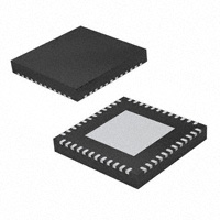


 工商网监
湘ICP备2023018690号
工商网监
湘ICP备2023018690号
