AIC111
www.ti.com
SLAS382A – JUNE 2003 – REVISED NOVEMBER 2005
IC DESIGN SPECIFICATION
1.3-V microPower™ DSP/μC VOICE BAND AUDIO CODEC
Check for Samples: AIC111
FEATURES
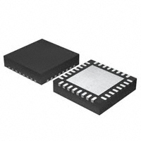
– - 32-Pin QFN 5×5-mm Plastic Package
– - 32-Pad Bumped Die in Waffle Pack (wafer
scale packaging)
1
•
•
2
•
•
•
•
•
•
•
•
•
•
•
•
Single Channel Codec
Noise Shaped Delta Sigma ADC and DAC
Technology
Low Supply Voltage and Current:
– 1.3-V Typical Power Supply
– 350-µA Typical Supply Current Drain
Power Supply Up Monitor and Low Battery
Monitor That Also Automatically Shuts Off HBridge Output When Battery Decays Below
1.05 V in a Nontransient Manner
Typical 2.4-µVrms Input Referred Noise With
0.01% Total Harmonic Distortion for Front End
and 108-dB Dynamic Range
ADC Has 87-dB Dynamic Range With 73-dB
Total Harmonic Distortion 100 Hz-10 kHz, 40kHz Sampling Rate
Typical 55-dB PSRR 100 Hz to 10 kHz for
Analog Front End
Low Noise Programmable Gain
Amplifier/Compressor Front End With
Programmable Fast and Slow Attack and
Decay Rates With Dual or Single Attack and
Decay Rate Option
Typical Output Noise of 12 µVrms With 0.05%
Total Harmonic Distortion for Delta Sigma DAC
and H-Bridge Output Driver
Low Jitter Oscillator That Generates all
Internal Clocks and Generates 5-MHz Output
DSP/µC Clock
Regulated Bandgap Voltage Reference
Programmable Functionality via Digital Serial
Interface
– McBSP Interface, DSP Protocol
– TI TMS320VC54x™, TMS320VC55x™ DSPs
– SPI Interface, Microcontroller Protocol
– TI MSP430xx
External Chip Power Down and Reset
Available in:
APPLICATIONS
•
•
•
•
•
Hearing Instruments
Personal Medical Devices
Hearing Protection
Aural Processing
Low-Power Headsets
DESCRIPTION
The AIC111 IC design specification serves to provide
product development teams with a guideline for how
the AIC111 IC is specified and programmable options
that are available. The document outlines a top-level
block description of the IC along with system
specifications and functions. Individual block
descriptions and target specifications are also
outlined.
The Texas Instruments AIC111 is a TI µPower DSP
compatible, or microcontroller compatible audio
codec product, or analog interface circuit. The
AIC111 is part of a comprehensive family of DSP/µC
based high-performance analog interface solutions.
The AIC111 is targeted primarily at personal medical
devices, such as hearing instruments, aural
preprocessing applications, and low-power headset
applications. The AIC111 is used in any design
requiring
a
programmable
time
constant
PGA/compressor interface, high dynamic range
analog-to-digital converter, an external DSP/µC
handling signal processing, or a low distortion digitalto-analog converter with a balanced H-Bridge
speaker driver. It supports a CMOS digital interface
tailored for TI DSPs with the McBSP protocol such as
TMS320VC54x™ DSP family and SPI-based
controllers such as TI MSP430x family of
microcontrollers. The AIC111 also has an external
microphone or sensor supply and bias and power
supply up low-battery monitor indicator.
1
2
Please be aware that an important notice concerning availability, standard warranty, and use in critical applications of
Texas Instruments semiconductor products and disclaimers thereto appears at the end of this data sheet.
microPower is a trademark of Texas Instruments.
UNLESS OTHERWISE NOTED this document contains
PRODUCTION DATA information current as of publication date.
Products conform to specifications per the terms of Texas
Instruments standard warranty. Production processing does not
necessarily include testing of all parameters.
Copyright © 2003–2005, Texas Instruments Incorporated
�AIC111
SLAS382A – JUNE 2003 – REVISED NOVEMBER 2005
www.ti.com
These devices have limited built-in ESD protection. The leads should be shorted together or the device placed in conductive foam during
storage or handling to prevent electrostatic damage to the MOS gates.
This integrated circuit can be damaged by ESD. Texas Instruments recommends that all integrated circuits be handled with
appropriate precautions. Failure to observe proper handling and installation procedures can cause damage.
ESD damage can range from subtle performance degradation to complete device failure. Precision integrated circuits may be more
susceptible to damage because very small parametric changes could cause the device not to meet its published specifications.
The AIC111 comes in a 32-pin QFN 5×5-mm package. A 32-pad solder ball bumped flip chip die that comes in
waffle packs or tape and reel is in preview and will be available 3rd quarter 2003.
AVAILABLE OPTIONS (1)
Part Number
Package
AIC111RHB
32-pin QFN (5 mm x 5 mm), in tube.
AIC111RHBR
32-pin QFN (5 mm x 5 mm), tape and reel
AIC111YE
32-pad waffle scale chip package, bumped die in waffle pack (commercial)
AIC111YE
32-pad waffle scale chip package, bumped die in waffle pack (industrial)
AIC111YER
(1)
32-pad (WSCP) bumped die in tape and reel
For the most current package and ordering information, see the Package Option Addendum at the end of this document, or see the TI
website at www.ti.com.
ABSOLUTE MAXIMUM RATINGS
over operating free-air temperature range unless otherwise noted( (1))( (2))
UNIT
TA
Input voltage
AI or DI pins
Power supply
VDD, power pins
Latch-up tolerance
JEDEC latch-up (EIA/JEDS78)
Operating free-air temperature range,
-0.3 V to 4 V
-0.3 V to 4.5 V
100 mA
Commerical
0°C to 70°C
−40°C to 85°C
Industrial
Functional temperature range
Tstg
-15°C to 85°C
Reflow temperature range (flip chip)
220°C to 230°C
Storage temperature range
-40°C to 125°C
Storage humidity
(1)
(2)
65% R.H.
Stresses beyond those listed under absolute maximum ratings may cause permanent damage to the device. These are stress ratings
only, and functional operation of the device at these or any other conditions beyond those indicated under recommended operating
conditions is not implied. Exposure to absolute-maximum-rated conditions for extended periods may affect device reliability.
Specifications are assured operating at maximum device limits for QFN package only, unless otherwise specified.
ELECTRICAL CHARACTERISTICS
INPUT/OUTPUT, OPERATING TEMPERATURE AT 25°C
PARAMETER
Digital interface (see
(1)
and
TEST CONDITION
(2)
)
BUF_DVDD (see Note
MIN
TYP
(1)
)
MAX
UNIT
3.6
V
VIH
High-level input voltage
BUF_DVDD0.2
VIL
Low-level input voltage
BUF_DVSS+
0.2
V
VOH
High-level output voltage
BUF_DVDD
V
VOL
Low-level output voltage
BUF_DVSS
V
Maximum allowed input voltage (AVIN)
(1)
(2)
2
Differential
V
450 mVpk
DVDD, VDD_OSC, and AVDD should be within 50 mV, preferably connected together. AVSS1, 2, DVSS, and VSS_OSC should be
within 50 mV, preferably connected together.
Maximum (0.9 V, DVDD -0.5 V) ≤ BUF_DVDD ≤3.6 V
Copyright © 2003–2005, Texas Instruments Incorporated
�AIC111
www.ti.com
SLAS382A – JUNE 2003 – REVISED NOVEMBER 2005
ELECTRICAL CHARACTERISTICS (continued)
INPUT/OUTPUT, OPERATING TEMPERATURE AT 25°C
PARAMETER
Input impedance (AVIN) (see
TEST CONDITION
(3)
)
MIN
Nominal gain = 50x
Input capacitance (AVIN)
Microphone bias voltage (MIC_VSUP)
20-μA maximum
Microphone bias resistor (MIC_BIAS)
(3)
H-bridge amplifier output
DAC full scale output
differential
Output resistance
Differential, HB - VDD = 1.3 V
TYP
MAX
UNIT
20
kΩ
5
pF
0.87
0.94
0.99
V
27
29.1
31
kΩ
Fixed Q
3/4 HB_VDD
Adaptive Q
HB_VDD
20 or 40
VPP
Ω
Driving single-ended: Rin = R × [(1+A)/(2+A)], A = PGAC Gain (linear), R = 20.4 kΩ for A ≥4 or 20.4 kΩ× (4/A) for A
很抱歉,暂时无法提供与“AIC111RHBG4”相匹配的价格&库存,您可以联系我们找货
免费人工找货