AIC111
www.ti.com
SLAS382 – JUNE 2003
IC DESIGN SPECIFICATION
1.3-V microPower DSP/µC VOICE BAND AUDIO CODEC
FEATURES
D Single Channel Codec
D Noise Shaped Delta Sigma ADC and DAC
Technology
D Low Supply Voltage and Current:
– 1.3-V Typical Power Supply
– 350-µA Typical Supply Current Drain
D Power Supply Up Monitor and Low Battery
Monitor That Also Automatically Shuts Off
H-Bridge Output When Battery Decays Below
1.05 V in a Nontransient Manner
D Typical 2.4-µVrms Input Referred Noise With
0.01% Total Harmonic Distortion for Front
End and 108-dB Dynamic Range
D ADC Has 87-dB Dynamic Range With 73-dB
Total Harmonic Distortion 100 Hz–10 kHz,
40-kHz Sampling Rate
D Typical 55-dB PSRR 100 Hz to 10 kHz for
Analog Front End
D Low Noise Programmable Gain
Amplifier/Compressor Front End With
Programmable Fast and Slow Attack and
Decay Rates With Dual or Single Attack and
Decay Rate Option
D Typical Output Noise of 12 µVrms With 0.05%
Total Harmonic Distortion for Delta Sigma
DAC and H-Bridge Output Driver
D Low Jitter Oscillator That Generates all
Internal Clocks and Generates 5-MHz Output
DSP/µC Clock
D Regulated Bandgap Voltage Reference
D Programmable Functionality via Digital Serial
Interface
– McBSP Interface, DSP Protocol
– TI TMS320VC54x, TMS320VC55x DSPs
– SPI Interface, Microcontroller Protocol
– TI MSP430xx
D External Chip Power Down and Reset
D Available in:
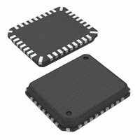
– 32-Pin QFN 5×5-mm Plastic Package
– 32-Pad Bumped Die in Waffle Pack (wafer
scale packaging), or Tape and Reel,
(Preview, Available 3rd Quarter 2003)
APPLICATIONS
D Hearing Instruments
D Personal Medical Devices
D Hearing Protection
D Aural Processing
D Low-Power Headsets
DESCRIPTION
The AIC111 IC design specification serves to provide
product development teams with a guideline for how the
AIC111 IC is specified and programmable options that are
available. The document outlines a top-level block
description of the IC along with system specifications and
functions. Individual block descriptions and target
specifications are also outlined.
The Texas Instruments AIC111 is a TI µPower DSP
compatible, or microcontroller compatible audio codec
product, or analog interface circuit. The AIC111 is part of
a comprehensive family of DSP/µC based highperformance analog interface solutions. The AIC111 is
targeted primarily at personal medical devices, such as
hearing instruments, aural preprocessing applications,
and low-power headset applications. The AIC111 is used
in any design requiring a programmable time constant
PGA/compressor interface,
high
dynamic range
analog-to-digital converter, an external
DSP/µC
handling signal processing, or a low distortion
digital-to-analog converter with a balanced H-Bridge
speaker driver. It supports a CMOS digital interface
tailored for TI DSPs with the McBSP protocol such as
TMS320VC54x DSP family and SPI-based controllers
such as TI MSP430x family of microcontrollers. The
AIC111 also has an external microphone or sensor supply
and bias and power supply up low-battery monitor
indicator.
Please be aware that an important notice concerning availability, standard warranty, and use in critical applications of Texas Instruments
semiconductor products and disclaimers thereto appears at the end of this data sheet.
This document contains information on products in more than one phase of
development. The status of each device is indicated on the page(s) specifying its
electrical characteristics.
Copyright 2003, Texas Instruments Incorporated
�AIC111
www.ti.com
SLAS382 – JUNE 2003
These devices have limited built-in ESD protection. The leads should be shorted together or the device placed in conductive foam during
storage or handling to prevent electrostatic damage to the MOS gates.
The AIC111 comes in a 32-pin QFN 5×5-mm package. A 32-pad solder ball bumped flip chip die that comes in waffle
packs or tape and reel is in preview and will be available 3rd quarter 2003.
AVAILABLE OPTIONS
PART NUMBER
PACKAGE
AIC111RHB
32-pin QFN (5 mm x 5 mm), in tube.
AIC111RHBR
32-pin QFN (5 mm x 5 mm), tape and reel
AIC111YE
32-pad waffle scale chip package, bumped die in waffle pack (contact the factory for availability) – Preview,
available 3rd quarter 2003
AIC111YER
32-pad (WSCP) bumped die in tape and reel (contact the factory for availability) – Preview, available 3rd
quarter 2003
ABSOLUTE MAXIMUM RATINGS
over operating free-air temperature range unless otherwise noted(1)(2)
UNIT
Input voltage
AI or DI pins
–0.3 V to 4 V
Power supply
VDD, power pins
Latch-up tolerance
JEDEC latch-up (EIA/JEDS78)
–0.3 V to 4.5 V
100 mA
Operating free-air temperature range, TA
0°C to 70°C
Functional temperature range
–15°C to 85°C
Reflow temperature range (flip chip)
220°C to 230°C
Storage temperature range, Tstg
–40°C to 125°C
Storage humidity
65% R.H.
(1) Stresses beyond those listed under absolute maximum ratings may cause permanent damage to the device. These are stress ratings only, and
functionaloperation of the device at these or any other conditions beyond those indicated under recommendedoperating conditions is not implied.
Exposure to absolute-maximum-rated conditions for extended periods may affect device reliability.
(2) Specifications are assured operating at maximum device limits for QFN package only, unless otherwise specified.
ELECTRICAL CHARACTERISTICS
INPUT/OUTPUT, OPERATING TEMPERATURE AT 25°C
PARAMETER
Digital interface (see Notes 1 and 2)
TEST CONDITION
MIN
VOH High-level output voltage
VOL Low-level output voltage
Differential
Input impedance (AVIN) (see Note 3)
Nominal gain = 50x
V
V
BUF_DVDD
V
V
20
0.87
Microphone bias resistor (MIC_BIAS)
27
Fixed Q
DAC full scale output differential
Adaptive Q
mVpk
kΩ
5
20-µA maximum
V
BUF_DVSS+0.2
450
Input capacitance (AVIN)
UNIT
BUF_DVDD–0.2
BUF_DVSS
Maximum allowed input voltage (AVIN)
H bridge amplifier output
H-bridge
MAX
3.6
VIH High-level input voltage
VIL Low-level input voltage
Microphone bias voltage (MIC_VSUP)
TYP
BUF_DVDD (see Note 1)
pF
0.94
0.99
29.1
31
V
kΩ
3/4 HB_VDD
HB_VDD
VPP
Output resistance
Differential, HB – VDD = 1.3 V
20 or 40
Ω
(1) DVDD, VDD_OSC, and AVDD should be within 50 mV, preferably connected together.
AVSS1, 2, DVSS, and VSS_OSC should be within 50 mV, preferably connected together.
(2) Maximum (0.9 V, DVDD –0.5 V) ≤ BUF_DVDD ≤3.6 V
(3) Driving single-ended: Rin = R × [(1+A)/(2+A)], A = PGAC Gain (linear), R = 20.4 kΩ for A ≥ 4 or 20.4 kΩ × (4/A) for A 1.1 V
100
ms
Allowed transient spike below 1.05 V before H-bridge output and digital interface
are not asserted.
VDD < 1.05 V
44
µs
POR on
1.1
POR off
1.05
V
11
�AIC111
www.ti.com
SLAS382 – JUNE 2003
DIGITAL INTERFACE
Function: The digital interface can be selected (IMODE=LOW) as a serial audio/control interface (SACI), which is
the McBSP DSP-codec protocol, or (IMODE=HIGH), a serial peripheral interface (SPI). Either SACI or SPI sends
out a 16-bit audio stream from the ∆–Σ ADC and receives a 20-bit audio stream going to the ∆–Σ DAC/H-Bridge.
Several control functions, READ/WRITE to user registers, are also included totaling five 8-bit registers. Four pins,
SCLK, FRAME, SDIN and SDOUT, are employed in SACI or SPI. An internal register map exists that contains
read/write program registers for a variety of FORMAT (user) settings. The register bits that are designated not used
will always read back zero or voltage level VSS regardless of what is written to them.
DIG INTERFACE PIN
I/O
DESCRIPTION
SCLK
Output
Bit shift clock. SCLK has an internal pull down.
FRAME
Output
Data frame sync: controls the separation of audio channels and provides a reset/synchronization
to the interface’s internal state machine. FRAME has an internal pull down.
SDIN
Input
Serial audio/control data input pin.
SDOUT
Input
Serial audio/control data output pin.
IMODE
Input
Interface protocol selection pin. LOW=SACI, HIGH=SPI.
MCLK
Output
Clock output pin.
SLAVE
MASTER
SDOUT
DR
FRAME
FSX
FSR
AIC111
SDIN
DX
SCLK
CLKR
CLKS
CLKX
MCLK
C54x
CLKIN
(See Note A)
NOTE A:
The dotted line indicates the connection is not essential for communication to work.
Figure 5. AIC111 McBSP DSP-Codec Interface
McBSP DSP-Codec (SACI) Protocol
Use this protocol when interfacing to TI DSPs.
D The SACI works in a master mode.
D SCLK = 1.28 MHz. FRAME (= 40 kHz) has a 50% duty cycle. FRAME is an output.
D 32-bit control/audio data, written on the SDIN pin, consist of a 20-bit audio word going to the ∆–Σ DAC, and a
12-bit control word.
D DAC input has two modes of operation, a 20-bit mode, and a 16-bit mode.
D The 12-bit control word consists of: a R/W bit, 3 address bits, and 8-bits of control register content. Note that
the R/W bit is defined as 0=READ, and 1=WRITE.
D When the 3 address bits are all zeros, the control function of the SACI is disabled.
D 24-bit audio/control data, read from the SDOUT pin, consist of one 16-bit output from the ∆–Σ ADC followed by
an 8-bit control word.
D All data/control words are formatted as the MSB first.
12
�AIC111
www.ti.com
SLAS382 – JUNE 2003
20-Bit Mode
D/A Input
D19 – D0
AIC111 Input
D19 – D0
16-Bit Mode
D19 – D0
D/A Input
AIC111 Input
D19 D19 D19 D19
D19 – D4
D19 D19 D19
D19 – D4
0
Shift = 1
D19 D19
D19 – D4
0 0
Shift = 2
D19
D19 – D4
0 0 0
Shift = 3
D19 – D4
0 0 0 0
Shift = 4
D18 – D4
0 0 0 0 0
Shift = 0
Shift = 5
See Note B
NOTE B:
For 5-bit left shift, digital word is limited to 15 bits with sataration.
Figure 6. AIC111 Data Output
13
�AIC111
SLAS382 – JUNE 2003
14
Figure 7. AIC111 DSP-Codec (SACI) Signals (Read = 0, Write = 1)
FRAME
SCLK
1
SDIN
SDOUT
2
3
4
5
6
7
8
9
10
11
12
13
14
D19 D18 D17 D16 D15 D14 D13 D12 D11 D10 D9
D8 D7 D6
D15 D14 D13 D12 D11 D10 D9
D4 D3
D8
D7 D6
D5
15
16
D5 D4
D2 D1
D0
17
18
D3 D2
19
20
21
22
23
24
25
26
27
28
29
30
31
32
D1 D0 W/R A2 A1
A0
C7
C6 C5 C4
C3 C2
C1 C0 D19 D18
C7
C6 C5 C4
C3 C2
C1 C0 D15 D14
www.ti.com
�AIC111
www.ti.com
SLAS382 – JUNE 2003
SLAVE
GPIO
MASTER
AIC111
FRAME
STE
SDOUT
SIMO
SDIN
SOMI
SCLK
UCLK
MCLK
MCLK
MSP430x
Figure 8. AIC111 SPI I/O Diagram
SPI Protocol
D AIC111 can also implement a master SPI protocol.
D SCLK supplies a bit shift clock of 1.28 MHz to the SPI port of a slave device.
D FRAME must be in the active low state prior to data transaction and must stay low for the duration of data
transaction. Before communication, there are eight silent cycles on SCLK. During this period FRAME also sends
a pulse to reset the slave device.
D When the control function is not required, the AIC111 transmits a 16-bit audio word to and receives a 20-bit audio
word from the slave device in every FRAME cycle.
D A WRITE/READ of an 8-bit user register (address 0x01 to 0x07) takes two FRAME cycles.
D All data/control words are formatted as the MSB first.
15
�AIC111
www.ti.com
D0
D3 D2 D1
D4
D8
D7 D6 D5
D15 D14 D13 D12 D11 D10 D9
D4
D7 D6 D5
D8
D19 D18 D17 D16 D15 D14 D13 D12 D11 D10 D9
Don’t Care
SDOUT
SDIN
SCLK
FRAME
31
32
1
2
3
4
5
6
7
8
9
10
11
12
13
14
15
16
17
18
19
20
21
22
23
24
25
26
D3 D2 D1
27
28
29
D0 W/R A2
30
A1
31
A0
32
SLAS382 – JUNE 2003
NOTE: If A2, A1, and A0 = 0, one gets audio data only and W/R is a don’t care. If in the previous frame A2, A1, and A0 = 0, then one gets both audio
and control data depending on the W/R bit defined as Read = 0 and Write = 1.
Figure 9. AIC111 SPI Signals
16
�SDOUT
SDIN
SCLK
FRAME
31
32
1
2
3
5
Don’t Care
4
6
7
8
13
14
15
16
17
18
19
20
D8
D7 D6 D5
D4
12
D15 D14 D13 D12 D11 D10 D9
11
D8
10
D19 D18 D17 D16 D15 D14 D13 D12 D11 D10 D9
9
D0
24
D3 D2 D1
23
D4
22
D7 D6 D5
21
26
27
C7 C6
C5
C7 C6 C5
25
30
31
C0
32
C1 C0
C3 C2 C1
29
C4 C3 C2
C4
28
www.ti.com
SLAS382 – JUNE 2003
AIC111
NOTE: SDIN shows writing to A2, A1, and A0 specified from the previous frame. SDOUT shows reading from A2, A1, and A0 specified from a
different previous frame.
Figure 10. AIC111 SPI Signals
17
�AIC111
www.ti.com
SLAS382 – JUNE 2003
Digital Interface Timing
PARAMETER
F_sclk
SCLK frequency
F_frame
FRAME frequency
MIN
TYP
MAX
1.28
MHz
F-sclk/32
MHz
Digital Interface Block Diagram
PGA/Compressor
ADC
SCLK
FRAME
DAC/H–Bridge
SDIN
CONTROL REGISTERS
McBSP/SPI
CONTROL LOGIC
SDOUT
DATA BLOCK
Oscillator
IMODE
MCLK
Power–on Reset
Mic Power/VREF
Register Map and Register Bit Definitions
ADDRESS
REGISTER NAME
0x00
Reserved
0x01
PGACREG
0x02
HPFSFTREG
HPF and shift control register
0x03
PDCREG
Power-down control register
0x04
FASTARREG
Fast attack/release rate control register
0x05
SLOWARREG
Slow attack/release rate control register
0x06–07
Reserved
NOTE: Do not write to the reserved registers.
18
DETAILED DESCRIPTION
Reserved for future use
PGAC gain register
Reserved for future use
UNIT
�AIC111
www.ti.com
SLAS382 – JUNE 2003
PGACREG
BIT
NAME
7
PGAC_READ_MODE
Select register contents or actual gain to read
0: Read FORMAT0 register contents (default)
1: Read actual PGAC gain
PGAC_GAIN [6:0]
PGAC gain adjustment (0.5 dB steps). A full table is found in the
Appendix Section of this data sheet.
0x52 = +40.0 dB
0x51 = +39.5 dB
0x50 = +39.0 dB
…
0x46 =+34.0 dB (default)
….
0x01 = –0.5 dB
0x00 = –1.0 dB
6:0
FUNCTION
DEFAULT=0x46
HPFSFTREG
BIT
7
NAME
FUNCTION
DBUFF_EN
Enable weak (1/2 strength) dig I/O buffer
6:5
HPF_CTL [1:0]
Control bits for high-pass filter
00: normal mode
01: HPF bypass
10: 100 Hz corner frequency
11: Not used
4:2
SHIFT [2:0]
Select shift bits when ADC 16-b output is used as DAC 20-b input.
000: no shift
–24 db gain
001: 1b left shift
–18 dB gain
010: 2b left shift
–12 dB gain
011: 3b left shift
–6 dB gain
100: 4b left shift (default) 0 dB gain
101: 5b left shift
+6 dB gain
11X: 5b left shift
1:0
DAC_MODE
Select DAC mode of operation.
00: DAC off, powered down
01: 16-bit input goes through shifter (default)
10: 20-bit input bypasses shifter
11: ADC→DAC digital loopback
DEFAULT=0x11
PDCREG
BIT
NAME
FUNCTION
7
DAC_ADAPTIVE_Q
0 = fixed quantization, 1 = adaptive quantization
6
HB_OUT_EN
H-bridge output enable
5
HB_DRIVE
H-bridge drive strength, 0 = 40 Ω, 1 = 20 Ω
4
HIST_TIMEOUT_SEL
PGAC hysteresis timeout select
0: 50 ms (default)
1: 25 ms
3:2
PGAC_GAIN_MODE
Set gain mode of PGAC
00: Automatic, dual rate (default)
01: Automatic, single rate
10: Fixed, single rate
11: Fixed, immediate
1
MIC_VSUP_PD
Power down MIC_VSUP
0
FRONTEND_PD
Power down PGAC+ADC
DEFAULT=0x00
19
�AIC111
www.ti.com
SLAS382 – JUNE 2003
FASTARREG PGAC Fast Rates
BIT
NAME
7:4
ATTACK
FUNCTION
1111: Attack rate = 80000 dB/s
1110: Attack rate = 40000 dB/s
1101: Attack rate = 20000 dB/s
1100: Attack rate = 10000 dB/s
1011: Attack rate = 5000 dB/s
1010: Attack rate = 2500 dB/s
1001: Attack rate = 1250 dB/s
1000: Attack rate = 625 dB/s
0111: Attack rate = 312.5 dB/s
0110: Attack rate = 156.25 dB/s
0101: Attack rate = 78.13 dB/s
0100: Attack rate = 39.1 dB/s
0011: Attack rate = 19.53 dB/s
0010: Attack rate = 9.77 dB/s
0001: Attack rate = 4.88 dB/s
0000: Attack rate = 2.44 dB/s
3:0
RELEASE
1111: Release rate = 80000 dB/s
1110: Release rate = 40000 dB/s
…
0001: Release rate = 4.88 dB/s
0000: Release rate = 2.44 dB/s
DEFAULT=0xF7
SLOWARREG PGAC Slow Rates (Dual Rate Mode Only)
20
BIT
NAME
FUNCTION
7:4
ATTACK
1111: Attack rate = 80000 dB/s
1110: Attack rate = 40000 dB/s
…
0001: Attack rate = 4.88 dB/s
0000: Attack rate = 2.44 dB/s
3:0
RELEASE
1111: Release rate = 80000 dB/s
1110: Release rate = 40000 dB/s
…
0001: Release rate = 4.88 dB/s
0000: Release rate = 2.44 dB/s
DEFAULT=0x42
�AIC111
www.ti.com
SLAS382 – JUNE 2003
APPENDIX
PGAC GAIN
PGAC GAIN VALUES
PGAC
PGAC
BUS NAME
HEX VALUE
BINARY
PGAC_GAIN
_
0x52
1010010
40
0x51
1010001
39.5
0x50
1010000
39
0x4F
1001111
38.5
PGAC_GAIN
_
GAIN (DB)
0x4E
1001110
38
0x4D
1001101
37.5
0x4C
1001100
37
0x4B
1001011
36.5
0x4A
1001010
36
0x49
1001001
35.5
0x48
1001000
35
0x47
1000111
34.5
0x46
1000110
34
0x45
1000101
33.5
0x44
1000100
33
0x43
1000011
32.5
0x42
1000010
32
0x41
1000001
31.5
0x40
1000000
31
30.5
0x3F
0111111
0x3E
0111110
30
0x3D
0111101
29.5
0x3C
0111100
29
0x3B
0111011
28.5
0x3A
0111010
28
0x39
0111001
27.5
0x38
0111000
27
0x37
0110111
26.5
0x36
0110110
26
0x35
0110101
25.5
0x34
0110100
25
0x33
0110011
24.5
0x32
0110010
24
0x31
0110001
23.5
0x30
0110000
23
22.5
0x2F
0101111
0x2E
0101110
22
0x2D
0101101
21.5
0x2C
0101100
21
0x2B
0101011
20.5
0x2A
0101010
20
0x29
0101001
19.5
0x28
0101000
19
0x27
0100111
18.5
0x26
0100110
18
0x25
0100101
17.5
0x24
0100100
17
0x23
0100011
16.5
21
�AIC111
www.ti.com
SLAS382 – JUNE 2003
PGAC GAIN VALUES
PGAC ((Continued))
PGAC
BUS NAME
HEX VALUE
BINARY
PGAC_GAIN
_
0x22
0100010
16
0x21
0100001
15.5
0x20
0100000
15
0x1F
0011111
14.5
PGAC_GAIN
_
Default
22
GAIN (DB)
0x1E
0011110
14
0x1D
0011101
13.5
0x1C
0011100
13
0x1B
0011011
12.5
0x1A
0011010
12
0x19
0011001
11.5
0x18
0011000
11
0x17
0010111
10.5
0x16
0010110
10
0x15
0010101
9.5
0x14
0010100
9
0x13
0010011
8.5
0x12
0010010
8
0x11
0010001
7.5
0x10
0010000
7
0x0F
0001111
6.5
0x0E
0001110
6
0x0D
0001101
5.5
0x0C
0001100
5
0x0B
0001011
4.5
0x0A
0001010
4
0x09
0001001
3.5
0x08
0001000
3
0x07
0000111
2.5
0x06
0000110
2
0x05
0000101
1.5
0x04
0000100
1
0x03
0000011
0.5
0x02
0000010
0
0x01
0000001
–0.5
0x00
0000000
–1
�AIC111
www.ti.com
SLAS382 – JUNE 2003
VCC
ZINC AIR
BATTERY
1.3V
VSS
BUF_DVDD
AVDD
DVDD
TI TMS320C54xx APPLICATION CIRCUIT
MIC_VSUP
SCLK
MIC_BIAS
CLKR
CLKS
CLKX
SDIN
DX
Microphone
AIC111
B
U
F
F
E
R
S
1.3V
H
B
R
I
D
G
E
HB_VDD
HB_VSS
Speaker
I/O
SDOUT
DR
M
c
B
S
P
’C54x
FRAME
FSX
FSR
RST/LBM
MCLK
RST
CLKIN
BUF_DVSS
DVSS
AVSS
EXT_RST/PWDN
LBM = Low Battery Monitor
Figure 11. Interfacing to the TMS320C54xx for a Hearing Aid Application
Required external capacitors:
D
D
D
D
D
1-µF coupling capacitor on AVINP, AVINM
1-µF from VMID_FILT to analog ground
1-µF from VREF to analog ground
0.1-µF from MIC_VSUP to analog ground
At least 0.1-µF from VRFILT to analog ground. 1-µF from VRFILT to analog ground is recommended.
23
�AIC111
www.ti.com
SLAS382 – JUNE 2003
2.8 V
VCC
VSS
DVDD
AVDD
1.3 V
BUF_DVDD
TI MSP430F12x APPLICATION CIRCUIT
P2.5
(See Note A)
MIC_VSUP
MIC_BIAS
Microphone
SCLK
INCLK
SDIN
SOMI
SDOUT
SIMO
FRAME
STE
MSP430F12x
I/O
AIC111
Speaker
B
U
F
F
E
R
S
RST/LBM
XIN
BUF_DVSS
DVSS
AVSS
MCLK
RST/NMI
LBM = Low Battery Monitor ’430 Can Also Use
EXT_RST/PWDN to Reset or Power Down the AIC111
Note A: P2.5 enables the MSP430F12x to shut down the AIC111 when desired.
Figure 12. Interfacing to the MSP430F12x for a Hearing Aid Application
24
�AIC111
www.ti.com
SLAS382 – JUNE 2003
MECHANICAL AND ENVIRONMENTAL
Packaging
The AIC111 is available in a 32-pin quad QFN 5x5-mm package. The AIC111 will be available 3rd quarter 2003 as
bare solder ball bumped die intended for direct PCB mounting (also known as wafer scale packaging).
D
D
D
D
For QFN packaged part in tubes order: AIC111RHB.
For QFN packaged part in tape and reel order: AIC111RHBR.
For ball bumped die (in waffle pack) order: AIC111YE (Preview, available 3rd quarter 2003).
For ball bumped die (in tape and reel) order: AIC111YER (Preview, available 3rd quarter 2003).
BOND PAD PITCH AND DIE AREA
X = 2737.62 µ, Y = 3175.02 µ,
(107.78 mil, 125.0 mil)
(2,74 mm, 3,18 mm)
13.47kmil2 (8.69mm2)
Die dimensions
Maximum die area (includes scribe area)
202.95 µ or 7.99 mil
Minimum bond pad pitch
Nearest
PAD (#)
7
30
12
14
16
28
18
20
21
22
25
9
10
23
1
32
4
27
17
6
2
3
PITCH
PAD (#)
8
31
13
15
15
29
19
19
20
21
26
10
11
24
32
1
5
28
16
7
1
2
(micron)
(mil)
202.950
202.950
237.690
237.690
237.690
241.200
256.410
256.410
256.410
256.410
287.651
295.470
295.470
306.360
327.147
327.147
356.940
357.034
359.453
369.450
371.520
380.700
(7.990)
(7.990)
(9.358)
(9.358)
(9.358)
(9.496)
(10.095)
(10.095)
(10.095)
(10.095)
(11.325)
(11.633)
(11.633)
(12.061)
(12.880)
(12.880)
(14.053)
(14.056)
(14.152)
(14.545)
(14.627)
(14.988)
25
�AIC111
www.ti.com
SLAS382 – JUNE 2003
Number of pins
32
Pad locations:
Bond Pad Coordinates
Units: microns
Dimensions:
X = 2737.62 Y = 3175
Bond pad origin: X = 0.000
Y = 0.000
Bond pad offset: X = 0.000
Y = 0.000
(X,Y) = (0,0) is located at the left bottom of the die by pads 8 and 9.
See section 1.6, Figure 1–1.
Bond Pad Dimensions
Pad #
Xcenter
Ycenter
Diameter
1
2
3
4
5
6
7
8
9
10
11
12
13
14
15
16
17
18
19
20
21
22
23
24
25
26
27
28
29
30
31
32
154.080
154.080
154.080
154.080
154.080
154.080
154.080
154.080
410.310
705.780
1001.250
1327.860
1565.550
1803.240
2040.930
2278.620
2574.990
2574.990
2574.990
2574.990
2574.990
2574.990
2574.990
2574.990
2574.990
2371.590
1910.430
1553.850
1312.650
955.530
752.580
410.310
2808.990
2437.470
2056.770
1676.070
1319.130
938.430
568.980
366.030
162.630
162.630
162.630
162.630
162.630
162.630
162.630
162.630
366.030
782.550
1038.960
1295.370
1551.780
1808.190
2188.890
2495.250
2808.990
3012.390
2994.390
3012.390
3012.390
3012.390
3012.390
3012.390
70.020
70.020
70.020
70.020
70.020
70.020
70.020
70.020
70.020
70.020
70.020
70.020
70.020
70.020
70.020
70.020
70.020
70.020
70.020
70.020
70.020
70.020
70.020
70.020
70.020
70.020
70.020
70.020
70.020
70.020
70.020
70.020
DIE THICKNESS
Final die thickness Z (without solder bump)
TYPICAL
TOLERANCE
29.59 mil or 725 µm
±0.79 mil or 20 µm
SOLDER BUMP
D Bump metal composition: 37% Pb (lead)/63% Sn (tin)
D Type: Spherical
BUMP SPEC.
Bump height
Re-flow temperature
TYPICAL
TOLERANCE
100 µm
+8 µm
NOTE
Tolerance across a single die.
+16 µm
Tolerance across any wafer.
183°C
WAFFLE SCALE PACKAGE DISCLAIMERS FOR AIC11YE AND AIC11YER
D The AIC111’s die bond pads, their peripheral placement, passivation opening, and layout are in accordance with
ASE’s Bumping Design Guide revision D, June, 2001.
D The final application is assumed to use plastic overmolding where the die is hermetically sealed, and the
maximum ratings apply only to the QFN package and not to the WSCP.
26
��IMPORTANT NOTICE
Texas Instruments Incorporated and its subsidiaries (TI) reserve the right to make corrections, modifications,
enhancements, improvements, and other changes to its products and services at any time and to discontinue
any product or service without notice. Customers should obtain the latest relevant information before placing
orders and should verify that such information is current and complete. All products are sold subject to TI’s terms
and conditions of sale supplied at the time of order acknowledgment.
TI warrants performance of its hardware products to the specifications applicable at the time of sale in
accordance with TI’s standard warranty. Testing and other quality control techniques are used to the extent TI
deems necessary to support this warranty. Except where mandated by government requirements, testing of all
parameters of each product is not necessarily performed.
TI assumes no liability for applications assistance or customer product design. Customers are responsible for
their products and applications using TI components. To minimize the risks associated with customer products
and applications, customers should provide adequate design and operating safeguards.
TI does not warrant or represent that any license, either express or implied, is granted under any TI patent right,
copyright, mask work right, or other TI intellectual property right relating to any combination, machine, or process
in which TI products or services are used. Information published by TI regarding third-party products or services
does not constitute a license from TI to use such products or services or a warranty or endorsement thereof.
Use of such information may require a license from a third party under the patents or other intellectual property
of the third party, or a license from TI under the patents or other intellectual property of TI.
Reproduction of information in TI data books or data sheets is permissible only if reproduction is without
alteration and is accompanied by all associated warranties, conditions, limitations, and notices. Reproduction
of this information with alteration is an unfair and deceptive business practice. TI is not responsible or liable for
such altered documentation.
Resale of TI products or services with statements different from or beyond the parameters stated by TI for that
product or service voids all express and any implied warranties for the associated TI product or service and
is an unfair and deceptive business practice. TI is not responsible or liable for any such statements.
Following are URLs where you can obtain information on other Texas Instruments products and application
solutions:
Products
Applications
Amplifiers
amplifier.ti.com
Audio
www.ti.com/audio
Data Converters
dataconverter.ti.com
Automotive
www.ti.com/automotive
DSP
dsp.ti.com
Broadband
www.ti.com/broadband
Interface
interface.ti.com
Digital Control
www.ti.com/digitalcontrol
Logic
logic.ti.com
Military
www.ti.com/military
Power Mgmt
power.ti.com
Optical Networking
www.ti.com/opticalnetwork
Microcontrollers
microcontroller.ti.com
Security
www.ti.com/security
Telephony
www.ti.com/telephony
Video & Imaging
www.ti.com/video
Wireless
www.ti.com/wireless
Mailing Address:
Texas Instruments
Post Office Box 655303 Dallas, Texas 75265
Copyright 2004, Texas Instruments Incorporated
�