BQ2022A
SLUS724F – SEPTEMBER 2006 – REVISED JANUARY 2022
BQ2022A 1-Kbit Serial EPROM with SDQ Interface
1 Features
3 Description
•
The BQ2022A is a 1-Kbit serial EPROM containing
a factory-programmed, unique 48-bit identification
number, 8-bit CRC generation, and the 8-bit family
code (09h). A 64-bit status register controls write
protection and page redirection.
•
•
•
•
•
•
1024 bits of one-time programmable (OTP)
EPROM for storage of user-programmable
configuration data
Factory-programmed unique 64-bit identification
number
Single-wire interface to reduce circuit board routing
Synchronous communication reduces host
interrupt overhead
15-KV IEC 61000-4-2 ESD compliance on data pin
No standby power required
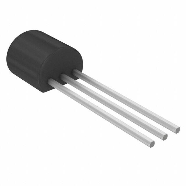
Available in a 3-pin SOT-23 package and TO-92
package
2 Applications
•
•
•
•
Security encoding
Inventory tracking
Product-revision maintenance
Battery-pack identification
The BQ2022A SDQ™ interface requires only a single
connection and a ground return. The DATA pin is also
the sole power source for the BQ2022A.
The small surface-mount package options saves
printed-circuit-board space, while the low cost makes
it ideal for applications such as battery pack
configuration parameters, record maintenance, asset
tracking, product-revision status, and access-code
security.
Device Information
PART NUMBER
BQ2022A
(1)
PACKAGE(1)
BODY SIZE (NOM)
SOT-23 (3)
2.92 mm × 1.30 mm
TO-92 (3)
4.30 mm × 4.30 mm
For all available packages, see the orderable addendum at
the end of the data sheet.
SPACER
SPACER
SDQ
VSS
1
SDQ Communications
Controller and 8-Bit CRC
Generation Circuit
Internal
Bus
EPROM
MEMORY
(1024 bits)
2
bq2022A
ID ROM
(64 bits)
RAM
Buffer
(8 bytes)
EPROM
STATUS
(64 bits)
3
VSS
Simplified Schematic
An IMPORTANT NOTICE at the end of this data sheet addresses availability, warranty, changes, use in safety-critical applications,
intellectual property matters and other important disclaimers. PRODUCTION DATA.
�BQ2022A
www.ti.com
SLUS724F – SEPTEMBER 2006 – REVISED JANUARY 2022
Table of Contents
1 Features............................................................................1
2 Applications..................................................................... 1
3 Description.......................................................................1
4 Revision History.............................................................. 2
5 Pin Configuration and Functions...................................3
6 Specifications.................................................................. 3
6.1 Absolute Maximum Ratings........................................ 3
6.2 ESD Ratings............................................................... 3
6.3 Recommended Operating Conditions.........................3
6.4 Thermal Information....................................................4
6.5 Electrical Characteristics: DC..................................... 4
6.6 Switching Characteristics: AC.....................................4
6.7 Typical Characteristics................................................ 5
7 Detailed Description........................................................5
7.1 Overview..................................................................... 5
7.2 Functional Block Diagram........................................... 6
7.3 Feature Description.....................................................6
7.4 Device Functional Modes............................................8
7.5 Programming.............................................................. 8
8 Application and Implementation.................................. 17
8.1 Application Information............................................. 17
8.2 Typical Application.................................................... 17
9 Power Supply Recommendations................................19
10 Layout...........................................................................19
10.1 Layout Guidelines................................................... 19
10.2 Layout Example...................................................... 20
11 Device and Documentation Support..........................21
11.1 Third-Party Products Disclaimer............................. 21
11.2 Documentation Support.......................................... 21
11.3 Trademarks............................................................. 21
11.4 Support Resources................................................. 21
11.5 Electrostatic Discharge Caution.............................. 21
11.6 Glossary.................................................................. 21
12 Mechanical, Packaging, and Orderable
Information.................................................................... 21
4 Revision History
NOTE: Page numbers for previous revisions may differ from page numbers in the current version.
Changes from Revision E (March 2016) to Revision F (January 2022)
Page
• Updated Pin Configuration and Functions ......................................................................................................... 3
Changes from Revision D (December 2014) to Revision E (February 2016)
Page
• Added text: "No additional capacitance..." to Section 8.2 ................................................................................17
• Added Section 8.2.2.2 ..................................................................................................................................... 18
• Added text and Figure 9-1 to Section 9 ........................................................................................................... 19
2
Submit Document Feedback
Copyright © 2022 Texas Instruments Incorporated
Product Folder Links: BQ2022A
�BQ2022A
www.ti.com
SLUS724F – SEPTEMBER 2006 – REVISED JANUARY 2022
5 Pin Configuration and Functions
SDQ
1
3
VSS
VSS
2
Figure 5-1. DBZ Package 3-Pin SOT-23 (Top View)
1
VSS
2
SDQ
3
NC
Figure 5-2. LP Package 3-Pin TO-92 (Bottom View)
Table 5-1. Pin Functions
PIN
TYPE
DESCRIPTION
NAME
SOT-23
TO-92
SDQ
1
2
I
VSS
2, 3
1
—
Ground. Both pins should be connected to system ground.
NC
—
3
—
No connection. This pin should be connected to system ground or left floating.
Data
6 Specifications
6.1 Absolute Maximum Ratings
over operating free-air temperature range (unless otherwise noted) (1)
MIN
MAX
UNIT
–0.3
7
V
Low-level output current, IOL
40
mA
ESD IEC 61000-4-2 air discharge, data to VSS, VSS to data
15
kV
DC voltage applied to data, VPU
Operating free-air temperature, TA
–20
70
°C
Communication free-air temperature, TA(Comm) (2)
–40
85
°C
125
°C
125
°C
Junction temperature, TJ
Storage temperature, Tstg
(1)
(2)
–55
Operation outside the Absolute Maximum Ratings may cause permanent device damage. Absolute Maximum Ratings do not imply
functional operation of the device at these or any other conditions beyond those listed under Recommended Operating Conditions. If
outside the Recommended Operating Conditions but within the Absolute Maximum Ratings, the device may not be fully functional, and
this may affect device reliability, functionality, performance, and shorten the device lifetime.
Communication is specified by design.
6.2 ESD Ratings
VALUE
Human body model (HBM), per ANSI/ESDA/JEDEC
V(ESD)
(1)
(2)
Electrostatic discharge
JS-001(1)
UNIT
±2000
Charged device model (CDM), per JEDEC specification JESD22C101(2)
V
±500
JEDEC document JEP155 states that 500-V HBM allows safe manufacturing with a standard ESD control process.
JEDEC document JEP157 states that 250-V CDM allows safe manufacturing with a standard ESD control process.
6.3 Recommended Operating Conditions
over operating free-air temperature range (unless otherwise noted)
MIN
VPU
Operational pullup voltage
2.65
NOM
MAX
5.5
UNIT
V
Submit Document Feedback
Copyright © 2022 Texas Instruments Incorporated
Product Folder Links: BQ2022A
3
�BQ2022A
www.ti.com
SLUS724F – SEPTEMBER 2006 – REVISED JANUARY 2022
6.3 Recommended Operating Conditions (continued)
over operating free-air temperature range (unless otherwise noted)
MIN
RPU
NOM
Serial communication interface pullup resistance
MAX
5
UNIT
kΩ
6.4 Thermal Information
BQ2022A
THERMAL METRIC(1)
DBZ (3 PINS)
LP (3 PINS)
RθJA
Junction-to-ambient thermal resistance
244.3
158.5
RθJC(top)
Junction-to-case (top) thermal resistance
104.9
55.6
RθJB
Junction-to-board thermal resistance
93.1
n/a
ψJT
Junction-to-top characterization parameter
4.8
26.8
ψJB
Junction-to-board characterization parameter
66.4
137.8
RθJC(bot)
Junction-to-case (bottom) thermal resistance
n/a
n/a
(1)
UNIT
°C/W
For more information about traditional and new thermal metrics, see the IC Package Thermal Metrics Application Report (SPRA953).
6.5 Electrical Characteristics: DC
TA = –20°C to 70°C; VPU(min) = 2.65 VDC to 5.5 VDC, all voltages relative to VSS
PARAMETER
TEST CONDITIONS
MIN
TYP
MAX
UNIT
IDATA
Supply current
VPU = 5.5 V
20
μA
VOL
Low-level output voltage
Logic 0, VPU = 5.5 V, IOL = 4 mA, SDQ pin
0.4
V
VOH
High-level output voltage
Logic 1
IOL
Low-level output current (sink)
VOL = 0.4 V, SDQ pin
VIL
Low-level input voltage
Logic 0
VIH
High-level input voltage
Logic 1
VPP
Programming voltage
Logic 0, VPU = 2.65 V, IOL = 2 mA
0.4
VPU
5.5
4
0.8
2.2
mA
V
V
11.5
12
V
6.6 Switching Characteristics: AC
TA = –20°C to 70°C; VPU(min) = 2.65 VDC to 5.5 VDC, all voltages relative to VSS
PARAMETER
MIN
MAX
UNIT
60
120
μs
1
15
μs
(1)
tWSTRB
15
μs
(1)(2)
60
tc
μs
tc
Bit cycle time
tWSTRB
Write start cycle
(1)
tWDSU
Write data setup
tWDH
Write data hold
trec
TEST CONDITIONS
(1)
Recovery time
(1)
1
For memory command only
4
(1)
tRSTRB
Read start cycle
tODD
Output data delay
tODHO
Output data hold
tRST
Reset time
(1)
(1)
(1)
μs
5
1
13
μs
tRSTRB
13
μs
17
60
μs
480
(1)
μs
tPPD
Presence pulse delay
tPP
Presence pulse
tEPROG
EPROM programming time
2500
μs
tPSU
Program setup time
5
μs
tPREC
Program recovery time
5
μs
(1)
Submit Document Feedback
15
60
μs
60
240
μs
Copyright © 2022 Texas Instruments Incorporated
Product Folder Links: BQ2022A
�BQ2022A
www.ti.com
SLUS724F – SEPTEMBER 2006 – REVISED JANUARY 2022
6.6 Switching Characteristics: AC (continued)
TA = –20°C to 70°C; VPU(min) = 2.65 VDC to 5.5 VDC, all voltages relative to VSS
PARAMETER
tPRE
Program rising-edge time
tPFE
Program falling-edge time
TEST CONDITIONS
MIN
tRSTREC
(1)
(2)
MAX
UNIT
5
μs
5
μs
480
μs
5-kΩ series resistor between SDQ pin and VPU. (See Figure 8-1.)
tWDH must be less than tc to account for recovery.
6.7 Typical Characteristics
2.3
0.1
VOL - Low-level Output Voltage (V)
IDATA - Supply Current (PA)
2.2
2.1
2
1.9
1.8
1.7
1.6
VPU = 2.5V
VPU = 3.0V
VPU =5.0V
1.5
1.4
-40
-20
0
20
40
Temperature (°C)
60
80
D001
0.06
0.04
0.02
-20
0
20
40
Temperature (°C)
60
80
100
D002
Figure 6-2. Low-Level Output Voltage vs
Temperature
2.4
1.4
VPU = 2.5V
VPU = 3V
VPU = 5.5V
1.2
VIH - High-level Input Voltage (V)
VIL - Low-level Input Voltage (V)
0.08
0
-40
100
Figure 6-1. Supply Current vs Temperature
1
0.8
0.6
0.4
-40
VPU = 5.5V
IOL = 4mA
-20
0
20
40
Temperature (°C)
60
80
100
2.2
2
1.8
1.6
1.4
-40
D003
Figure 6-3. Low-Level Input Voltage vs
Temperature
-20
0
20
40
Temperature (°C)
60
80
100
D004
Figure 6-4. High-Level Input Voltage vs
Temperature
7 Detailed Description
7.1 Overview
Section 7.2 shows the relationships among the major control and memory sections of the BQ2022A. The
BQ2022A has three main data components: a 64-bit factory-programmed ROM, including 8-bit family code,
48-bit identification number and 8-bit CRC value, 1024-bit EPROM, and EPROM STATUS bytes. Power for read
and write operations is derived from the DATA pin. An internal capacitor stores energy while the signal line
is high and releases energy during the low times of the DATA pin, until the pin returns high to replenish the
charge on the capacitor. A special manufacturer's PROGRAM PROFILE BYTE can be read to determine the
programming profile required to program the part.
Submit Document Feedback
Copyright © 2022 Texas Instruments Incorporated
Product Folder Links: BQ2022A
5
�BQ2022A
www.ti.com
SLUS724F – SEPTEMBER 2006 – REVISED JANUARY 2022
7.2 Functional Block Diagram
SDQ
VSS
1
SDQ Communications
Controller and 8-Bit CRC
Generation Circuit
Internal
Bus
EPROM
MEMORY
(1024 bits)
2
bq2022A
ID ROM
(64 bits)
RAM
Buffer
(8 bytes)
EPROM
STATUS
(64 bits)
3
VSS
7.3 Feature Description
7.3.1 1024-Bit EPROM
Table 7-1 is a memory map of the 1024-bit EPROM section of the BQ2022A, configured as four pages of 32
bytes each. The 8-byte RAM buffers are additional registers used when programming the memory. Data are first
written to the RAM buffer and then verified by reading an 8-bit CRC from the BQ2022A that confirms proper
receipt of the data. If the buffer contents are correct, a programming command is issued and an 8-byte segment
of data is written into the selected address in memory. This process ensures data integrity when programming
the memory. The details for reading and programming the 1024-bit EPROM portion of the BQ2022A are in
Section 7.5.4 section of this data sheet.
Table 7-1. 1024-Bit EPROM Data Memory Map
6
ADDRESS(HEX)
PAGE
0060-007F
Page 3
0040-005F
Page 2
0020-003F
Page 1
0000-001F
Page 0
Submit Document Feedback
Copyright © 2022 Texas Instruments Incorporated
Product Folder Links: BQ2022A
�BQ2022A
www.ti.com
SLUS724F – SEPTEMBER 2006 – REVISED JANUARY 2022
7.3.2 EPROM Status Memory
In addition to the programmable 1024-bits of memory are 64 bits of status information contained in the EPROM
STATUS memory. The STATUS memory is accessible with separate commands. The STATUS bits are EPROM
and are read or programmed to indicate various conditions to the software interrogating the BQ2022A. The first
byte of the STATUS memory contains the write protect page bits, that inhibit programming of the corresponding
page in the 1024-bit main memory area if the appropriate write-protection bit is programmed. Once a bit has
been programmed in the write protect page byte, the entire 32-byte page that corresponds to that bit can no
longer be altered but may still be read. The write protect bits may be cleared by using the WRITE STATUS
command.
The next four bytes of the EPROM STATUS memory contain the page address redirection bytes. Bits in
the EPROM status bytes can indicate to the host what page is substituted for the page by the appropriate
redirection byte. The hardware of the BQ2022A makes no decisions based on the contents of the page address
redirection bytes. This feature allows the user's software to make a data patch to the EPROM by indicating that
a particular page or pages should be replaced with those indicated in the page address redirection bytes. The
ones complement of the new page address is written into the page address redirection byte that corresponds to
the original (replaced) page. If a page address redirection byte has an FFh value, the data in the main memory
that corresponds to that page are valid. If a page address redirection byte has some other hex value, the data
in the page corresponding to that redirection byte are invalid, and the valid data can now be found at the ones
complement of the page address indicated by the hexadecimal value stored in the associated page address
redirection byte. A value of FDh in the redirection byte for page 1, for example, indicates that the updated data
are now in page 2. The details for reading and programming the EPROM status memory portion of the BQ2022A
are given in Section 7.5.4 section.
Table 7-2. EPROM Status Bytes
ADDRESS (HEX)
PAGE
00h
Write protection bits
BIT0—write protect page 0
BIT1—write protect page 1
BIT2—write protect page 2
BIT3—write protect page 3
BIT4 to 7—bitmap of used pages
01h
Redirection byte for page 0
02h
Redirection byte for page 1
03h
Redirection byte for page 2
04h
Redirection byte for page 3
05h
Reserved
06h
Reserved
07h
Factory programmed 00h
7.3.3 Error Checking
To validate the data transmitted from the BQ2022A, the host generates a CRC value from the data as they are
received. This generated value is compared to the CRC value transmitted by the BQ2022A. If the two CRC
values match, the transmission is error-free. The equivalent polynomial function of this CRC is X8 + X5 + X4 + 1.
Section 7.5.16 provides details.
7.3.4 Customizing the BQ2022A
The 64-bit ID identifies each BQ2022A. The 48-bit serial number is unique and programmed by Texas
Instruments. The default 8-bit family code is 09h; however, a different value can be reserved on an individual
customer basis. Contact your Texas Instruments sales representative for more information.
7.3.5 Bus Termination
Because the drive output of the BQ2022A is an open-drain, N-channel MOSFET, the host must provide a source
current or a 5-kΩ external pullup, as shown in the typical application circuit in Figure 8-1.
Submit Document Feedback
Copyright © 2022 Texas Instruments Incorporated
Product Folder Links: BQ2022A
7
�BQ2022A
www.ti.com
SLUS724F – SEPTEMBER 2006 – REVISED JANUARY 2022
7.4 Device Functional Modes
The device is in active mode during SDQ communication or while the SDQ is kept at valid VPU voltages.
7.5 Programming
7.5.1 Serial Communication
A host reads, programs, or checks the status of the BQ2022A through the command structure of the SDQ
interface.
7.5.2 Initialization
Initialization consists of two pulses, the RESET and the PRESENCE pulses. The host generates the RESET
pulse, while the BQ2022A responds with the PRESENCE pulse. The host resets the BQ2022A by driving the
DATA bus low for at least 480 μs. For more details, see Section 7.5.11.
7.5.3 ROM Commands
7.5.3.1 READ ROM Command
The READ ROM command sequence is the fastest sequence that allows the host to read the 8-bit family code
and 48-bit identification number. The READ ROM sequence starts with the host generating the RESET pulse
of at least 480 μs. The BQ2022A responds with a PRESENCE pulse. Next, the host continues by issuing the
READ ROM command, 33h, and then reads the ROM and CRC byte using the READ signaling (see the READ
and WRITE signals section) during the data frame.
Reset
and
Presence
Signals
1
1
Read ROM (33h)
0
0
1
1
0
Family Code and Identification
Number (7 BYTES)
0
CRC (1 BYTE)
Figure 7-1. READ ROM Sequence
7.5.3.2 SKIP ROM Command
This SKIP ROM command, CCh, allows the host to access the memory/status functions. The SKIP ROM
command is directly followed by a memory/status functions command.
Reset
and
Presence
Signals
Skip ROM (CCh)
0
1
0
1
0
1
0
1
Figure 7-2. SKIP ROM Sequence
7.5.4 Memory/Status Function Commands
Six memory/status function commands allow read and modification of the 1024-bit EPROM data memory or the
64-bit EPROM status memory. There are two types of READ MEMORY command, plus the WRITE MEMORY,
READ STATUS, and WRITE STATUS commands. Additionally, the part responds to a PROGRAM PROFILE
byte command. The BQ2022A responds to memory/status function commands only after a part is issued a SKIP
ROM command.
7.5.5 READ MEMORY Commands
Two READ MEMORY commands are available on the BQ2022A. Both commands are used to read data from
the 1024-bit EPROM data field. They are the READ MEMORY/Page CRC and the READ MEMORY/Field CRC
commands. The READ MEMORY/Page CRC generates CRC at the end any 32-byte page boundary whereas
the READ MEMORY/Field CRC generates CRC when the end of the 1024-bit data memory is reached.
8
Submit Document Feedback
Copyright © 2022 Texas Instruments Incorporated
Product Folder Links: BQ2022A
�BQ2022A
www.ti.com
SLUS724F – SEPTEMBER 2006 – REVISED JANUARY 2022
7.5.5.1 READ MEMORY/Page CRC
To read memory and generate the CRC at the 32-byte page boundaries of the BQ2022A, the SKIP ROM
command is followed by the READ MEMORY/Generate CRC command, C3h, followed by the address low byte
and then the address high byte.
An 8-bit CRC of the command byte and address bytes is computed by the BQ2022A and read back by the host
to confirm that the correct command word and starting address were received. If the CRC read by the host is
incorrect, a reset pulse must be issued and the entire sequence must be repeated. If the CRC received by the
host is correct, the host issues read time slots and receives data from the BQ2022A starting at the initial address
and continuing until the end of a 32-byte page is reached. At that point, the host sends eight additional read time
slots and receive an 8-bit CRC that is the result of shifting into the CRC generator all of the data bytes from the
initial starting byte to the last byte of the current page. Once the 8-bit CRC has been received, data is again read
from the 1024-bit EPROM data field starting at the next page. This sequence continues until the final page and
its accompanying CRC are read by the host. Thus each page of data can be considered to be 33 bytes long,
the 32 bytes of user-programmed EPROM data and an 8-bit CRC that gets generated automatically at the end of
each page.
Figure 7-3. READ MEMORY/Page CRC
Initialization and SKIP
ROM Command
Sequence
READ MEMORY/
Generate CRC
Command
C3h
Address Low Byte
A0
Address High
Byte
A7 A8
A15
Read and
Verify CRC
EPROM Memory and CRC
Byte
Generated at 32-Byte
Page
Boundaries
NOTE: Individual bytes of address and data are transmitted LSB first.
7.5.5.2 READ MEMORY/Field CRC
To read memory without CRC generation on 32-byte page boundaries, the SKIP ROM command is followed by
the READ MEMORY command, F0h, followed by the address low byte and then the address high byte.
Note
As shown in Figure 7-4, individual bytes of address and data are transmitted LSB first.
An 8-bit CRC of the command byte and address bytes is computed by the BQ2022A and read back by the host
to confirm that the correct command word and starting address were received. If the CRC read by the host is
incorrect, a reset pulse must be issued and the entire sequence must be repeated. If the CRC received by the
host is correct, the host issues read time slots and receives data from the BQ2022A starting at the initial address
and continuing until the end of the 1024-bit data field is reached or until a reset pulse is issued. If reading
occurs through the end of memory space, the host may issue eight additional read time slots and the BQ2022A
responds with an 8-bit CRC of all data bytes read from the initial starting byte through the last byte of memory.
After the CRC is received by the host, any subsequent read time slots appear as logical 1s until a reset pulse
is issued. Any reads ended by a reset pulse prior to reaching the end of memory does not have the 8-bit CRC
available.
Submit Document Feedback
Copyright © 2022 Texas Instruments Incorporated
Product Folder Links: BQ2022A
9
�BQ2022A
www.ti.com
SLUS724F – SEPTEMBER 2006 – REVISED JANUARY 2022
Figure 7-4. READ MEMORY/Field CRC
Initialization and SKIP
ROM Command
Sequence
READ MEMORY Command
F0h
Address Low
Byte
A0
Address High
Byte
A7 A8
Read and
Verify
CRC
Read EPROM
Memory Until
End of EPROM
Memory
Read and
Verify CRC
A15
7.5.6 WRITE MEMORY Command
The WRITE MEMORY command is used to program the 1024-bit EPROM memory field. The 1024-bit memory
field is programmed in 8-byte segments. Data is first written into an 8-byte RAM buffer one byte at a time. The
contents of the RAM buffer is then ANDed with the contents of the EPROM memory field when the programming
command is issued.
Figure 7-5 illustrates the sequence of events for programming the EPROM memory field. After issuing a SKIP
ROM command, the host issues the WRITE MEMORY command, 0Fh, followed by the low byte and then the
high byte of the starting address. The BQ2022A calculates and transmits an 8-bit CRC based on the WRITE
command and address.
If at any time during the WRITE MEMORY process, the CRC read by the host is incorrect, a reset pulse must be
issued, and the entire sequence must be repeated.
After the BQ2022A transmits the CRC, the host then transmits 8 bytes of data to the BQ2022A. Another 8-bit
CRC is calculated and transmitted based on the 8 bytes of data. If this CRC agrees with the CRC calculated
by the host, the host transmits the program command 5Ah and then applies the programming voltage for at
least 2500 μs or tEPROG. The contents of the RAM buffer is then logically ANDed with the contents of the 8-byte
EPROM offset by the starting address.
The starting address can be any integer multiple of eight between 0000 and 007F (hex) such as 0000, 0008, and
0010 (hex).
The WRITE DATA MEMORY command sequence can be terminated at any point by issuing a reset pulse except
during the program pulse period tPROG.
Note
The BQ2022A responds with the data from the selected EPROM address sent least significant-bit first.
This response should be checked to verify the programmed byte. If the programmed byte is incorrect,
then the host must reset the part and begin the write sequence again.
For both of these cases, the decision to continue programming is made entirely by the host, because the
BQ2022A is not able to determine if the 8-bit CRC calculated by the host agrees with the 8-bit CRC calculated
by the BQ2022A.
Prior to programming, bits in the 1024-bit EPROM data field appear as logical 1 s.
10
Submit Document Feedback
Copyright © 2022 Texas Instruments Incorporated
Product Folder Links: BQ2022A
�BQ2022A
www.ti.com
SLUS724F – SEPTEMBER 2006 – REVISED JANUARY 2022
Write Memory
Command?
(0Fh)
Selected
State
N
Selected
State
Y
Bus Master Transmits Low Byte Address
(LSB First) AD0 to AD7
Bus Master Transmits High Byte Address
(LSB First) AD8 to AD15
bq2022A
Loads Address Into Address Counter
bq2022A Transmits CRC of Write Command
and Address, then Clears CRC Register
bq2022A Receives 8 Bytes of Data and
Stores in RAM Buffer
bq2022A Transmits
CRC of Previous Received 8 Bytes of Data
N
Code 5Ah
Received
Y
Voltage on Data
Pin = VPP
N
Y
Contents of RAM buffer AND’ed with contents of
data memory offset by
address counter and stored in data
memory offset by address counter .
programming time required to be at
least t EPROG when VPP Vdc on data pin
bq2022A
Increments Address
Counter and Transmits 1
Byte of Data Memory
Indexed by Address Counter
bq2022A
8th Byte
Transmitted
Transmits 1 Byte of Data Memory
at Address Counter
N
Y
bq2022A Waits for Reset
(No Further Response)
NOTE: Individual bytes of address and data are transmitted LSB first
Figure 7-5. WRITE MEMORY Command Flow
7.5.7 READ STATUS Command
The READ STATUS command is used to read data from the EPROM status data field. After issuing a SKIP ROM
command, the host issues the READ STATUS command, AAh, followed by the address low byte and then the
address high byte.
Submit Document Feedback
Copyright © 2022 Texas Instruments Incorporated
Product Folder Links: BQ2022A
11
�BQ2022A
www.ti.com
SLUS724F – SEPTEMBER 2006 – REVISED JANUARY 2022
Note
An 8-bit CRC of the command byte and address bytes is computed by the BQ2022A and read back by
the host to confirm that the correct command word and starting address were received.
If the CRC read by the host is incorrect, a reset pulse must be issued and the entire sequence must be repeated.
If the CRC received by the host is correct, the host issues read time slots and receives data from the BQ2022A
starting at the supplied address and continuing until the end of the EPROM Status data field is reached. At that
point, the host receives an 8-bit CRC that is the result of shifting into the CRC generator all of the data bytes
from the initial starting byte through the final factory-programmed byte that contains the 00h value.
This feature is provided because the EPROM status information may change over time making it impossible
to program the data once and include an accompanying CRC that is always valid. Therefore, the READ status
command supplies an 8-bit CRC that is based on (and always is consistent with) the current data stored in the
EPROM status data field.
After the 8-bit CRC is read, the host receives logical 1s from the BQ2022A until a reset pulse is issued. The
READ STATUS command sequence can be ended at any point by issuing a reset pulse.
Figure 7-6. READ STATUS Command
Initialization and SKIP
ROM Command
Sequence
READ MEMORY Command
AAh
Address Low
Byte
A0
Address High Read and
Byte
Verify CRC
A7 A8
Read STATUS
Memory Until
End of STATUS
Memory
Read and
Verify CRC
A15
7.5.8 WRITE STATUS Command
The WRITE STATUS command is used to program the EPROM Status data field after the BQ2022A has been
issued SKIP ROM command.
The flow chart in Figure 7-7 illustrates that the host issues the WRITE STATUS command, 55h, followed by the
address low byte and then the address high byte the followed by the byte of data to be programmed.
Note
Individual bytes of address and data are transmitted LSB first. An 8-bit CRC of the command byte,
address bytes, and data byte is computed by the BQ2022A and read back by the host to confirm that
the correct command word, starting address, and data byte were received.
If the CRC read by the host is incorrect, a reset pulse must be issued and the entire sequence must be repeated.
If the CRC received by the host is correct, the program command (5Ah) is issued. After the program command is
issued, then the programming voltage, VPP is applied to the DATA pin for period tPROG. Prior to programming, the
first seven bytes of the EPROM STATUS data field appear as logical 1s. For each bit in the data byte provided
by the host that is set to a logical 0, the corresponding bit in the selected byte of the EPROM STATUS data field
is programmed to a logical 0 after the programming pulse has been applied at the byte location. The eighth byte
of the EPROM STATUS byte data field is factory-programmed to contain 00h.
12
Submit Document Feedback
Copyright © 2022 Texas Instruments Incorporated
Product Folder Links: BQ2022A
�BQ2022A
www.ti.com
SLUS724F – SEPTEMBER 2006 – REVISED JANUARY 2022
Write Status
Command?
(55h)
Selected
State
N
Selected
State
Y
bq2022A Receives Low Address Byte
(LSB First) AD0 to AD7
bq2022A Receives High Address Byte
(LSB First) AD8 to AD15
bq2022A Loads Address into Address Counter
bq2022A Receives 1 Byte of Data
and Stores in RAM Buffer
bq2022A Transmits CRC of Write Status
Command, Address, and Data
bq2022A
Calculates and Transmits
CRC of Loaded Address and
Shifted Data
N
Code 5Ah
Received
Y
VDATA = VPP?
N
Y
Contents of RAM buffer AND’ed with contents of
data memory as pointed to by address counter .
Programming time required to be at least
t EPROG when VPP is applied to the data pin
bq2022A
Receives Data Byte
bq2022A
Increments Address
Counter and Loads
New Address into CRC
Register
bq2022A
Transmits Data Byte of
Status Memory Pointed
to by Address Counter
End of Status
Memory?
N
Y
bq2022A Waits for Reset
Figure 7-7. WRITE STATUS Command Flow
After the programming pulse is applied and the data line returns to VPU, the host issues eight read time slots
to verify that the appropriate bits have been programmed. The BQ2022A responds with the data from the
selected EPROM STATUS address sent least significant bit first. This response should be checked to verify the
programmed byte. If the programmed byte is incorrect, then the host must reset the device and begin the write
Submit Document Feedback
Copyright © 2022 Texas Instruments Incorporated
Product Folder Links: BQ2022A
13
�BQ2022A
www.ti.com
SLUS724F – SEPTEMBER 2006 – REVISED JANUARY 2022
sequence again. If the BQ2022A EPROM data byte programming was successful, the BQ2022A automatically
increments its address counter to select the next byte in the STATUS MEMORY data field. The least significant
byte of the new two-byte address is also loaded into the 8-bit CRC generator as a starting value. The host issues
the next byte of data using eight write time slots.
As the BQ2022A receives this byte of data into the RAM buffer, it also shifts the data into the CRC generator
that has been preloaded with the LSB of the current address and the result is an 8-bit CRC of the new data byte
and the LSB of the new address. After supplying the data byte, the host reads this 8-bit CRC from the BQ2022A
with eight read time slots to confirm that the address incremented properly and the data byte was received
correctly. If the CRC is incorrect, a Reset Pulse must be issued and the Write Status command sequence must
be restarted. If the CRC is correct, the host issues a programming pulse and the selected byte in memory is
programmed.
Note
The initial write of the WRITE STATUS command, generates an 8-bit CRC value that is the result of
shifting the command byte into the CRC generator, followed by the two-address bytes, and finally the
data byte. Subsequent writes within this WRITE STATUS command due to the BQ2022A automatically
incrementing its address counter generates an 8-bit CRC that is the result of loading (not shifting) the
LSB of the new (incremented) address into the CRC generator and then shifting in the new data byte.
For both of these cases, the decision to continue programming the EPROM Status registers is made entirely
by the host, because the BQ2022A is not able to determine if the 8-bit CRC calculated by the host agrees with
the 8-bit CRC calculated by the BQ2022A. If an incorrect CRC is ignored and a program pulse is applied by the
host, incorrect programming could occur within the BQ2022A. Also note that the BQ2022A always increments
its internal address counter after the receipt of the eight read time slots used to confirm the programming of
the selected EPROM byte. The decision to continue is again made entirely by the host, therefore if the EPROM
data byte does not match the supplied data byte but the master continues with the WRITE STATUS command,
incorrect programming could occur within the BQ2022A. The WRITE STATUS command sequence can be
ended at any point by issuing a reset pulse.
Table 7-3. Command Code Summary
COMMAND
(HEX)
DESCRIPTION
CATEGORY
33h
Read Serialization ROM and
CRC
ROM Commands Available in Command Level I
CCh
Skip Serialization ROM
F0h
Read Memory/Field CRC
AAh
Read EPROM Status
C3h
Read Memory/Page CRC
0Fh
Write Memory
99h
Programming Profile
55h
Write EPROM Status
5Ah
Program Control
Memory Function Commands
Available in Command Level II
Program Command Available Only in WRITE
MEMORY and WRITE STATUS Modes
7.5.9 PROGRAM PROFILE Byte
The PROGRAM PROFILE byte is read to determine the WRITE MEMORY programming sequence required
by a specific manufacturer. After issuing a ROM command, the host issues the PROGRAM PROFILE BYTE
command, 99h. Figure 7-8 shows the BQ2022A responds with 55h. This informs the host that the WRITE
MEMORY programming sequence is the one described in Section 7.5.6.
14
Submit Document Feedback
Copyright © 2022 Texas Instruments Incorporated
Product Folder Links: BQ2022A
�BQ2022A
www.ti.com
SLUS724F – SEPTEMBER 2006 – REVISED JANUARY 2022
From SKIP
ROM
Command
Program
Profile Command?
99h
N
Other
Command
Codes
Y
bq2022 Transmits
55h
bq2022A
is in
Reset State
Master Issues Reset
Figure 7-8. PROGRAM PROFILE Command Flow
7.5.10 SDQ Signaling
All SDQ signaling begins with initializing the device, followed by the host driving the bus low to write a 1 or 0, or
to begin the start frame for a bit read. Figure 7-9 shows the initialization timing, whereas Figure 7-10 and Figure
7-11 show that the host initiates each bit by driving the DATA bus low for the start period, tWSTRB / tRSTRB. After
the bit is initiated, either the host continues controlling the bus during a WRITE, or the BQ2022A responds during
a READ.
7.5.11 RESET and PRESENCE PULSE
If the DATA bus is driven low for more than 120 μs, the BQ2022A may be reset. Figure 7-9 shows that if the
DATA bus is driven low for more than 480 μs, the BQ2022A resets and indicates that it is ready by responding
with a PRESENCE PULSE.
VPU
VIH
VIL
RESET
(Sent by Host)
Presence Pulse
(Sent by bq2022A)
t PPD
t RST
t PP
t RSTREC
Figure 7-9. Reset Timing Diagram
7.5.12 WRITE Bit
The WRITE bit timing diagram in Figure 7-10 shows that the host initiates the transmission by issuing the tWSTRB
portion of the bit and then either driving the DATA bus low for a WRITE 0, or releasing the DATA bus for a
WRITE 1.
Write ”1”
V PU
V IH
V IL
Write ”0”
t rec
t WSTRB
t WDSU
t WDH
Figure 7-10. WRITE Bit Timing Diagram
Submit Document Feedback
Copyright © 2022 Texas Instruments Incorporated
Product Folder Links: BQ2022A
15
�BQ2022A
www.ti.com
SLUS724F – SEPTEMBER 2006 – REVISED JANUARY 2022
7.5.13 READ Bit
The READ bit timing diagram in Figure 7-11 shows that the host initiates the transmission of the bit by issuing
the tRSTRB portion of the bit. The BQ2022A then responds by either driving the DATA bus low to transmit a READ
0 or releasing the DATA bus to transmit a READ 1.
Read ”1”
VPU
V IH
V IL
Read ”0”
t RSTRB
t REC
t ODD
t ODHO
Figure 7-11. READ Bit Timing Diagram
7.5.14 PROGRAM PULSE
VPP
VPU
tPSU
tPFE
tPRE
tPREC
tEPROG
VSS
Figure 7-12. PROGRAM PULSE Timing Diagram
7.5.15 IDLE
If the bus is high, the bus is in the IDLE state. Bus transactions can be suspended by leaving the DATA bus in
IDLE. Bus transactions can resume at any time from the IDLE state.
7.5.16 CRC Generation
The BQ2022A has an 8-bit CRC stored in the most significant byte of the 64-bit ROM. The bus master can
compute a CRC value from the first 56 bits of the 64-bit ROM and compare it to the value stored within
the BQ2022A to determine if the ROM data has been received error-free by the bus master. The equivalent
polynomial function of this CRC is: X8 + X5 + X4 +1.
Under certain conditions, the BQ2022A also generates an 8-bit CRC value using the same polynomial function
just shown and provides this value to the bus master to validate the transfer of command, address, and data
bytes from the bus master to the BQ2022A. The BQ2022A computes an 8-bit CRC for the command, address,
and data bytes received for the WRITE MEMORY and the WRITE STATUS commands and then outputs this
value to the bus master to confirm proper transfer. Similarly, the BQ2022A computes an 8-bit CRC for the
command and address bytes received from the bus master for the READ MEMORY, READ STATUS, and READ
DATA/ GENERATE 8-BIT CRC commands to confirm that these bytes have been received correctly. The CRC
generator on the BQ2022A is also used to provide verification of error-free data transfer as each page of data
from the 1024-bit EPROM is sent to the bus master during a READ DATA/GENERATE 8-BIT CRC command,
and for the eight bytes of information in the status memory field.
In each case where a CRC is used for data transfer validation, the bus master must calculate a CRC value
using the polynomial function previously given and compare the calculated value to either the 8-bit CRC value
stored in the 64-bit ROM portion of the BQ2022A (for ROM reads) or the 8-bit CRC value computed within the
BQ2022A. The comparison of CRC values and decision to continue with an operation are determined entirely by
the bus master. No circuitry on the BQ2022A prevents a command sequence from proceeding if the CRC stored
in or calculated by the BQ2022A does not match the value generated by the bus master. Proper use of the CRC
can result in a communication channel with a high level of integrity.
16
Submit Document Feedback
Copyright © 2022 Texas Instruments Incorporated
Product Folder Links: BQ2022A
�BQ2022A
www.ti.com
SLUS724F – SEPTEMBER 2006 – REVISED JANUARY 2022
CLK
DAT
Q
D
R
Q
D
Q
R
D
Q
R
D
+
R
Q
D
+
Q
R
D
Q
R
D
R
Q
D
+
R
UDG-02065
Figure 7-13. 8-Bit CRC Generator Circuit (X8 + X5 + X4 + 1)
8 Application and Implementation
Note
Information in the following applications sections is not part of the TI component specification,
and TI does not warrant its accuracy or completeness. TI’s customers are responsible for
determining suitability of components for their purposes, as well as validating and testing their design
implementation to confirm system functionality.
8.1 Application Information
A typical application consists of a microcontroller that is configured to be a SDQ communication host device and
the BQ2022A being the SDQ slave device. The host and slave have open drain functionality for which a pullup
resistor (typically 10 kΩ) is required connected to a pullup voltage in the range of 2.65 V to 5.5 V.
8.2 Typical Application
No additional capacitance is needed on the SDQ line and may result in a communication failure.
VPU
bq2022 A
SDQ
SDQI
1
Communications
Controller
CPU
SDQO
VSS
2
VSS
3
HOST
Figure 8-1. Typical Application Circuit
8.2.1 Design Requirements
Table 8-1. Design Parameters
DESIGN PARAMETER
EXAMPLE VALUE
Pullup voltage
2.65 V to 5.5 V
Operating free-air temperature
–20°C to 70°C
Pullup resistor
10 kΩ typ
Submit Document Feedback
Copyright © 2022 Texas Instruments Incorporated
Product Folder Links: BQ2022A
17
�BQ2022A
www.ti.com
SLUS724F – SEPTEMBER 2006 – REVISED JANUARY 2022
8.2.2 Detailed Design Procedure
8.2.2.1 Programming Circuit Example
The BQ2022A requires a 12-V maximum pulse signal to program the OTP memory. It is necessary to have a
programming test setup for production. Figure 8-2 shows an example of what the circuit could be for such setup.
The Programming Module contains the microcontroller that acts as SDQ master and also controls the time of the
programming pulse and its width. The 12-V supply is the source for the programming pulse. Only SDQ and VSS
signals need to exit the test setup as the Application Circuit containing the BQ2022A under test is connected
only for programming and verifying data.
The Programming Module typically will connect to a PC using interface such as USB. The diagram in Figure 8-2
does not include the interface to a PC which can vary depending on the system designer's choice.
Programming Module
10NŸ
12V Supply
15NŸ
3.3V
Application Circuit
10NŸ
µController
100Ÿ
bq2022A
100Ÿ
SDQ
VSS
5.6V
Figure 8-2. BQ2022A Programming Circuit Example
8.2.2.2 SDQ Master Best Practices
It may be necessary to “bit-bang” a GPIO on the host system to act as the SDQ master. In this case, some
additional error checking should be built into the code used to reset the BQ2022A to ensure that the slave is
operating as expected on the bus.
Whenever the host sends a reset, the BQ2022A responds with a presence pulse. The host should confirm,
before the presence pulse, that the bus has been released and returned to a high level, indicating that nothing is
holding the bus unexpectedly low. As the minimum tppd is 15 µs, having the host look for a logic high on the bus
10 µs after releasing the bus at the end of the reset is sufficient to confirm the bus is released for the BQ2022A
to respond.
18
Submit Document Feedback
Copyright © 2022 Texas Instruments Incorporated
Product Folder Links: BQ2022A
�BQ2022A
www.ti.com
SLUS724F – SEPTEMBER 2006 – REVISED JANUARY 2022
8.2.3 Application Curve
2.3
IDATA - Supply Current (PA)
2.2
2.1
2
1.9
1.8
1.7
1.6
VPU = 2.5V
VPU = 3.0V
VPU =5.0V
1.5
1.4
-40
-20
0
20
40
Temperature (°C)
60
80
100
D001
Figure 8-3. Supply Current vs. Temperature
9 Power Supply Recommendations
The BQ2022A is a low-power device that only needs to be turned on when communicating. The device power
comes from the voltage supply that is used for digital I/O in the system. A dedicated VCC pin does not exist in
the device for which there is not a requirement of a supply input bypass capacitor. The device obtains its power
from the SDQ communication input which can be sustained during normal communication activity.
The ramp time of the SDQ voltage when power is initially applied may be slow due to current limiting from the
source. Ramp times greater than 200 µs might cause undesired bouncing of the POR circuit and result in the
device not generating a presence pulse. To account for this undesired effect on the device a best practice for the
communication master would be to issue a “hard” reset to the device by pulling down the SDQ line for >5 ms and
then releasing the SDQ bus before issuing the reset pulse that is approximately 480 µs long.
1
2
3
4
5
Figure 9-1. Power Up Best Practice
Figure 9-1 illustrates the best practice for dealing with initial power on ramps, shown as (1) in the figure, that may
be long in duration. The host should issue a “hard” reset, (2), of > 5 ms, which resets the device and generate
a presence delay and presence pulse, (3). After that, a “soft” reset of approximately 480 µs can be applied, (4),
which also generates a high presence delay and low presence pulse, (5).
10 Layout
10.1 Layout Guidelines
The BQ2022A only has one signal (SDQ). Best practice is to route the signal trace directly from the SDQ pin of
BQ2022A to the external connector of the application system or to host SDQ master device. Signal trace should
be shielded properly with a parallel ground plane. If possible use two vias per VSS pin to reach the ground plane
Figure 10-1. If a full ground plane is not available to the BQ2022A, then try to connect both VSS pins with a large
trace surrounding most of the device and have a trace leaving the VSS pin that is adjacent to SDQ pin so that it
follows the SDQ trace back to the SDQ master interface pins Figure 10-2.
Submit Document Feedback
Copyright © 2022 Texas Instruments Incorporated
Product Folder Links: BQ2022A
19
�BQ2022A
www.ti.com
SLUS724F – SEPTEMBER 2006 – REVISED JANUARY 2022
10.2 Layout Example
SDQ
VSS
VSS
Figure 10-1. Board Layout Example with Ground Plane
SDQ
VSS
VSS
Figure 10-2. Board Layout Example without Ground Plane
20
Submit Document Feedback
Copyright © 2022 Texas Instruments Incorporated
Product Folder Links: BQ2022A
�BQ2022A
www.ti.com
SLUS724F – SEPTEMBER 2006 – REVISED JANUARY 2022
11 Device and Documentation Support
11.1 Third-Party Products Disclaimer
TI'S PUBLICATION OF INFORMATION REGARDING THIRD-PARTY PRODUCTS OR SERVICES DOES NOT
CONSTITUTE AN ENDORSEMENT REGARDING THE SUITABILITY OF SUCH PRODUCTS OR SERVICES
OR A WARRANTY, REPRESENTATION OR ENDORSEMENT OF SUCH PRODUCTS OR SERVICES, EITHER
ALONE OR IN COMBINATION WITH ANY TI PRODUCT OR SERVICE.
11.2 Documentation Support
11.2.1 Related Documentation
•
BQ2022A Evaluation Software User's Guide (SLUU258)
11.2.2 Receiving Notification of Documentation Updates
To receive notification of documentation updates, navigate to the device product folder on ti.com. Click on
Subscribe to updates to register and receive a weekly digest of any product information that has changed. For
change details, review the revision history included in any revised document.
11.3 Trademarks
SDQ™ and TI E2E™ are trademarks of Texas Instruments.
All trademarks are the property of their respective owners.
11.4 Support Resources
TI E2E™ support forums are an engineer's go-to source for fast, verified answers and design help — straight
from the experts. Search existing answers or ask your own question to get the quick design help you need.
Linked content is provided "AS IS" by the respective contributors. They do not constitute TI specifications and do
not necessarily reflect TI's views; see TI's Terms of Use.
11.5 Electrostatic Discharge Caution
This integrated circuit can be damaged by ESD. Texas Instruments recommends that all integrated circuits be handled
with appropriate precautions. Failure to observe proper handling and installation procedures can cause damage.
ESD damage can range from subtle performance degradation to complete device failure. Precision integrated circuits may
be more susceptible to damage because very small parametric changes could cause the device not to meet its published
specifications.
11.6 Glossary
TI Glossary
This glossary lists and explains terms, acronyms, and definitions.
12 Mechanical, Packaging, and Orderable Information
The following pages include mechanical, packaging, and orderable information. This information is the most
current data available for the designated devices. This data is subject to change without notice and revision of
this document. For browser-based versions of this data sheet, refer to the left-hand navigation.
Submit Document Feedback
Copyright © 2022 Texas Instruments Incorporated
Product Folder Links: BQ2022A
21
�PACKAGE OPTION ADDENDUM
www.ti.com
19-Oct-2022
PACKAGING INFORMATION
Orderable Device
Status
(1)
Package Type Package Pins Package
Drawing
Qty
Eco Plan
(2)
Lead finish/
Ball material
MSL Peak Temp
Op Temp (°C)
Device Marking
(3)
Samples
(4/5)
(6)
BQ2022ADBZR
ACTIVE
SOT-23
DBZ
3
3000
RoHS & Green NIPDAU | NIPDAUAG
Level-1-260C-UNLIM
-20 to 70
BYCI
Samples
BQ2022ADBZRG4
ACTIVE
SOT-23
DBZ
3
3000
RoHS & Green
NIPDAU
Level-1-260C-UNLIM
-20 to 70
BYCI
Samples
BQ2022ALPR
ACTIVE
TO-92
LP
3
2000
RoHS & Green
SN
N / A for Pkg Type
0 to 70
BYE
Samples
(1)
The marketing status values are defined as follows:
ACTIVE: Product device recommended for new designs.
LIFEBUY: TI has announced that the device will be discontinued, and a lifetime-buy period is in effect.
NRND: Not recommended for new designs. Device is in production to support existing customers, but TI does not recommend using this part in a new design.
PREVIEW: Device has been announced but is not in production. Samples may or may not be available.
OBSOLETE: TI has discontinued the production of the device.
(2)
RoHS: TI defines "RoHS" to mean semiconductor products that are compliant with the current EU RoHS requirements for all 10 RoHS substances, including the requirement that RoHS substance
do not exceed 0.1% by weight in homogeneous materials. Where designed to be soldered at high temperatures, "RoHS" products are suitable for use in specified lead-free processes. TI may
reference these types of products as "Pb-Free".
RoHS Exempt: TI defines "RoHS Exempt" to mean products that contain lead but are compliant with EU RoHS pursuant to a specific EU RoHS exemption.
Green: TI defines "Green" to mean the content of Chlorine (Cl) and Bromine (Br) based flame retardants meet JS709B low halogen requirements of