bq24300
bq24304
bq24305
www.ti.com
SLUS764C – AUGUST 2007 – REVISED DECEMBER 2009
OVERVOLTAGE AND OVERCURRENT PROTECTION IC AND
Li+ CHARGER FRONT-END PROTECTION IC
Check for Samples: bq24300 bq24304 bq24305
FEATURES
1
•
2
•
•
•
•
Provides Protection for Three Variables:
– Input Overvoltage
– Input Overcurrent with Current Limiting
– Battery Overvoltage
30V Maximum Input Voltage
Optional Input Reverse Polarity Protection
High Immunity Against False Triggering Due to
Voltage Spikes
Robust Against False Triggering Due to
Current Transients
•
•
•
•
Thermal Shutdown
Enable Function
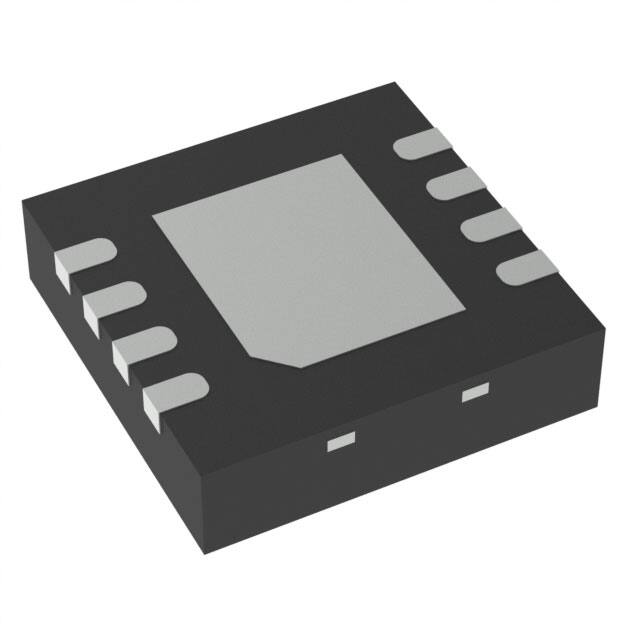
Small 2 mm × 2 mm 8-Pin SON Package
LDO Mode Voltage Regulation Options:
– 5.5V on bq24300
– 4.5V on bq24304
– 5.0V on bq24305
APPLICATIONS
•
•
Bluetooth Headsets
Low-Power Handheld Devices
DESCRIPTION
The bq24300 and bq24304 are highly integrated circuits designed to provide protection to Li-ion batteries from
failures of the charging circuit. The IC continuously monitors the input voltage, the input current, and the battery
voltage. The device operates like a linear regulator: for voltages up to the Input Overvoltage threshold, the output
is held at 5.5V (bq24300), 5.0V (bq24305) or 4.5V (bq24304). In case of an input overvoltage condition, if the
overvoltage condition persists for more than a few microseconds, the IC removes power from the charging circuit
by turning off an internal switch. In the case of an overcurrent condition, it limits the current to a safe value for a
blanking duration before turning the switch off. Additionally, the IC also monitors its own die temperature and
switches off if it becomes too hot.
The IC also offers optional protection against reverse voltage at the input with an external P-channel MOSFET.
PINOUT
APPLICATION SCHEMATIC
AC Adapter
IN
1
8
OUT
OUT 8
1 IN
VDC
GND
1 μF
1 μF
bq24080
Charger IC
PGATE
3
NC
4
7 NC
bq24300
bq24304
bq24305
bq2430x
SYSTEM
VBAT 6
6 VBAT
5
CE
100 kW
CE
2
VSS
VSS
2
5
1
2
Please be aware that an important notice concerning availability, standard warranty, and use in critical applications of Texas
Instruments semiconductor products and disclaimers thereto appears at the end of this data sheet.
PowerPAD is a trademark of Texas Instruments.
PRODUCTION DATA information is current as of publication date.
Products conform to specifications per the terms of the Texas
Instruments standard warranty. Production processing does not
necessarily include testing of all parameters.
Copyright © 2007–2009, Texas Instruments Incorporated
�bq24300
bq24304
bq24305
SLUS764C – AUGUST 2007 – REVISED DECEMBER 2009
www.ti.com
This integrated circuit can be damaged by ESD. Texas Instruments recommends that all integrated circuits be handled with
appropriate precautions. Failure to observe proper handling and installation procedures can cause damage.
ESD damage can range from subtle performance degradation to complete device failure. Precision integrated circuits may be more
susceptible to damage because very small parametric changes could cause the device not to meet its published specifications.
ORDERING INFORMATION (1)
DEVICE
(1)
(2)
(2)
OUTPUT REGULATION VOLTAGE
PACKAGE
MARKING
bq24300
5.5V
2mm x 2mm SON
BZA
bq24304
4.5V
2mm x 2mm SON
CBS
bq24305
5.0V
2mm x 2mm SON
DSG
For the most current package and ordering information, see the Package Option Addendum at the end of this document, or see the TI
website at www.ti.com.
To order a 3000 pcs reel add R to the part number, or to order a 250 pcs reel add T to the part number.
PACKAGE DISSIPATION RATINGS
(1)
PACKAGE
RθJC
DSG
5°C/W
RθJA
(1)
75°C/W
This data is based on using the JEDEC High-K board and the exposed die pad is connected to a Cu pad on the board. The pad is
connected to the ground plane by a 2x3 via matrix.
ABSOLUTE MAXIMUM RATINGS (1)
over operating free-air temperature range (unless otherwise noted)
PARAMETER
VALUE
UNIT
IN, PGATE (with respect to VSS)
–0.3 to 30
V
OUT (with respect to VSS)
–0.3 to 12
V
CE, VBAT (with respect to VSS)
–0.3 to 7
V
All (Human Body Model per JESD22-A114-E)
2000
V
All (Machine Model per JESD22-A115-A)
200
V
All (Charged Device Model per JESD22-C101-C)
500
V
15 (Air Discharge) 8
(Contact)
kV
Junction temperature, TJ
–40 to 150
°C
Storage temperature, TSTG
–65 to 150
°C
Input voltage
ESD Withstand voltage
PIN
IN (IEC 61000-4-2) (with IN pin bypassed to VSS with 1.0-μF low-ESR
ceramic capacitor)
(1)
Stresses beyond those listed under absolute maximum ratings may cause permanent damage to the device. These are stress ratings
only, and functional operation of the device at these or any other conditions beyond those indicated under recommended operating
conditions is not implied. Exposure to absolute-maximum-rated conditions for extended periods may affect device reliability.
RECOMMENDED OPERATING CONDITIONS
over operating free-air temperature range (unless otherwise noted)
MIN
VIN
Input voltage range
TJ
Junction temperature
2
Submit Documentation Feedback
MAX
UNIT
3.3
26
V
0
125
°C
Copyright © 2007–2009, Texas Instruments Incorporated
Product Folder Link(s): bq24300 bq24304 bq24305
�bq24300
bq24304
bq24305
www.ti.com
SLUS764C – AUGUST 2007 – REVISED DECEMBER 2009
ELECTRICAL CHARACTERISTICS
over junction temperature range 0°C ≤ TJ ≤ 125°C and recommended supply voltage (unless otherwise noted)
PARAMETER
TEST CONDITIONS
MIN
TYP
MAX
UNIT
POWER-ON-RESET
UVLO
Under-voltage lock-out, input
power detected threshold
CE = Low, VIN increasing from 0V to 3V
2.5
2.7
2.8
V
VHYS-UVLO
Hysteresis on UVLO
CE = Low, VIN decreasing from 3V to 0V
200
260
300
mV
tDGL(PGOOD)
Deglitch time, input power
detected status
CE = Low, time measured from
VIN 0V → 4V 1μs rise time, to output turning ON
8
ms
IN
bq24300
IDD
Operating
current
ISTDBY
Standby current
340
400
410
500
CE = High, VIN = 5V
65
95
μA
CE = Low, VIN = 4 V, IOUT = 250 mA
45
75
mV
5.30
5.5
5.70
4.36
4.5
4.64
4.85
5.0
5.15
10.2
10.5
10.8
V
60
100
160
mV
VIN = 5V, CE = Low, no load on OUT pin
bq24304,
bq24305
μA
INPUT TO OUTPUT CHARACTERISTICS
VDO
Drop-out voltage IN to OUT
OUTPUT VOLTAGE REGULATION
bq24300
VO(REG)
Output
voltage
bq24304
CE = Low, VIN = 6 V, IOUT = 250 mA
bq24305
V
INPUT OVERVOLTAGE PROTECTION
VOVP
Input overvoltage protection
threshold
CE = Low, VIN increasing from 4V to 12V
VHYS-OVP
Hysteresis on OVP
CE = Low, VIN decreasing from 12V to 4V
tBLANK(OVP)
Blanking time, on OVP
CE = Low, Time measured from
VIN 4V → 12V, 1μs rise time, to output turning OFF
tON(OVP)
Recovery time from input
overvoltage condition
CE = Low, Time measured from
VIN 12V → 4V, 1μs fall time, to output turning ON
64
μs
8
ms
INPUT OVERCURRENT PROTECTION
IOCP
Input overcurrent protection
range
CE = Low, VIN = 5 V
tBLANK(OCP)
Blanking time, input
overcurrent detected
CE = Low
5
ms
tREC(OCP)
Recovery time from input
overcurrent condition
CE = Low
64
ms
250
300
350
mA
BATTERY OVERVOLTAGE PROTECTION
BVOVP
Battery overvoltage
protection threshold
CE = Low, VIN > 4.4V, VVBAT increasing
from 4.2 V to 4.5 V
4.30
4.35
4.40
V
VHYS-BOVP
Hysteresis on BVOVP
CE = Low, VIN > 4.4V, VVBAT decreasing
from 4.5 V to 3.9 V
200
275
320
mV
IVBAT
Input bias current on the
VBAT pin
VVBAT = 4.4 V, TJ = 25°C
10
nA
tDGL(BOVP)
Deglitch time, battery
overvoltage detected
CE = Low, VIN > 4.4V, time measured from
VVBAT 4.2V → 4.5V, 1μs rise time to output turning OFF
μs
176
P-FET GATE DRIVER
VGCLMP
Gate driver clamp voltage
VIN > 17V
13
15
17
V
140
150
°C
THERMAL PROTECTION
TJ(OFF)
Thermal shutdown temperature
TJ(OFF-HYS)
Thermal shutdown hysteresis
20
°C
LOGIC LEVELS ON CE
VIL
Low-level input voltage
0
VIH
High-level input voltage
1.4
IIL
Low-level input current
Copyright © 2007–2009, Texas Instruments Incorporated
Product Folder Link(s): bq24300 bq24304 bq24305
0.4
V
1
μA
V
Submit Documentation Feedback
3
�bq24300
bq24304
bq24305
SLUS764C – AUGUST 2007 – REVISED DECEMBER 2009
www.ti.com
ELECTRICAL CHARACTERISTICS (continued)
over junction temperature range 0°C ≤ TJ ≤ 125°C and recommended supply voltage (unless otherwise noted)
PARAMETER
IIH
TEST CONDITIONS
High-level input current
MIN
VCE = 1.8V
TYP
MAX
15
UNIT
μA
Q1
IN
OUT
Charge Pump,
Bandgap,
Bias Gen
VREF
VISNS
VREF
VREF
Current Limiting Loop
VO(REG) Loop
OFF
OCP Comparator
VREF - D
tBLANK(OCP)
VISNS
VIN
CONTROL
VREF
AND STATUS
OVP Comparator
CE
tBLANK(OVP)
VIN
VREF
tDGL(PGOOD)
UVLO
VBAT
PGATE
level shift
VREF
THERMAL
SHUTDOWN
tDGL(BOVP)
V IN
V GCLMP
VSS
Figure 1. Simplified Block Diagram
4
Submit Documentation Feedback
Copyright © 2007–2009, Texas Instruments Incorporated
Product Folder Link(s): bq24300 bq24304 bq24305
�bq24300
bq24304
bq24305
www.ti.com
SLUS764C – AUGUST 2007 – REVISED DECEMBER 2009
TERMINAL FUNCTIONS
TERMINAL
NAME
NO.
I/O
DESCRIPTION
IN
1
I
Input power, connect to external DC supply. Connect external 0.1μF (minimum) ceramic capacitor to VSS
VSS
2
–
Ground terminal
PGATE
3
O
Gate drive for optional external P-FET
NC
4, 7
CE
5
I
Chip enable input. Active low. When CE = Hi, the input FET is off. Internally pulled down.
VBAT
6
I
Battery voltage sense input. Connect to pack positive terminal through a resistor.
8
O
Output terminal to the charging system. Connect external 1μF capacitor (minimum) ceramic capacitor to
VSS
OUT
Thermal PAD
Do not connect to any external circuit. These pins may have internal connections used for test purposes.
–
There is an internal electrical connection between the exposed thermal pad and the VSS pin of the device.
The thermal pad must be connected to the same potential as the VSS pin on the printed circuit board. Do
not use the thermal pad as the primary ground input for the device. VSS pin must be connected to ground at
all times.
IN
1
VSS
2
PGATE
3
NC
4
bq24300
bq24304
bq24305
8
OUT
7
NC
6
VBAT
5
CE
Copyright © 2007–2009, Texas Instruments Incorporated
Product Folder Link(s): bq24300 bq24304 bq24305
Submit Documentation Feedback
5
�bq24300
bq24304
bq24305
SLUS764C – AUGUST 2007 – REVISED DECEMBER 2009
www.ti.com
TYPICAL OPERATING PERFORMANCE
Test conditions (unless otherwise noted) for typical operating performance are: VIN = 5 V, CIN = 1 μF, COUT = 1μF,
RBAT = 100 kΩ, ROUT = 22Ω, TA = 25°C (see Figure 22 - Typical Application Circuit)
SPACER
SPACER
VIN
tDGL(PGOOD)
VOUT
VIN
VOUT
IOUT
IOUT
Figure 2. Normal Power-On Showing Soft-Start.
VIN 0 V to 6.0 V, tR = 20μs
Figure 3. Power-On with Input Overvoltage.
VIN 0 V to 12.0 V, tR = 50 μs
SPACER
SPACER
12.8V
11.5V
VIN
VIN
5.9V
5.92V
VOUT
VOUT
tBLANK(OVP)
Figure 4. bq24300 OVP Response for Input Step.
VIN 6.0 V to 10.3 V, tR = 2μs. Shows Immunity to Ringing
6
Submit Documentation Feedback
Figure 5. bq24300 OVP Response for Input Step.
VIN 6.0 V to 11.0 V, tR = 5μs. Shows OVP Blanking Time
Copyright © 2007–2009, Texas Instruments Incorporated
Product Folder Link(s): bq24300 bq24304 bq24305
�bq24300
bq24304
bq24305
www.ti.com
SLUS764C – AUGUST 2007 – REVISED DECEMBER 2009
TYPICAL OPERATING PERFORMANCE
SPACER
VIN < VUVLO VIN < VO(REG)
SPACER
VIN < VOVP
VIN
tON(OVP)
VIN
VOUT
VOUT
Figure 6. OUT Pin Response to Slow Input Ramp
Figure 7. bq24300 Recovery from Input OVP.
VIN 11.0 V to 5.0 V, tF = 400 μs
SPACER
SPACER
ROUT = 22W
VOUT
VIN
ROUT = 13W
VOUT
IOUT
IOUT
IOUT limited to 300mA
tREC(OCP)
tBLANK(OCP)
Figure 8. OCP, Powering up with OUT Pin Shorted to VSS
Figure 9. OCP, Showing Current Limiting and
OCP Blanking. ROUT 22Ω to 13Ω for 2.6 ms to 22Ω
Copyright © 2007–2009, Texas Instruments Incorporated
Product Folder Link(s): bq24300 bq24304 bq24305
Submit Documentation Feedback
7
�bq24300
bq24304
bq24305
SLUS764C – AUGUST 2007 – REVISED DECEMBER 2009
www.ti.com
TYPICAL OPERATING PERFORMANCE (continued)
SPACER
SPACER
ROUT = 22W
VOUT
ROUT = 13W
VOUT
IOUT
IOUT limited to 300mA
IOUT
tBLANK(OCP)
Figure 10. OCP, Showing Current Limiting and
OCP Blanking. ROUT 22Ω to 13Ω
Figure 11. Zoom-in on Turn-off Region of Figure 10, Showing
Soft-Stop
SPACER
VVBAT
tDGL(BOVP)
VOUT
Figure 12. Battery OVP. VVBAT Steps from 4.3 V to 4.5 V. Shows tDGL(BOVP) and Soft-Stop
8
Submit Documentation Feedback
Copyright © 2007–2009, Texas Instruments Incorporated
Product Folder Link(s): bq24300 bq24304 bq24305
�bq24300
bq24304
bq24305
www.ti.com
SLUS764C – AUGUST 2007 – REVISED DECEMBER 2009
TYPICAL OPERATING PERFORMANCE (continued)
UNDERVOLTAGE LOCKOUT
vs
FREE-AIR TEMPERATURE
DROPOUT VOLTAGE (IN to OUT)
vs
FREE-AIR TEMPERATURE
80
2.75
2.7
70
VDO @ 250mA - mV
VIN Increasing
VUVLO, VHYS-UVLO - V
2.65
2.6
2.55
60
bq24304, VIN = 4 V
50
bq24300, VIN = 5 V
40
2.5
VIN Decreasing
30
2.45
2.4
-50
20
-30
-10
10
30
50
70
Temperature - °C
90
110
0
130
50
100
150
Temperature - °C
Figure 13.
Figure 14.
REGULATION VOLTAGE (OUT pin)
vs
FREE-AIR TEMPERATURE
OVP THRESHOLD
vs
FREE-AIR TEMPERATURE
5.53
4.53
5.52
4.52
10.6
4.51
5.51
bq24300
VOVP, VHYS-OVP - V
bq24304
VO(REG) bq24304 - V
VO(REG) bq24300 - V
10.55
10.5
VIN Increasing
10.45
10.4
4.5
5.5
10.35
VIN Decreasing
4.4
5.49
0
20
40
60
80
Temperature - °C
100
120
10.3
0
20
40
60
80
100
120
Temperature - °C
Figure 15.
Figure 16.
Copyright © 2007–2009, Texas Instruments Incorporated
Product Folder Link(s): bq24300 bq24304 bq24305
Submit Documentation Feedback
9
�bq24300
bq24304
bq24305
SLUS764C – AUGUST 2007 – REVISED DECEMBER 2009
www.ti.com
TYPICAL OPERATING PERFORMANCE (continued)
OCP THRESHOLD
vs
FREE-AIR TEMPERATURE
BATTERY OVP THRESHOLDS
vs
FREE-AIR TEMPERATURE
4.4
315
4.35
310
BVOVP (VVBAT Increasing)
4.3
BVOVP - V
IOCP - mA
305
300
295
4.2
4.15
290
285
0
4.25
4.1
20
40
60
80
Temperature - °C
100
4.05
-50
120
Bat-OVP Recovery (VVBAT Decreasing)
-30
-10
10
30
50
70
Temperature - °C
Figure 17.
Figure 18.
LEAKAGE CURRENT (BAT pin)
vs
FREE-AIR TEMPERATURE
SUPPLY CURRENT
vs
INPUT VOLTAGE
90
110
130
900
2.5
800
2
700
IDD, ISTDBY - mA
CE = L
IVBAT - nA
1.5
1
600
500
400
300
CE = H
200
0.5
100
0
0
20
40
60
80
Temperature - °C
100
120
0
0
5
10
Submit Documentation Feedback
20
25
30
35
VIN - V
Figure 19.
10
15
Figure 20.
Copyright © 2007–2009, Texas Instruments Incorporated
Product Folder Link(s): bq24300 bq24304 bq24305
�bq24300
bq24304
bq24305
www.ti.com
SLUS764C – AUGUST 2007 – REVISED DECEMBER 2009
TYPICAL OPERATING PERFORMANCE (continued)
PGATE VOLTAGE
vs
INPUT VOLTAGE
18
16
14
VPGATE - V
12
10
8
6
4
2
0
0
5
10
15
20
25
30
35
VIN - V
Figure 21.
Copyright © 2007–2009, Texas Instruments Incorporated
Product Folder Link(s): bq24300 bq24304 bq24305
Submit Documentation Feedback
11
�bq24300
bq24304
bq24305
SLUS764C – AUGUST 2007 – REVISED DECEMBER 2009
www.ti.com
TYPICAL APPLICATION CIRCUITS
AC Adapter
1 IN
VDC
CIN
GND
OUT 8
COUT
1 μF
1 μF
bq24080
Charger IC
bq2430x
RBAT
SYSTEM
VBAT 6
VSS
CE
100 KΩ
2
5
Figure 22. Overvoltage, Overcurrent, and Battery Overvoltage Protection
AC Adapter
QEXT
VDC
GND
1 μF
100 kW
1
IN
OUT 8
3 PGATE
1 μF
bq2430x
bq24080
Charger IC
100 kW
SYSTEM
VBAT 6
RBAT
VSS
47 kW
CE 5
RCE
2
Figure 23. OVP, OCP, BATOVP With Input Reverse-Polarity Protection
12
Submit Documentation Feedback
Copyright © 2007–2009, Texas Instruments Incorporated
Product Folder Link(s): bq24300 bq24304 bq24305
�bq24300
bq24304
bq24305
www.ti.com
SLUS764C – AUGUST 2007 – REVISED DECEMBER 2009
DETAILED FUNCTIONAL DESCRIPTION
The bq24300 and bq24304 are highly integrated circuits designed to provide protection to Li-ion batteries from
failures of the charging circuit. The IC continuously monitors the input voltage, the input current and the battery
voltage, and protects down-stream circuitry from damage if any of these parameters exceeds safe values. The IC
also monitors its own die temperature and switches off if it becomes too hot.
The IC also offers optional protection against reverse voltage at the input with an external P-channel MOSFET.
POWER DOWN
The device remains in power down mode when the input voltage at the IN pin is below the under-voltage
threshold VUVLO. The FET Q1 (see Figure 1) connected between IN and OUT pins is off.
POWER-ON RESET
The device resets all internal timers when the input voltage at the IN pin exceeds the UVLO threshold. The gate
driver for the external P-FET is enabled. The IC then waits for duration tDGL(PGOOD) for the input voltage to
stabilize. If, after tDGL(PGOOD), the input voltage and battery voltage are safe, FET Q1 is turned ON. The IC has a
soft-start feature to control the inrush current. This soft-start minimizes voltage ringing at the input (the ringing
occurs because the parasitic inductance of the adapter cable and the input bypass capacitor form a resonant
circuit). Figure 2 shows the power-up behavior of the device. Because of the deglitch time at power-on, if the
input voltage rises rapidly to beyond the OVP threshold, the device will not switch on at all, as shown in Figure 3.
OPERATION
The device continuously monitors the input voltage, the input current and the battery voltage as described in
detail in the following sections:
Input Overvoltage Protection
As long as the input voltage is less than VO(REG), the output voltage tracks the input voltage (less the drop caused
by RDSON of Q1). If the input voltage is greater than VO(REG) (plus the RDSON drop) and less than VOVP, the
device acts like a series linear regulator, with the output voltage regulated to VO(REG). If the input voltage rises
above VOVP, the output voltage is clamped to VO(REG) for a blanking duration tBLANK(OVP). If the input voltage
returns below VOVP within tBLANK(OVP), the device continues normal operation (see Figure 4). This provides
protection against turning power off due to transient overvoltage spikes while still protecting the system.
However, if the input voltage remains above VOVP for more than tBLANK(OVP), the internal FET is turned off,
removing power from the circuit (see Figure 5). When the input voltage comes back to a safe value, the device
waits for tON(OVP) then switches on Q1 and goes through the soft-start routine (see Figure 7).
Figure 6 describes graphically the behavior of the OUT pin over the entire range of input voltage variation.
Input Overcurrent Protection
The device can supply load current up to IOCP continuously. If the load current tries to exceed this threshold, the
current is limited to IOCP for a maximum duration of tBLANK(OCP). If the load current returns to less than IOCP before
tBLANK(OCP) times out, the device continues to operate (see Figure 9). However, if the overcurrent situation
persists for tBLANK(OCP), FET Q1 is turned off for a duration of tREC(OCP). It is then turned on again and the current
is monitored all over again (see Figure 10 and Figure 8).
To prevent the input voltage from spiking up due to the inductance of the input cable, Q1 is not turned off rapidly
in an overcurrent fault condition. Instead, the gate drive of Q1 is reduced slowly, resulting in a “soft-stop”, as
shown in Figure 11.
Battery Overvoltage Protection
The battery overvoltage threshold BVOVP is internally set to 4.35V. If the battery voltage exceeds the BVOVP
threshold for longer than tDGL(BOVP), FET Q1 is turned off (see Figure 12). This switch-off is also a soft-stop. Q1 is
turned ON (soft-start) once the battery voltage drops to BVOVP – VHYS-BOVP.
Copyright © 2007–2009, Texas Instruments Incorporated
Product Folder Link(s): bq24300 bq24304 bq24305
Submit Documentation Feedback
13
�bq24300
bq24304
bq24305
SLUS764C – AUGUST 2007 – REVISED DECEMBER 2009
www.ti.com
Thermal Protection
If the junction temperature of the device exceeds TJ(OFF), FET Q1 is turned off. The FET is turned back on when
the junction temperature falls below TJ(OFF) – TJ(OFF-HYS).
Enable Function
The IC has an enable pin which can be used to enable or disable the device. When the CE pin is driven high, the
internal FET is turned off. When the CE pin is low, the FET is turned on if other conditions are safe. The CE pin
has an internal pull-down resistor of 200 kΩ (typical) and can be left floating.
PGATE Pin
When used with an external P-Channel MOSFET, in addition to OVP, OCP and Battery-OVP, the device offers
protection against input reverse polarity up to –30V. When operating with normal polarity, the IC first turns on
due to current flow through the body-diode of the FET QEXT. The PGATE pin then goes low, turning ON QEXT.
For input voltages larger than VGCLMP, the voltage on the PGATE pin is driven to VIN – VGCLMP. This ensures that
the gate to source voltage seen by QEXT does not exceed –VGCLMP.
14
Submit Documentation Feedback
Copyright © 2007–2009, Texas Instruments Incorporated
Product Folder Link(s): bq24300 bq24304 bq24305
�bq24300
bq24304
bq24305
www.ti.com
SLUS764C – AUGUST 2007 – REVISED DECEMBER 2009
Any State
If VIN < VUVLO,
go to Power Down
Power Down
All IC functions OFF
No
VIN > VUVLO?
Yes
Reset
Timers reset
Q1 off
Turn on PGATE
No
CE = Low ?
Yes
VIN < VOVP ?
Turn off Q1
No
Yes
I < IOCP ?
Turn off Q1
No
Wait tREC(OCP)
Yes
VVBAT < BVOVP ?
TJ < TJ(OFF) ?
Turn off Q1
No
No
Turn off Q1
Yes
Turn on Q1
Figure 24. Flow Diagram
Copyright © 2007–2009, Texas Instruments Incorporated
Product Folder Link(s): bq24300 bq24304 bq24305
Submit Documentation Feedback
15
�bq24300
bq24304
bq24305
SLUS764C – AUGUST 2007 – REVISED DECEMBER 2009
www.ti.com
APPLICATION INFORMATION
Selection of RBAT:
It is strongly recommended that the battery not be tied directly to the VBAT pin of the device, as under some
failure modes of the IC, the voltage at the IN pin may appear on the VBAT pin. This voltage can be as high as
30V, and applying 30V to the battery in case of the failure of the device can be hazardous. Connecting the VBAT
pin through RBAT prevents a large current from flowing into the battery in case of failure of the IC. In the interests
of safety, RBAT should have a very high value. The problem with a large RBAT is that the voltage drop across this
resistor because of the VBAT bias current IVBAT causes an error in the BVOVP threshold. This error is over and
above the tolerance on the nominal 4.35V BVOVP threshold.
Choosing RBAT in the range 100KΩ to 470kΩ is a good compromise. In the case of IC failure, with RBAT equal to
100kΩ, the maximum current flowing into the battery would be (30V – 3V) ÷ 100kΩ = 270μA, which is low
enough to be absorbed by the bias currents of the system components. RBAT equal to 100kΩ would result in a
worst-case voltage drop of RBAT X IVBAT ≈ 1mV. This is negligible compared to the internal tolerance of 50mV on
the BVOVP threshold.
If the Bat-OVP function is not required, the VBAT pin should be connected to VSS.
Selection of RCE:
The CE pin can be used to enable and disable the IC. If host control is not required, the CE pin can be tied to
ground or left un-connected, permanently enabling the device.
In applications where external control is required, the CE pin can be controlled by a host processor. As in the
case of the VBAT pin (see above), the CE pin should be connected to the host GPIO pin through as large a
resistor as possible. The limitation on the resistor value is that the minimum VOH of the host GPIO pin less the
drop across the resistor should be greater than VIH of the bq2430x CE pin. The drop across the resistor is given
by RCE X IIH.
Selection of Input and Output Bypass Capacitors:
The input capacitor CIN in Figure 22 and Figure 23 is for decoupling, and serves an important purpose.
Whenever there is a step change downwards in the system load current, the inductance of the input cable
causes the input voltage to spike up. CIN prevents the input voltage from overshooting to dangerous levels. It is
strongly recommended that a ceramic capacitor of at least 1μF be used at the input of the device. It should be
located in close proximity to the IN pin.
COUT in Figure 23 is also important: If a fast (< 1μs rise-time) overvoltage transient occurs at the input, the
current that charges COUT causes the device’s current-limiting loop to kick in, reducing the gate-drive to FET Q1.
This results in improved performance for input overvoltage protection. COUT should also be a ceramic capacitor of
at least 1μF, located close to the OUT pin. COUT also serves as the input decoupling capacitor for the charging
circuit downstream of the protection IC.
PCB Layout Guidelines:
1. This device is a protection device, and is meant to protect down-stream circuitry from hazardous voltages.
Potentially, high voltages may be applied to this IC. It has to be ensured that the edge-to-edge clearances of
PCB traces satisfy the design rules for the maximum voltages expected to be seen in the system.
2. The device uses SON packages with a PowerPAD™. For good thermal performance, the PowerPAD should
be thermally coupled with the PCB ground plane. In most applications, this will require a copper pad directly
under the IC. This copper pad should be connected to the ground plane with an array of thermal vias.
3. CIN and COUT should be located close to the IC. Other components like RBAT should also be located close to
the IC.
16
Submit Documentation Feedback
Copyright © 2007–2009, Texas Instruments Incorporated
Product Folder Link(s): bq24300 bq24304 bq24305
�bq24300
bq24304
bq24305
www.ti.com
SLUS764C – AUGUST 2007 – REVISED DECEMBER 2009
REVISION HISTORY
Changes from Original (August 2007) to Revision A
•
Page
Changed the devices from Product Preview status to Production. ...................................................................................... 1
Changes from Revision A (October 2007) to Revision B
Page
•
Added device bq24305 to the data sheet ............................................................................................................................. 1
•
Changed the bq24305 marking in the Ordering Information table From CHD To: DSG ...................................................... 2
•
Changed Figure 22, Overvoltage, Overcurrent, and Battery Overvoltage Protection ........................................................ 12
•
Changed Figure 23, OVP, OCP, BATOVP With Input Reverse-Polarity Protection ........................................................... 12
Changes from Revision B (September 2009) to Revision C
Page
•
Deleted Lead temperature (soldering, 10 seconds) from the Abs Max table. This is covered in the Package
information. ........................................................................................................................................................................... 2
•
Changed Recommended Operating Conditions, Input voltage range - MAX value From 30V To: 26V .............................. 2
•
Changed BVOVP test conditions - From: CE = Low, VIN > 4.3V, VVBAT increasing To: CE = Low, VIN > 4.4V, VVBAT
increasing .............................................................................................................................................................................. 3
•
Changed VHYS-BOVP test conditions - From: CE = Low, VIN > 4.3V, VVBAT decreasing To: CE = Low, VIN > 4.4V, VVBAT
decreasing ............................................................................................................................................................................ 3
•
Changed the Gate driver clamp voltage Typ valur From: 14V To: 15V and the Max value From: 15V To: 17V ................. 3
•
Changed Figure 23, OVP, OCP, BATOVP With Input Reverse-Polarity Protection ........................................................... 12
•
Changed section - Selection of RBAT text From: (30V – 3V) x 100kΩ = 246μA To: battery would be (30V – 3V) ÷
100kΩ = 270μA ................................................................................................................................................................... 16
Copyright © 2007–2009, Texas Instruments Incorporated
Product Folder Link(s): bq24300 bq24304 bq24305
Submit Documentation Feedback
17
�PACKAGE OPTION ADDENDUM
www.ti.com
29-Apr-2022
PACKAGING INFORMATION
Orderable Device
Status
(1)
Package Type Package Pins Package
Drawing
Qty
Eco Plan
(2)
Lead finish/
Ball material
MSL Peak Temp
Op Temp (°C)
Device Marking
(3)
(4/5)
(6)
BQ24300DSGR
ACTIVE
WSON
DSG
8
3000
RoHS & Green NIPDAU | NIPDAUAG
Level-2-260C-1 YEAR
0 to 125
BZA
BQ24300DSGT
ACTIVE
WSON
DSG
8
250
RoHS & Green NIPDAU | NIPDAUAG
Level-2-260C-1 YEAR
0 to 125
BZA
BQ24305DSGR
ACTIVE
WSON
DSG
8
3000
RoHS & Green
NIPDAUAG
Level-2-260C-1 YEAR
0 to 125
DSG
BQ24305DSGT
ACTIVE
WSON
DSG
8
250
RoHS & Green
NIPDAUAG
Level-2-260C-1 YEAR
0 to 125
DSG
(1)
The marketing status values are defined as follows:
ACTIVE: Product device recommended for new designs.
LIFEBUY: TI has announced that the device will be discontinued, and a lifetime-buy period is in effect.
NRND: Not recommended for new designs. Device is in production to support existing customers, but TI does not recommend using this part in a new design.
PREVIEW: Device has been announced but is not in production. Samples may or may not be available.
OBSOLETE: TI has discontinued the production of the device.
(2)
RoHS: TI defines "RoHS" to mean semiconductor products that are compliant with the current EU RoHS requirements for all 10 RoHS substances, including the requirement that RoHS substance
do not exceed 0.1% by weight in homogeneous materials. Where designed to be soldered at high temperatures, "RoHS" products are suitable for use in specified lead-free processes. TI may
reference these types of products as "Pb-Free".
RoHS Exempt: TI defines "RoHS Exempt" to mean products that contain lead but are compliant with EU RoHS pursuant to a specific EU RoHS exemption.
Green: TI defines "Green" to mean the content of Chlorine (Cl) and Bromine (Br) based flame retardants meet JS709B low halogen requirements of


 工商网监
湘ICP备2023018690号
工商网监
湘ICP备2023018690号
