Product
Folder
Sample &
Buy
Support &
Community
Tools &
Software
Technical
Documents
bq24380, bq24381, bq24382
SLUS805C – APRIL 2008 – REVISED AUGUST 2015
bq2438x Overvoltage and Overcurrent Protection IC and Li+ Charger
Front-End Protection IC With LDO Mode
1 Features
3 Description
•
•
•
•
•
•
•
•
•
•
•
The bq2438x family of devices are charger front-end
integrated circuits (ICs) designed to provide
protection to Li-ion batteries from failures of the
charging circuit. The device continuously monitors the
input voltage and battery voltage. The device
operates like a linear regulator, maintaining a 5.5-V
(bq24380) or 5-V (bq24381, bq24382) output with
input voltages up to the Input overvoltage threshold.
During input overvoltage conditions, the device
immediately turns off the internal pass FET
disconnecting the charging circuit from the damaging
input source. Additionally, if the battery voltage rises
to unsafe levels while charging, power is removed
from the system. The device checks for short-circuit
or overload conditions at its output when turning the
pass FET on, and if it finds unsafe conditions, it
switches off and then rechecks the conditions.
Additionally, the device also monitors its die
temperature and switches off if it exceeds 140°C.
1
Input Overvoltage Protection
Accurate Battery Overvoltage Protection
Output Short-Circuit Protection
Soft-Start to Prevent Inrush Currents
Soft-Stop to Prevent Voltage Spikes
Maximum Input Voltage of 30 V
Supports up to 1.7-A Load Current
Thermal Shutdown
Enable Function
Fault Status Indication
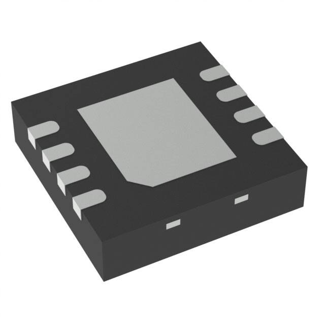
Small 2 mm × 2 mm 8-Pin WSON Package
2 Applications
•
•
•
•
Smart Phones, Mobile Phones
PDAs
MP3 Players
Low-Power Handheld Devices
When the device is controlled by a processor, the
device provides status information about fault
conditions to the host.
Device Information(1)
PART NUMBER
PACKAGE
BODY SIZE (NOM)
bq24380
bq24381
WSON (8)
2.00 mm × 2.00 mm
bq24382
(1) For all available packages, see the orderable addendum at
the end of the data sheet.
Simplified Schematic
AC Adapter
OUT 8
1 IN
VDC
GND
Charging
Circuit
1 mF
1 mF
bq24380
SYSTEM
VBAT 6
VSS
2
1
An IMPORTANT NOTICE at the end of this data sheet addresses availability, warranty, changes, use in safety-critical applications,
intellectual property matters and other important disclaimers. PRODUCTION DATA.
�bq24380, bq24381, bq24382
SLUS805C – APRIL 2008 – REVISED AUGUST 2015
www.ti.com
Table of Contents
1
2
3
4
5
6
7
Features ..................................................................
Applications ...........................................................
Description .............................................................
Revision History.....................................................
Pin Configuration and Functions .........................
Specifications.........................................................
1
1
1
2
3
4
6.1
6.2
6.3
6.4
6.5
6.6
6.7
4
4
4
4
5
6
7
Absolute Maximum Ratings ......................................
ESD Ratings ............................................................
Recommended Operating Conditions.......................
Thermal Information ..................................................
Electrical Characteristics...........................................
Timing Requirements ................................................
Typical Characteristics ..............................................
Detailed Description .............................................. 9
7.1 Overview ................................................................... 9
7.2 Functional Block Diagram ......................................... 9
7.3 Feature Description................................................. 10
7.4 Device Functional Modes........................................ 11
8
Application and Implementation ........................ 12
8.1 Application Information............................................ 12
8.2 Typical Application ................................................. 12
9 Power Supply Recommendations...................... 15
10 Layout................................................................... 15
10.1 Layout Guidelines ................................................. 15
10.2 Layout Example .................................................... 15
11 Device and Documentation Support ................. 16
11.1
11.2
11.3
11.4
11.5
Related Links ........................................................
Community Resources..........................................
Trademarks ...........................................................
Electrostatic Discharge Caution ............................
Glossary ................................................................
16
16
16
16
16
12 Mechanical, Packaging, and Orderable
Information ........................................................... 16
4 Revision History
NOTE: Page numbers for previous revisions may differ from page numbers in the current version.
Changes from Revision B (March 2009) to Revision C
Page
•
Added ESD Ratings table, Thermal Information, Timing Requirements, Functional Block Diagram, Design
Requirements, Application Curves, Power Supply Recommendations, Layout Example, Device and Documentation
Support, and Mechanical, Packaging, and Orderable Information......................................................................................... 1
•
Changed SON to WSON throughout the document............................................................................................................... 1
•
Changed From: "the bq2430x CE pin." To: "the bq2438x CE pin." in Selection of R(BAT) ................................................... 13
•
Moved Figures 1 through 8 from Typical Characteristics to Application Curves section ..................................................... 13
Changes from Revision A (May 2008) to Revision B
Page
•
Added device bq24382 to the datasheet................................................................................................................................ 1
•
Added the bq24382 option to IDD in the Electrical Characteristics. ........................................................................................ 5
•
Added the bq24382 option to VO(REG) in the Electrical Characteristics................................................................................... 5
•
Added the bq24382 option to VOVP in the Electrical Characteristics ...................................................................................... 5
•
Added the bq24382 option to Vhys(OVP) in the Electrical Characteristics ................................................................................. 5
Changes from Original (April 2008) to Revision A
Page
•
Changed Figure 4 .................................................................................................................................................................. 7
•
Changed Figure 5 .................................................................................................................................................................. 7
•
Added Figure 9 ...................................................................................................................................................................... 7
2
Submit Documentation Feedback
Copyright © 2008–2015, Texas Instruments Incorporated
Product Folder Links: bq24380 bq24381 bq24382
�bq24380, bq24381, bq24382
www.ti.com
SLUS805C – APRIL 2008 – REVISED AUGUST 2015
5 Pin Configuration and Functions
DSG Package
8-Pin WSON With Exposed Thermal Pad
Top View
IN
1
8
OUT
VSS
2
7
NC
NC
3
6
VBAT
FAULT
4
5
CE
Pin Functions
PIN
NAME
NO.
I/O
DESCRIPTION
CE
5
I
Active-low chip enable input. Connect CE = HI to turn the input pass FET off. Connect CE = LOW to turn the
internal pass FET on and connect the input to the charging circuitry. CE is Internally pulled down,
approximately 200 kΩ.
FAULT
4
O
Open-drain device status output. FAULT is pulled to VSS internally when the input pass FET has been turned
off due to input overvoltage or output short-circuit conditions, an overtemperature condition, or because the
battery voltage is outside safe limits. FAULT is high impedance during normal operation.
IN
1
I
Input power, connected to external DC supply. Bypass IN to VSS with a ceramic capacitor (1 μF minimum)
NC
3, 7
Output terminal to the charging system. Bypass OUT to VSS with a ceramic capacitor (1 μF minimum)
6
I
Battery voltage sense input. Connected to pack positive terminal through a 100-kΩ resistor.
2
–
Ground terminal. Connect to the thermal pad and to the ground rail of the circuit.
8
VBAT
VSS
Thermal PAD
Do not connect to any external circuits. These pins may have internal connections used for test purposes.
O
OUT
There is an internal electrical connection between the exposed thermal pad and the VSS pin of the device. The
thermal pad must be connected to the same potential as the VSS pin on the printed-circuit board. Do not use
the thermal pad as the primary ground input for the device. VSS pin must be connected to ground at all times.
Copyright © 2008–2015, Texas Instruments Incorporated
Product Folder Links: bq24380 bq24381 bq24382
Submit Documentation Feedback
3
�bq24380, bq24381, bq24382
SLUS805C – APRIL 2008 – REVISED AUGUST 2015
www.ti.com
6 Specifications
6.1 Absolute Maximum Ratings
over operating free-air temperature range (unless otherwise noted) All voltage values are with respect to the network ground
terminal unless otherwise noted. (1)
VI
Input voltage
IOUTmax
MIN
MAX
IN (with respect to VSS)
–0.3
30
OUT (with respect to VSS)
–0.3
12
FAULT, CE, VBAT (with respect to VSS)
–0.3
7
UNIT
V
Output source current
OUT
2
A
Output sink current
FAULT
15
mA
TJ
Junction temperature
–40
150
°C
Tstg
Storage temperature
–65
150
°C
(1)
Stresses beyond those listed under Absolute Maximum Ratings may cause permanent damage to the device. These are stress ratings
only, which do not imply functional operation of the device at these or any other conditions beyond those indicated under Recommended
Operating Conditions. Exposure to absolute-maximum-rated conditions for extended periods may affect device reliability.
6.2 ESD Ratings
VALUE
V(ESD)
(1)
(2)
Electrostatic discharge
Human-body model (HBM), per ANSI/ESDA/JEDEC JS-001 (1)
±2000
Charged-device model (CDM), per JEDEC specification JESD22C101 (2)
±500
UNIT
V
JEDEC document JEP155 states that 500-V HBM allows safe manufacturing with a standard ESD control process.
JEDEC document JEP157 states that 250-V CDM allows safe manufacturing with a standard ESD control process.
6.3 Recommended Operating Conditions
MIN
VI
IN voltage range
IO
Output current, OUT pin
TJ
Junction temperature
NOM
MAX
UNIT
3.3
30
V
1.7
A
–40
125
°C
6.4 Thermal Information
bq2438x
THERMAL METRIC (1)
DSG (WSON)
UNIT
8 PINS
RθJA
Junction-to-ambient thermal resistance
64
°C/W
RθJC(top)
Junction-to-case (top) thermal resistance
84.1
°C/W
RθJB
Junction-to-board thermal resistance
33.9
°C/W
ψJT
Junction-to-top characterization parameter
1.9
°C/W
ψJB
Junction-to-board characterization parameter
34.3
°C/W
RθJC(bot)
Junction-to-case (bottom) thermal resistance
5.8
°C/W
(1)
4
For more information about traditional and new thermal metrics, see the Semiconductor and IC Package Thermal Metrics application
report, SPRA953.
Submit Documentation Feedback
Copyright © 2008–2015, Texas Instruments Incorporated
Product Folder Links: bq24380 bq24381 bq24382
�bq24380, bq24381, bq24382
www.ti.com
SLUS805C – APRIL 2008 – REVISED AUGUST 2015
6.5 Electrical Characteristics
Over junction temperature range –40°C ≤ TJ ≤ 125°C and recommended supply voltage (unless otherwise noted)
PARAMETER
TEST CONDITIONS
MIN
TYP
MAX
UNIT
IN
UVLO
Undervoltage lock-out, input power
detected threshold
CE = LO or HI, VIN: 0 V → 3 V
Vhys(UVLO)
Hysteresis on UVLO
CE = LO or HI, VIN: 3 V → 0 V
IDD
ISTDBY
CE = LO, no load on OUT pin,
VIN = 5 V
Operating current
Standby current
2.5
2.8
V
200
300
mV
bq24380
250
bq24381
300
bq24382
300
μA
CE = HI, VIN = 5.5 V
100
μA
280
mV
10
μA
INPUT-TO-OUTPUT CHARACTERISTICS
VDO
Dropout voltage IN to OUT
CE = LO, VIN = 5 V, I(OUT) = 1 A
IOFF
Q1 off-state leakage current
CE = HI, VIN = 5.5 V
INPUT OVERVOLTAGE PROTECTION
VO(REG)
VOVP
Output voltage
CE = LO, VIN = 6 V
Input overvoltage protection threshold
CE = LO, VIN: 5 V → 8 V
CE = LO or HI, VIN: 7 V → 5 V
Vhys(OVP)
Hysteresis on OVP
CE = LO or HI, VIN: 8 V → 5 V
bq24380
5.3
5.5
5.7
bq24381
4.8
5
5.2
bq24382
4.8
5
5.2
bq24380
6.1
6.3
6.5
bq24831
6.88
7.1
7.31
bq24382
10.17
10.5
10.83
bq24380
25
110
bq24831
25
120
bq24382
150
300
V
V
mV
OUTPUT SHORT-CIRCUIT PROTECTION (ONLY at START-UP)
IO(SC)
Short-circuit detection threshold
tREC(SC)
Retry interval if short-circuit detected
3 V < VIN < VOVP - Vhys(OVP)
1.3
1.5
1.7
64
A
ms
BATTERY OVERVOLTAGE PROTECTION
BVOVP
Battery overvoltage protection threshold
VIN > 4.5 V, CE = LO
4.3
Vhys(BVovp)
Hysteresis on BV(OVP)
VIN > 4.5 V, CE = LO
200
I(VBAT)
Input bias current on VBAT pin
TJ = 25°C
4.35
4.4
V
320
mV
10
nA
150
°C
THERMAL PROTECTION
TJ(OFF)
Thermal shutdown temperature
TJ(OFF-HYS)
Thermal shutdown hysteresis
140
20
°C
LOGIC LEVELS ON CE
VIL
Logic LOW input voltage
0
VIH
Logic HIGH input voltage
1.4
0.4
V
1
μA
V CE = 1.8 V
15
μA
IIL
IIH
V
LOGIC LEVELS ON FAULT
VOL
Output LOW voltage
ISINK = 5 mA
0.2
V
Ilkg
Off-state leakage current, HI-Z
V FAULT = 5 V
10
μA
Copyright © 2008–2015, Texas Instruments Incorporated
Product Folder Links: bq24380 bq24381 bq24382
Submit Documentation Feedback
5
�bq24380, bq24381, bq24382
SLUS805C – APRIL 2008 – REVISED AUGUST 2015
www.ti.com
6.6 Timing Requirements
MIN
NOM
MAX
UNIT
IN
CE = LO or HI. Time measured from
VIN 0 V → 5 V 1-μs rise-time
Deglitch time, input power detected
status
tDGL(PGOOD)
8
ms
200
ns
8
ms
176
μs
INPUT OVERVOLTAGE PROTECTION
tPD(OVP)
(1)
tREC(OVP)
Input OV propagation delay
VIN: 5 V → 10 V
Recovery time from input overvoltage
condition
CE = LO. Time measured from
V IN: 7 V → 5 V, 1-μs fall-time
BATTERY OVERVOLTAGE PROTECTION
(1)
VIN > 4.5 V, CE = LO, Time measured
from VVSAT rising from 4.1 V to 4.4 V
to FAULT going low.
Deglitch time, battery overvoltage
detected
tDGL(BVovp)
Not tested. Specified by design
tSStart
tCHK(SC)
t
tSStopREC(SC)
tSStart
tPD(OVP)
tDGL(BVOVP)
tDGL(PGOOD)
tREC(OVP)
5
VOVP
VOVP-Vhys(OVP)
VO(REG)
Input
Voltage
UVLO
2
4
2
2
4
6
VO(REG)
1
Output
Voltage
7
IO(SC)
Output
Current
CE
FAULT
3
BV(OVP)
BV(OVP)-Vhys(BVOVP)
Battery
Voltage
1.
Short-circuit during start-up
2.
Normal start-up condition
3.
Battery overvoltage event
4.
VUVLO < VIN < V(OREG) – VOUT tracks VIN
5.
Input overvoltage event
6.
Input below UVLO
7.
High-current event during normal operation
Figure 1. Timing Diagram
6
Submit Documentation Feedback
Copyright © 2008–2015, Texas Instruments Incorporated
Product Folder Links: bq24380 bq24381 bq24382
�bq24380, bq24381, bq24382
www.ti.com
SLUS805C – APRIL 2008 – REVISED AUGUST 2015
6.7 Typical Characteristics
250
2.75
IOUT = 1 A
210
VIN Rising
DROPOUT VOLTAGE - mV
UVLO - Undervoltage Lockout - V
2.70
2.65
2.60
2.55
2.50
VIN Falling
VIN = 4 V
170
VIN = 5 V
130
90
2.45
2.40
-40
-15
10
35
60
85
TA - Free-Air Temperature - °C
110
50
-40
135
-15
10
35
60
85
110
135
TA - Free-Air Temperature - °C
Figure 2. UVLO vs Free-Air Temperature
Figure 3. Dropout Voltage vs Free-Air Temperature
5.60
7.4
bq24381
VIN Rising
7.2
bq24380
5.40
VOVP – Threshold – V
VOUT(REG) – Output Voltage – V
5.50
5.30
5.20
5.10
7.0
VIN Falling
6.8
6.6
VIN Rising
6.4
bq24381
6.2
5.00
4.90
–40
–15
10
35
60
85
110
bq24380
6.0
–40
135
–15
TA – Free-Air Temperature – °C
VIN Falling
10
35
60
85
TA – Free-Air Temperature – °C
110
135
Figure 5. OVP Threshold vs Free-Air Temperature
Figure 4. Output Voltage Regulation, VO(REG) vs Free-Air
Temperature
4.40
25
4.35
IIkg - Bat Leakage Current - nA
VBOVP - Threshold - V
VBAT Rising
4.30
4.25
4.20
4.15
15
10
5
VBAT Falling
4.10
4.05
-40
20
-15
10
35
60
85
TA - Free-Air Temperature - °C
110
135
Figure 6. OVP Threshold, VBOVP vs Free-Air Temperature
0
-40
-15
10
35
60
85
TA - Free-Air Temperature - °C
110
135
Figure 7. Leakage Current (VBAT PIN) vs Free-Air
Temperature
Copyright © 2008–2015, Texas Instruments Incorporated
Product Folder Links: bq24380 bq24381 bq24382
Submit Documentation Feedback
7
�bq24380, bq24381, bq24382
SLUS805C – APRIL 2008 – REVISED AUGUST 2015
www.ti.com
Typical Characteristics (continued)
1000
1000
900
900
VO(REG)
700
IC Enabled
600
500
400
300
IC Disabled
200
IC Enabled
600
500
400
300
IC Disabled
100
0
5
10
15
20
VIN – Input Voltage – V
25
30
Figure 8. Supply Current vs Input Voltage (bq24380)
8
700
200
100
0
VO(REG)
800
ICC – Supply Current – mA
ICC – Supply Current – mA
800
Submit Documentation Feedback
0
0
5
10
15
20
VIN – Input Voltage – V
25
30
Figure 9. Supply Current vs Input Voltage (bq24381)
Copyright © 2008–2015, Texas Instruments Incorporated
Product Folder Links: bq24380 bq24381 bq24382
�bq24380, bq24381, bq24382
www.ti.com
SLUS805C – APRIL 2008 – REVISED AUGUST 2015
7 Detailed Description
7.1 Overview
The bq2438x is a highly integrated circuit designed to provide protection to Li-ion batteries from failures of the
charging circuit and the input source. The device continuously monitors the input voltage and the battery voltage.
The device operates like a linear regulator, maintaining a 5.5-V (bq24380) or 5-V (bq24381, bq24382) output with
input voltages up to the input overvoltage threshold (VOVP). If the input voltage exceeds VOVP, the device shuts
off the pass FET and disconnects the system from input power. Additionally, if the battery voltage rises above
4.35 V, the device switches off the pass FET, removing the power from the system until the battery voltage falls
to safe levels. The device also monitors its die temperature and switches the pass FET off if it exceeds 140°C.
The device can be controlled by a processor, and also provides status information about fault conditions to the
host.
7.2 Functional Block Diagram
Q1
IN
OUT
Output Regulation
Loop
VO(REG)
1.5A
Short Circuit protection
Disabled after startup
Chargepump
Supply
FAULT
VOVP
COUNTERS,
CONTROL,
AND STATUS
OVP
CE
tDGL(PGOOD)
VBAT
VIN
VBG
VBG
UVLO
THERMAL
SHUTDOWN
tDGL(BOVP)
VSS
Copyright © 2008–2015, Texas Instruments Incorporated
Product Folder Links: bq24380 bq24381 bq24382
Submit Documentation Feedback
9
�bq24380, bq24381, bq24382
SLUS805C – APRIL 2008 – REVISED AUGUST 2015
www.ti.com
7.3 Feature Description
7.3.1 Input Overvoltage Protection
The OUT output of the bq2438x operates similar to a linear regulator. While the input voltage is less than VO(REG)
and above the UVLO, the output voltage tracks the input voltage (less the drop caused by RDS(on) of the pass
FET). When the input voltage is greater than VO(REG) (plus the RDS(on) drop) and less than VOVP, the output
voltage is regulated to VO(REG). VO(REG) is 5.5 V for the bq24380 and 5 V for both the bq24381 and bq24382. If
the input voltage is increased above VOVP, the internal pass FET is turned off, removing power from the charging
circuitry connected to OUT. The FAULT output is then asserted low. When the input voltage drops below VOVP –
Vhys(OVP) (but is still above UVLO), the pass FET is turned on after a deglitch time of tREC(OVP) to ensure that the
input supply has stabilized. The condition 5 in Figure 1 illustrates an input overvoltage event.
7.3.2 Battery Overvoltage Protection
The battery overvoltage threshold BVOVP is internally set to 4.35 V for the bq2438x. Condition 3 in Figure 1
illustrates a battery overvoltage event. If the battery voltage exceeds the BVOVP threshold for longer than
tDGL(BVovp), the pass FET is turned off (using soft-stop), and FAULT is asserted low. The pass FET is turned on
(using the soft-start sequence) once the battery voltage drops to BVOVP – Vhys(BVovp).
7.3.3 Thermal Protection
If the junction temperature of the device exceeds TJ(OFF), the pass FET is turned off and the FAULT output is
asserted low. The FET is turned back on when the junction temperature falls below TJ(OFF) – TJ(OFF-HYS).
7.3.4 Start-Up Short-Circuit Protection
The bq2438x features overload current protection during start-up. The condition 1 in Figure 1 illustrates start-up
into an overload condition. If after the eight soft-start steps are complete and the current limit is exceeded, the
device initiates a short-circuit check timer (tCHK(SC)). During this check, the current is clamped to IO(SC). If the 5-ms
tCHK(SC) timer expires and the current remains clamped by the current limit, the internal pass FET is turned off
using the soft-stop method, FAULT is pulled low, and the tREC(SC) timer begins. Once the tREC(SC) timer expires,
FAULT becomes high impedance and the soft-start sequence restarts. The device repeats the start/fail sequence
until the overload condition is removed. Once the overload condition is removed, the current-limit circuitry is
disabled and the device enters normal operation. Additionally, if the current is not limited after the completion of
the soft-start sequence, the tCHK(SC) timer does not start and the current limit circuitry is disabled for normal
operation.
7.3.5 Enable Function
The device has an enable pin which is used to enable and disable the device. Connect the CE pin high to turn off
the internal pass FET. Connect the CE pin low to turn on the internal pass FET and enter the start-up routine.
The CE pin has an internal pulldown resistor and can be left unconnected. The FAULT pin is high impedance
when the CE pin is high.
7.3.6 Fault Indication
The FAULT pin is an active-low, open-drain output. It is in a high-impedance state when operating conditions are
safe, or when the device is disabled by setting CE high. With CE low, the FAULT pin goes low whenever any of
these events occurs:
1. Output short-circuit at power-on
2. Input overvoltage
3. Battery overvoltage
4. IC overtemperature
See Figure 1 for an example of FAULT conditions during these events. Connect the FAULT pin to the desired
logic-level voltage rail through a resistor between 1 kΩ and 50 kΩ.
10
Submit Documentation Feedback
Copyright © 2008–2015, Texas Instruments Incorporated
Product Folder Links: bq24380 bq24381 bq24382
�bq24380, bq24381, bq24382
www.ti.com
SLUS805C – APRIL 2008 – REVISED AUGUST 2015
7.4 Device Functional Modes
7.4.1 OPERATION Mode
The bq2438x device continuously monitors the input voltage and the battery voltage. As long as the input voltage
is less than VOVP, the output voltage tracks the input voltage (less the drop caused by RDSON of Q1). During fault
conditions, the internal FET is turned off and the output is isolated from the input source.
7.4.2 POWER-DOWN Mode
The device remains in POWER-DOWN mode when the input voltage at the IN pin is below the undervoltage
threshold (UVLO) of 2.8 V. The FET connected between the IN and OUT pins is off, and the status output,
FAULT, is set to HI-Z.
7.4.3 POWER-ON RESET Mode
The device resets when the input voltage at the IN pin exceeds the UVLO threshold. During power-on reset, the
device waits for duration tDGL(PGOOD) for the input voltage to stabilize. If, after tDGL(PGOOD), the input voltage and
battery voltage are within operation limits, the pass FET is turned ON. The device has a soft-start feature to
control the inrush current. The soft-start minimizes the ringing at the input due to the resonant circuit formed by
the parasitic inductance of the adapter cable and the input bypass capacitor. During the soft-start time, tSStart, the
current limit is stepped up in 8 equal steps every 625 μs. Each step is one-eighth of the IO(SC). After the soft-start
sequence is over, the device samples the load current. If the load current exceeds IO(SC), the device initiates
short circuit protection. See the Startup Short-Circuit Protection section for details. If no overcurrent event is
measured, the current-monitoring circuitry is disabled for normal operation.
In the event a short-circuit is detected at power-on, to prevent the input voltage from spiking up when the pass
FET is switched off (due to the inductance of the input cable), The pass FET is turned off by gradually reducing
its gate-drive, resulting in a soft-stop (tSStop).
Copyright © 2008–2015, Texas Instruments Incorporated
Product Folder Links: bq24380 bq24381 bq24382
Submit Documentation Feedback
11
�bq24380, bq24381, bq24382
SLUS805C – APRIL 2008 – REVISED AUGUST 2015
www.ti.com
8 Application and Implementation
NOTE
Information in the following applications sections is not part of the TI component
specification, and TI does not warrant its accuracy or completeness. TI’s customers are
responsible for determining suitability of components for their purposes. Customers should
validate and test their design implementation to confirm system functionality.
8.1 Application Information
The bq2438x device protects against overvoltage and battery overvoltage events that occur due to faulty adapter
or incorrect input sources. If either of these faults occur, the bq2438x device isolates the downstream devices
from the input source and alerts the host controller with the FAULT open-drain output.
8.2 Typical Application
AC Adapter
OUT 8
1 IN
VDC
GND
1 mF
1 mF
Charging
Circuit
RBAT
VBAT 6
100 kW
SYSTEM
bq24380
FAULT 4
VSS
2
RPU
47 kW
RFAULT
47 kW
RCE
47 kW
CE 5
Figure 10. Typical Application Circuit
8.2.1 Design Requirements
For this design example, use the parameters shown in Table 1.
Table 1. Design Parameters
PARAMETER
VALUE
Voltage
5V
Current
< 1.5 A
8.2.2 Detailed Design Procedure
8.2.2.1 Selection of R(BAT)
It is strongly recommended that the battery not be tied directly to the VBAT pin of the device, as under some
failure modes of the device, the voltage at the IN pin may appear on the VBAT pin. This voltage can be as high
as 30 V, and applying 30 V to the battery may cause failure of the device and can be hazardous. Connecting the
VBAT pin through R(BAT) prevents a large current from flowing into the battery in the event of failure of the device.
For safety, R(BAT) must have a high value. The problem with a large R(BAT) is that the voltage drop across this
resistor because of the VBAT bias current, I(VBAT), causes an error in the BVOVP threshold. This error is over and
above the tolerance on the nominal 4.35-V BVOVP threshold.
12
Submit Documentation Feedback
Copyright © 2008–2015, Texas Instruments Incorporated
Product Folder Links: bq24380 bq24381 bq24382
�bq24380, bq24381, bq24382
www.ti.com
SLUS805C – APRIL 2008 – REVISED AUGUST 2015
Choosing R(BAT) in the range from 100 kΩ to 470 kΩ is a good compromise. If the device fails with R(BAT) equal to
100 kΩ, the maximum current flowing into the battery would be (30 V – 3 V) ÷ 100 kΩ = 246 μA, which is low
enough to be absorbed by the bias currents of the system components. R(BAT) equal to 100 kΩ results in a worstcase voltage drop of R(BAT) × I(VBAT) = 1 mV. This is negligible compared to the internal tolerance of 50 mV on the
BVOVP threshold.
If the Bat-OVP function is not required, the VBAT pin must be connected to VSS.
8.2.2.2 Selection of R(CE)
The CE pin can be used to enable and disable the device. If host control is not required, the CE pin can be tied
to ground or left unconnected, permanently enabling the device.
In applications where external control is required, the CE pin can be controlled by a host processor. As with the
VBAT pin (see previous discussion), the CE pin must be connected to the host GPIO pin through as large a
resistor as possible. The limitation on the resistor value is that the minimum VOH of the host GPIO pin less the
drop across the resistor must be greater than VIH of the bq2438x CE pin. The drop across the resistor is given by
R(CE) × IIH.
8.2.2.3 Selection of Input and Output Bypass Capacitors
The input capacitor CIN in Figure 10 is for decoupling and serves an important purpose. Whenever there is a step
change downwards in the system load current, the inductance of the input cable causes the input voltage to
spike up. CIN prevents the input voltage from overshooting to dangerous levels. It is recommended that a ceramic
capacitor of at least 1 μF be used at the input of the device. It must be located in close proximity to the IN pin.
COUT in Figure 10 is also important. During an overvoltage transient, this capacitance limits the output overshoot
until the power FET is turned off by the overvoltage protection circuitry. COUT must be a ceramic capacitor of at
least 1 μF, located close to the OUT pin. COUT also serves as the input decoupling capacitor for the charging
circuit downstream of the protection device.
8.2.3 Application Curves
ROUT = 6.6 W
VIN
5 V/div
VIN
2 V/div
VOUT
500 mV/div
VOUT
2 V/div
IOUT
500 mA/div
t - Time - 2 ms/div
Figure 11. Normal Power-On vs Showing Soft-Start
(bq24380)
VFAULT
2 V/div
t - Time - 2 ms/div
Figure 12. OVP at Power-On
Copyright © 2008–2015, Texas Instruments Incorporated
Product Folder Links: bq24380 bq24381 bq24382
Submit Documentation Feedback
13
�bq24380, bq24381, bq24382
SLUS805C – APRIL 2008 – REVISED AUGUST 2015
www.ti.com
VIN = 6 V to 9 V step
VFAULT
2 V/div
VFAULT
2 V/div
VIN
2 V/div
VIN
2 V/div
VOUT
2 V/div
VOUT
2 V/div
t - Time - 5 ms/div
Figure 13. OVP Response for Input Step (bq24380)
t - Time - 200 ms/div
Figure 14. Slow Input Ramp into OVP Event (bq24380)
VIN = 10 V to 6 V step
VIN
5 V/div
VIN
5 V/div
VOUT
5 V/div
VFAULT
2 V/div
VOUT
2 V/div
IOUT
1 A/div
VFAULT
2 V/div
t - Time - 2 ms/div
Figure 15. Recovery from OVP (bq24380)
t - Time - 5 ms/div
Figure 16. Power Up into Short Circuit
VBAT
1 V/div
VIN
5 V/div
VOUT
2 V/div
VOUT
500 mV/div
VFAULT
2 V/div
IOUT
1 A/div
VBAT = 3.8 V to 4.5 V step
t - Time - 50 ms/div
t - Time - 20 ms/div
Figure 17. Soft-Stop During OCP Event (bq24380)
14
Submit Documentation Feedback
Figure 18. Battery OVP Event (bq24380)
Copyright © 2008–2015, Texas Instruments Incorporated
Product Folder Links: bq24380 bq24381 bq24382
�bq24380, bq24381, bq24382
www.ti.com
SLUS805C – APRIL 2008 – REVISED AUGUST 2015
9 Power Supply Recommendations
The intention is for the bq2438x device to operate with 5-V adapters with a maximum current rating of 1.5 A. The
device operates from sources from 3 V to 5.7 V. Outside of this range, the output is disconnected due to either
UVLO or the OVP function.
10 Layout
10.1 Layout Guidelines
•
•
•
This device is a protection device and is meant to protect down-stream circuitry from hazardous voltages.
Potentially, high voltages may be applied to this device. It has to be ensured that the edge-to-edge
clearances of PCB traces satisfy the design rules for the maximum voltages expected to be seen in the
system. See Figure 19.
The device uses WSON packages with a thermal pad. For good thermal performance, the thermal pad must
be thermally coupled with the PCB ground plane (GND). In most applications, this requires a copper pad
directly under the device. This copper pad must be connected to the ground plane with an array of thermal
vias.
CIN and COUT should be located close to the device. Other components like R(BAT) should also be located
close to the device.
10.2 Layout Example
GND
VOUT
/FAULT
GND
GND
BAT+
VBAT
VIN
Figure 19. Layout Example Recommendation
Copyright © 2008–2015, Texas Instruments Incorporated
Product Folder Links: bq24380 bq24381 bq24382
Submit Documentation Feedback
15
�bq24380, bq24381, bq24382
SLUS805C – APRIL 2008 – REVISED AUGUST 2015
www.ti.com
11 Device and Documentation Support
11.1 Related Links
The table below lists quick access links. Categories include technical documents, support and community
resources, tools and software, and quick access to sample or buy.
Table 2. Related Links
PARTS
PRODUCT FOLDER
SAMPLE & BUY
TECHNICAL
DOCUMENTS
TOOLS &
SOFTWARE
SUPPORT &
COMMUNITY
bq24380
Click here
Click here
Click here
Click here
Click here
bq24381
Click here
Click here
Click here
Click here
Click here
bq24382
Click here
Click here
Click here
Click here
Click here
11.2 Community Resources
The following links connect to TI community resources. Linked contents are provided "AS IS" by the respective
contributors. They do not constitute TI specifications and do not necessarily reflect TI's views; see TI's Terms of
Use.
TI E2E™ Online Community TI's Engineer-to-Engineer (E2E) Community. Created to foster collaboration
among engineers. At e2e.ti.com, you can ask questions, share knowledge, explore ideas and help
solve problems with fellow engineers.
Design Support TI's Design Support Quickly find helpful E2E forums along with design support tools and
contact information for technical support.
11.3 Trademarks
E2E is a trademark of Texas Instruments.
All other trademarks are the property of their respective owners.
11.4 Electrostatic Discharge Caution
These devices have limited built-in ESD protection. The leads should be shorted together or the device placed in conductive foam
during storage or handling to prevent electrostatic damage to the MOS gates.
11.5 Glossary
SLYZ022 — TI Glossary.
This glossary lists and explains terms, acronyms, and definitions.
12 Mechanical, Packaging, and Orderable Information
The following pages include mechanical, packaging, and orderable information. This information is the most
current data available for the designated devices. This data is subject to change without notice and revision of
this document. For browser-based versions of this data sheet, refer to the left-hand navigation.
16
Submit Documentation Feedback
Copyright © 2008–2015, Texas Instruments Incorporated
Product Folder Links: bq24380 bq24381 bq24382
�PACKAGE OPTION ADDENDUM
www.ti.com
14-Oct-2022
PACKAGING INFORMATION
Orderable Device
Status
(1)
Package Type Package Pins Package
Drawing
Qty
Eco Plan
(2)
Lead finish/
Ball material
MSL Peak Temp
Op Temp (°C)
Device Marking
(3)
Samples
(4/5)
(6)
BQ24380DSGR
ACTIVE
WSON
DSG
8
3000
RoHS & Green NIPDAU | NIPDAUAG
Level-2-260C-1 YEAR
-40 to 125
CFE
Samples
BQ24380DSGT
ACTIVE
WSON
DSG
8
250
RoHS & Green NIPDAU | NIPDAUAG
Level-2-260C-1 YEAR
-40 to 125
CFE
Samples
BQ24381DSGR
ACTIVE
WSON
DSG
8
3000
RoHS & Green
NIPDAUAG
Level-2-260C-1 YEAR
-40 to 125
CFW
Samples
BQ24381DSGT
ACTIVE
WSON
DSG
8
250
RoHS & Green
NIPDAUAG
Level-2-260C-1 YEAR
-40 to 125
CFW
Samples
BQ24382DSGR
ACTIVE
WSON
DSG
8
3000
RoHS & Green
NIPDAUAG
Level-2-260C-1 YEAR
-40 to 125
OBE
Samples
BQ24382DSGT
ACTIVE
WSON
DSG
8
250
RoHS & Green
NIPDAUAG
Level-2-260C-1 YEAR
-40 to 125
OBE
Samples
(1)
The marketing status values are defined as follows:
ACTIVE: Product device recommended for new designs.
LIFEBUY: TI has announced that the device will be discontinued, and a lifetime-buy period is in effect.
NRND: Not recommended for new designs. Device is in production to support existing customers, but TI does not recommend using this part in a new design.
PREVIEW: Device has been announced but is not in production. Samples may or may not be available.
OBSOLETE: TI has discontinued the production of the device.
(2)
RoHS: TI defines "RoHS" to mean semiconductor products that are compliant with the current EU RoHS requirements for all 10 RoHS substances, including the requirement that RoHS substance
do not exceed 0.1% by weight in homogeneous materials. Where designed to be soldered at high temperatures, "RoHS" products are suitable for use in specified lead-free processes. TI may
reference these types of products as "Pb-Free".
RoHS Exempt: TI defines "RoHS Exempt" to mean products that contain lead but are compliant with EU RoHS pursuant to a specific EU RoHS exemption.
Green: TI defines "Green" to mean the content of Chlorine (Cl) and Bromine (Br) based flame retardants meet JS709B low halogen requirements of


 工商网监
湘ICP备2023018690号
工商网监
湘ICP备2023018690号
