BQ25606
ZHCSGR3C – MAY 2017 – REVISED SEPTEMBER 2021
BQ25606 独立单节 3.0A 降压电池充电器
1 特性
• 高效 1.5MHz 同步开关模式降压充电器
– 在 2A 电流(5V 输入)下具有 92% 的充电效率
– 针对 USB 电压输入 (5V) 进行了优化
• 支持 USB On-The-Go (OTG)
– 具有高达 1.2A 输出的升压转换器
– 在 1A 输出下具有 92% 的升压效率
– 精确的恒定电流 (CC) 限制
– 高达 500µF 容性负载的软启动
– 输出短路保护
• 单个输入,支持 USB 输入和高电压适配器
– 支持 3.9V 至 13.5V 输入电压范围,绝对最大输
入电压额定值为 22V
– 通过高达 4.6V 的输入电压限制 (VINDPM) 进行
最大功率跟踪
– VINDPM 阈值自动跟踪电池电压
– 自动检测 USB SDP、DCP 以及非标准适配器
• 高电池放电效率,电池放电 MOSFET 为 19.5mΩ
• 窄 VDC (NVDC) 电源路径管理
– 无需电池或深度放电的电池即可瞬时启动
– 电池充电模式下实现理想的二极管运行
• 高集成度,包括所有 MOSFET、电流感测和环路补
偿
• 在系统待机电压下具有 58µA 的低电池泄漏电流
• 高精度
– 充电电压调节范围为 ±0.5%
– ±6% 1.2A 和 1.8A 充电电流调节
– ±5% 0.5A、1.2A 和 1.8A 输入电流调节
• 安全相关认证:
– 经 IEC 62368-1 CB 认证
2 应用
• EPOS、便携式扬声器
• 手机附件
• 医疗设备
3 说明
BQ25606 是高度集成的独立 3.0A 开关模式电池充电
管理和系统电源路径管理器件,适用于单节锂离子和锂
聚合物电池。该解决方案在系统和电池之间高度集成输
入反向阻断 FET(RBFET,Q1)、高侧开关 FET
(HSFET,Q2)、低侧开关 FET(LSFET,Q3)以
及电池 FET(BATFET,Q4)。其低阻抗电源路径对
开关模式运行效率进行了优化、缩短了电池充电时间并
延长了放电阶段的电池使用寿命。
器件信息(1)
器件型号
BQ25606
(1)
封装
VQFN (24)
封装尺寸(标称值)
4.00mm × 4.00mm
如需了解所有可用封装,请参阅数据表末尾的可订购产品附
录。
USB
VBUS
SW
BTST
ILIM
SYS
ICHG
BAT
ICHG
REGN
+
CE
VSET
TS
简化版应用
本文档旨在为方便起见,提供有关 TI 产品中文版本的信息,以确认产品的概要。有关适用的官方英文版本的最新信息,请访问
www.ti.com,其内容始终优先。TI 不保证翻译的准确性和有效性。在实际设计之前,请务必参考最新版本的英文版本。
English Data Sheet: SLUSCK6
�BQ25606
www.ti.com.cn
ZHCSGR3C – MAY 2017 – REVISED SEPTEMBER 2021
Table of Contents
1 特性................................................................................... 1
2 应用................................................................................... 1
3 说明................................................................................... 1
4 Revision History.............................................................. 2
5 说明(续).........................................................................4
6 Device Comparison Table...............................................5
7 Pin Configuration and Functions...................................6
8 Specifications.................................................................. 8
8.1 Absolute Maximum Ratings........................................ 8
8.2 ESD Ratings............................................................... 8
8.3 Recommended Operating Conditions.........................8
8.4 Thermal Information....................................................9
8.5 Electrical Characteristics.............................................9
8.6 Timing Requirements................................................ 13
8.7 Typical Characteristics.............................................. 15
9 Detailed Description......................................................17
9.1 Overview................................................................... 17
9.2 Functional Block Diagram......................................... 18
9.3 Feature Description...................................................19
10 Application and Implementation................................ 26
10.1 Application Information........................................... 26
10.2 Typical Application.................................................. 27
11 Power Supply Recommendations..............................34
12 Layout...........................................................................35
12.1 Layout Guidelines................................................... 35
12.2 Layout Example...................................................... 35
13 Device and Documentation Support..........................37
13.1 Device Support....................................................... 37
13.2 接收文档更新通知................................................... 37
13.3 支持资源..................................................................37
13.4 Trademarks............................................................. 37
13.5 Electrostatic Discharge Caution..............................37
13.6 术语表..................................................................... 37
14 Mechanical, Packaging, and Orderable
Information.................................................................... 38
4 Revision History
注:以前版本的页码可能与当前版本的页码不同
Changes from Revision B (November 2019) to Revision C (September 2021)
•
•
•
•
•
•
•
•
•
•
•
•
•
•
Page
添加了 IEC 62368-1 CB 特性..............................................................................................................................1
删除了整个数据表中的 WEBENCH.................................................................................................................... 1
从节 5 中的第三段中删除了“为零”.................................................................................................................. 4
Added 节 6 .........................................................................................................................................................5
Added 节 9.3.4.1 ..............................................................................................................................................21
Added 节 9.3.4.2 ..............................................................................................................................................21
Added 节 9.3.4.3 ..............................................................................................................................................21
Added sentence to third paragraph in 节 9.3.5.4 ............................................................................................. 22
Changed "fault" to "the timer" in last paragraph of 节 9.3.5.6 .......................................................................... 24
Added 节 9.3.6 .................................................................................................................................................24
Added 节 9.3.6.1 ..............................................................................................................................................24
Added 节 9.3.6.2 ..............................................................................................................................................24
Added 表 10-1 ..................................................................................................................................................27
Changed > to ≤ in last paragraph in 节 10.2.2.3 ............................................................................................ 28
Changes from Revision A (August 2017) to Revision B (November 2019)
Page
• 更改了“应用”部分........................................................................................................................................... 1
Changes from Revision * (May 2017) to Revision A (August 2017)
•
•
•
•
•
•
•
•
2
Page
更改了数据表标题............................................................................................................................................... 1
从节 1 中删除了“200nS 快速关闭”................................................................................................................. 1
更改了简化应用原理图........................................................................................................................................1
Changed ACDRV pin references to "NC" in 节 7 section................................................................................... 6
Deleted ACDRV pin references from Pin Functions table.................................................................................. 6
Changed VAC pin description in Pin Functions table......................................................................................... 6
Deleted ACDRV pin references from 节 8.1 table...............................................................................................8
Added 节 8.2 table.............................................................................................................................................. 8
Submit Document Feedback
Copyright © 2021 Texas Instruments Incorporated
Product Folder Links: BQ25606
�BQ25606
www.ti.com.cn
•
•
•
•
•
•
•
•
ZHCSGR3C – MAY 2017 – REVISED SEPTEMBER 2021
Deleted VAC debounce time fromTiming Requirements table..........................................................................13
Changed 节 9.2 ................................................................................................................................................18
Changed Power Up from Input Source section................................................................................................ 19
Deleted Power Up OVPFET section.................................................................................................................19
Deleted OVPFET Startup Control timing illustration ........................................................................................ 19
Added subsection explaining D+/D– detection ...............................................................................................19
Changed Input Overvoltage (ACOV) section....................................................................................................25
Changed BQ25606 Application Diagram schematic.........................................................................................27
Submit Document Feedback
Copyright © 2021 Texas Instruments Incorporated
Product Folder Links: BQ25606
3
�BQ25606
www.ti.com.cn
ZHCSGR3C – MAY 2017 – REVISED SEPTEMBER 2021
5 说明(续)
BQ25606 可为 独立充电器和便携式设备提供快速充电功能和高输入电压支持。其输入电压和电流调节可以为电池
提供最大的充电功率。它还集成了自举二极管以进行高侧栅极驱动,从而简化系统设计。
该器件支持多种输入源,包括标准 USB 主机端口、USB 充电端口以及兼容 USB 的高电压适配器。该器件根据内
置 USB 接口设置默认输入电流限值。该器件符合 USB 2.0 和 USB 3.0 电源规范,具有输入电流和电压调节功
能。当内置 USB 接口确定输入适配器未知时,该器件的输入电流限值由 ILIM 引脚设置电阻器值决定。该器件还
具有高达 1.2A 的恒定电流限制能力,能够为 VBUS 提供 5.15V 的电压,符合 USB On-the-Go (OTG) 运行功率额
定值规范。
电源路径管理将系统电压调节至稍高于电池电压的水平,但是不会下降至 3.5V 最小系统电压以下。借助于这个特
性,即使在电池电量完全耗尽或者电池被拆除时,系统也能保持运行。当达到输入电流限值或电压限值时,电源
路径管理自动将充电电流减少。随着系统负载持续增加,电源路径将使电池放电,直到满足系统电源需求。该补
充模式可防止输入源过载。
此器件在无需软件控制情况下启动并完成一个充电周期。它检测电池电压并通过三个阶段为电池充电:预充电、
恒定电流和恒定电压。在充电周期的末尾,当充电电流低于预设限值并且电池电压高于再充电阈值时,充电器自
动终止。如果已完全充电的电池降至再充电阈值以下,则充电器自动启动另一个充电周期。
此充电器提供针对电池充电和系统运行的多种安全特性,其中包括电池负温度系数热敏电阻监视、充电安全性计
时器和过压/过流保护。当结温超过 110°C 时,热调节会减小充电电流。STAT 输出报告充电状态和任何故障状
况。其他安全特性包括针对充电和升压模式的电池温度感应、热调节和热关断以及输入 UVLO 和过压保护。
该器件采用 24 引脚 4mm x 4mm QFN 封装。
4
Submit Document Feedback
Copyright © 2021 Texas Instruments Incorporated
Product Folder Links: BQ25606
�BQ25606
www.ti.com.cn
ZHCSGR3C – MAY 2017 – REVISED SEPTEMBER 2021
6 Device Comparison Table
BQ25606
BQ25616
BQ25616J
Quiescent battery current (BAT,SYS,SW)
58 μA
9.5 μA
9.5 μA
VBUS OVP reaction-time
200 ns
130 ns
130 ns
Input voltage regulation accuracy
±3%
±2%
±2%
TS profile
JEITA
Hot/Cold
JEITA
Charge safety timer accuracy
10 hr
20 hr
20 hr
Charge voltage limit
4.2 V/4.35 V/4.4 V
4.1 V/4.2 V/4.35 V
4.1 V/4.2 V/4.35 V
Battery voltage regulation
±0.5%
±0.4%
±0.4%
ACDRV
No
Yes
Yes
Submit Document Feedback
Copyright © 2021 Texas Instruments Incorporated
Product Folder Links: BQ25606
5
�BQ25606
www.ti.com.cn
ZHCSGR3C – MAY 2017 – REVISED SEPTEMBER 2021
VBUS
PMID
REGN
BTST
SW
SW
24
23
22
21
20
19
7 Pin Configuration and Functions
VAC
1
18
GND
NC
2
17
GND
D+
3
16
SYS
D±
4
15
SYS
STAT
5
14
BAT
OTG
6
13
BAT
9
10 11 12
ILIM
CE
ICHG
VSET
8
TS
7
PG
Thermal
Pad
(Not to scale)
图 7-1. BQ25606 RGE Package 24-Pin VQFN Top View
表 7-1. Pin Functions
PIN
NAME
NC
I/O
2
13
BAT
14
DESCRIPTION
No connection. This pin must be floating.
P
Battery connection point to the positive terminal of the battery pack. The internal current sensing resistor
is connected between SYS and BAT. Connect a 10-µF capacitor closely to the BAT pin.
BTST
21
P
PWM high side driver positive supply. internally, the BTST is connected to the cathode of the boost-strap
diode. Connect a 0.047-μF bootstrap capacitor from SW to BTST.
CE
9
DI
Charge enable pin. When this pin is driven low, battery charging is enabled.
D+
3
AIO
Positive line of the USB data line pair. D+/D– based USB host/charging port detection. The detection
includes data contact detection (DCD), primary and secondary detection in BC1.2 and nonstandard
adaptors.
D–
4
AIO
Negative line of the USB data line pair. D+/D– based USB host/charging port detection. The detection
includes data contact detection (DCD), primary and secondary detection in BC1.2 and nonstandard
adaptors.
GND
ICHG
6
NO.
17
18
10
P
Power ground and signal ground.
AI
ICHG pin sets the charge current limit. A resistor is connected from ICHG pin to ground to set charge
current limit as ICHG = KICHG/RICHG. The acceptable range for charge current is 300 mA to 3000 mA.
ILIM
8
AI
ILIM sets the input current limit. A resistor is connected from ILIM pin to ground to set the input current
limit as IINDPM = KILIM/RILIM. The acceptable range for ILIM current is 500 mA to 3200 mA.
The resistor based input current limit is effective only when the input adapter is detected as unknown.
Otherwise, the input current limit is determined by D+/D– detection outcome.
OTG
6
DI
Boost mode enable pin. When this pin is pulled HIGH, OTG is enabled. OTG cannot be floating.
PG
7
DO
Open drain active low power good indicator. Connect to the pull up rail through a 10-kΩ resistor. LOW
indicates a good input if the input voltage is between UVLO and ACOV, above SLEEP mode threshold,
and input current limit is above 30 mA.
PMID
23
P
Connected to the drain of the reverse blocking MOSFET (RBFET) and the drain of HSFET. Connect a
10-μF ceramic capacitor between PMID and GND.
Submit Document Feedback
Copyright © 2021 Texas Instruments Incorporated
Product Folder Links: BQ25606
�BQ25606
www.ti.com.cn
ZHCSGR3C – MAY 2017 – REVISED SEPTEMBER 2021
表 7-1. Pin Functions (continued)
PIN
NAME
REGN
STAT
NO.
22
5
I/O
P
DO
19
SW
SYS
20
15
16
DESCRIPTION
PWM low side driver positive supply output. Internally, REGN is connected to the anode of the booststrap diode. Connect a 4.7-μF (10-V rating) ceramic capacitor from REGN to analog GND. The
capacitor should be placed close to the IC.
Open-drain interrupt output. Connect the STAT pin to a logic rail via 10-kΩ resistor. The STAT pin
indicates charger status.
Charge in progress: LOW
Charge complete or charger in SLEEP mode: HIGH
Charge suspend (fault response): Blink at 1 Hz.
P
Switching node connecting to output inductor. Internally SW is connected to the source of the n-channel
HSFET and the drain of the n-channel LSFET. Connect a 0.047-μF bootstrap capacitor from SW to
BTST.
P
Converter output connection point. The internal current sensing resistor is connected between SYS and
BAT. Connect a 20-µF capacitor close to the SYS pin.
TS
11
AI
Temperature qualification voltage input to support JEITA profile. Connect a negative temperature
coefficient thermistor. Program temperature window with a resistor divider from REGN to TS to GND.
Charge suspends when TS pin voltage is out of range. Recommend 103AT-2 thermistor.
VAC
1
AI
Input voltage sensing. This pin must be shorted to the VBUS pin.
VBUS
24
P
Charger input voltage. The internal n-channel reverse block MOSFET (RBFET) is connected between
VBUS and PMID with VBUS on source. Place a 1-uF ceramic capacitor from VBUS to GND and place it
as close as possible to the IC.
AI
VSET pin sets default battery charge voltage in the BQ25606. Program battery regulation voltage with a
resistor pull-down from VSET to GND.
RPD > 50 kΩ (float pin) = 4.208 V
RPD < 500 Ω (short to GND) = 4.352 V
5 kΩ < RPD < 25 kΩ = 4.400 V
P
Ground reference for the device that is also the thermal pad used to conduct heat from the device. This
connection serves two purposes. The first purpose is to provide an electrical ground connection for the
device. The second purpose is to provide a low thermal-impedance path from the device die to the PCB.
This pad should be tied externally to a ground plane.
VSET
Thermal Pad
12
Submit Document Feedback
Copyright © 2021 Texas Instruments Incorporated
Product Folder Links: BQ25606
7
�BQ25606
www.ti.com.cn
ZHCSGR3C – MAY 2017 – REVISED SEPTEMBER 2021
8 Specifications
8.1 Absolute Maximum Ratings
over operating free-air temperature range (unless otherwise noted)(1)
MIN
MAX
UNIT
Voltage Range (with respect to
GND)
VAC
–2
22
V
Voltage Range (with respect to
GND)
VBUS (converter not switching)(2)
–2
22
V
Voltage Range (with respect to
GND)
BTST, PMID (converter not switching)(2)
–0.3
22
V
Voltage Range (with respect to
GND)
SW
–2
16
V
BTST to SW
–0.3
7
V
D+, D–
–0.3
7
V
Voltage Range (with respect to
GND)
REGN, TS, CE, PG, BAT, SYS (converter not switching)
–0.3
7
V
Output Sink Current
STAT
6
mA
Voltage Range (with respect to
GND)
VSET, ILIM, ICHG, OTG
–0.3
7
PGND to GND (QFN package only)
–0.3
0.3
V
Operating junction temperature, TJ
–40
150
°C
Storage temperature, Tstg
–65
150
°C
Voltage Range (with respect to
GND)
Voltage Range (with respect to
GND)
Voltage Range (with respect to
GND)
(1)
(2)
V
Stresses beyond those listed under Absolute maximum Ratings may cause permanent damage to the device. These are stress ratings
only, which do not imply functional operation of the device at these or any other conditions beyond those indicated under
Recommended Operating Conditions. Exposure to absolute-maximum-rated conditions for extended periods may affect device
reliability. All voltage values are with respect to the network ground terminal unless otherwise noted.
VBUS is specified up to 22 V for a maximum of one hour at room temperature
8.2 ESD Ratings
VALUE
V(ESD)
(1)
(2)
Electrostatic discharge
Human body model (HBM), per ANSI/
ESDA/JEDEC JS-001, all pins(1)
±2000
Charged device model (CDM), per
JEDEC specification JESD22-C101, all
pins(2)
±250
UNIT
V
JEDEC document JEP155 states that 500-V HBM allows safe manufacturing with a standard ESD control process.
JEDEC document JEP157 states that 250-V CDM allows safe manufacturing with a standard ESD control process.
8.3 Recommended Operating Conditions
MIN
8
3.9
NOM
MAX
V
VBUS
Input voltage
Iin
Input current (VBUS)
3.25
A
ISYSOP
Output current (SW)
3.0
A
VBATOP
Battery voltage
4.4
V
IBATOP
Fast charging current
3.0
A
IBATOP
Discharging current (continuous)
6
A
Submit Document Feedback
13.5
UNIT
(1)
Copyright © 2021 Texas Instruments Incorporated
Product Folder Links: BQ25606
�BQ25606
www.ti.com.cn
ZHCSGR3C – MAY 2017 – REVISED SEPTEMBER 2021
8.3 Recommended Operating Conditions (continued)
MIN
TA
(1)
Operating ambient temperature
NOM
MAX
85
–40
UNIT
°C
The inherent switching noise voltage spikes should not exceed the absolute maximum voltage rating on either the BTST or SW pins. A
tight layout minimizes switching noise.
8.4 Thermal Information
BQ25606
THERMAL METRIC (1)
RGE (VQFN)
UNIT
24 PINS
RθJA
Junction-to-ambient thermal resistance
31.9
°C/W
RθJC(top)
RθJB
Junction-to-case (top) thermal resistance
27
°C/W
Junction-to-board thermal resistance
9.2
°C/W
ΨJT
Junction-to-top characterization parameter
0.4
°C/W
ΨJB
Junction-to-board characterization parameter
9.2
°C/W
RθJC(bot)
Junction-to-case (bottom) thermal resistance
2.8
°C/W
(1)
For more information about traditional and new thermal metrics, see the Semiconductor and IC Package Thermal Metrics Application
Report.
8.5 Electrical Characteristics
VVAC_PRESENT < VVAC < VVAC_OV and VVAC > VBAT + VSLEEP, TJ = –40°C to 125°C and TJ = 25°C for typical values (unless
otherwise noted)
PARAMETER
TEST CONDITIONS
MIN
TYP
MAX
UNIT
QUIESCENT CURRENTS
IBAT
Battery discharge current (BAT, SW,
SYS) in buck mode
VBAT = 4.5 V, VBUS < VAC-UVLOZ,
leakage between BAT and VBUS,
TJ< 85°C
IBAT
Battery discharge current (BAT, SW,
SYS)
VBAT = 4.5 V, No VBUS, TJ < 85°C
IVBUS
Input supply current (VBUS) in buck
mode
VVBUS = 12 V, VVBUS > VVBAT,
converter not switching
IVBUS
Input supply current (VBUS) in buck
mode
VVBUS > VUVLO, VVBUS > VVBAT,
converter switching, VBAT = 3.8V,
ISYS = 0A
3
mA
IBOOST
Battery discharge current in boost mode
VBAT = 4.2 V, boost mode, IVBUS =
0 A, converter switching
3
mA
5
µA
58
85
µA
1.5
3
mA
VBUS, VAC AND BAT PIN POWER UP
VBUS_OP
VBUS operating range
VVBUS rising
3.9
VVAC_PRESENT
REGN turn-on threshold
VVAC rising
3.36
VVAC_PRESENT_H
VVAC falling
YS
13.5
3.65
3.97
V
V
mV
300
VSLEEP
Sleep mode falling threshold
(VVAC–VVBAT ), VBUSMIN_FALL ≤
VBAT ≤ VREG, VAC falling
37
76
126
mV
VSLEEPZ
Sleep mode rising threshold
(VVAC–VVBAT ), VBUSMIN_FALL ≤
VBAT ≤ VREG, VAC rising
130
220
350
mV
VVAC_OV_RISE
VAC Overvoltage rising threshold
VAC rising
13.5
14.28
14.91
VVAC_OV_HYS
VAC Overvoltage hysteresis
VAC falling
VBAT_DPL_FALL
Battery depletion falling threshold (Q4
turn-off threshold)
VBAT falling
2.15
2.6
V
VBAT_DPL_RISE
Battery Depletion rising threshold (Q4
turn-on threshold)
VBAT rising
2.35
2.82
V
520
V
mV
Submit Document Feedback
Copyright © 2021 Texas Instruments Incorporated
Product Folder Links: BQ25606
9
�BQ25606
www.ti.com.cn
ZHCSGR3C – MAY 2017 – REVISED SEPTEMBER 2021
8.5 Electrical Characteristics (continued)
VVAC_PRESENT < VVAC < VVAC_OV and VVAC > VBAT + VSLEEP, TJ = –40°C to 125°C and TJ = 25°C for typical values (unless
otherwise noted)
PARAMETER
TEST CONDITIONS
MIN
TYP
MAX
180
UNIT
VBAT_DPL_HYST
Battery Depletion rising hysteresis
VBAT rising
VBUSMIN_FALL
Bad adapter detection falling threshold
VBUS falling
VBUSMIN_HYST
Bad adapter detection hysteresis
IBADSRC
Bad adapter detection current source
Sink current from VBUS to GND
VSYS_MIN
System regulation voltage
VVBAT < VSYS_MIN = 3.5V, charge
enabled or disabled
VSYS
System regulation voltage
ISYS = 0 A, VVBAT > VSYSMIN,
charge disabled
RON(RBFET)
Top reverse blocking MOSFET onresistance between VBUS and PMID Q1
-40°C≤ TA ≤ 125°C
45
mΩ
RON(HSFET)
Top switching MOSFET on-resistance
between PMID and SW - Q2
VREGN = 5 V , -40°C≤ TA ≤
125°C
62
mΩ
RON(LSFET)
Bottom switching MOSFET onresistance between SW and GND - Q3
VREGN = 5 V , -40°C≤ TA ≤
125°C
70
mΩ
VFWD
BATFET forward voltage in supplement
mode
30
mV
RON(BAT-SYS)
SYS-BAT MOSFET on-resistance
QFN package, Measured from
BAT to SYS, VBAT = 4.2V, TJ =
25°C
19.5
24
mΩ
RON(BAT-SYS)
SYS-BAT MOSFET on-resistance
QFN package, Measured from
BAT to SYS, VBAT = 4.2V, TJ = –
40 - 125°C
19.5
30
mΩ
3.65
3.8
mV
3.93
V
200
mV
30
mA
POWER PATH
3.5
3.68
V
VBAT + 50
mV
V
BATTERY CHARGER
VBATREG
VBATREG_ACC
Charge voltage
RVSET > 50 kΩ, –40 ≤ TJ ≤
85°C
4.187
4.208
4.229
V
RVSET < 500 Ω, –40 ≤ TJ ≤
85°C
4.330
4.352
4.374
V
RVSET = 10 kΩ, –40 ≤ TJ ≤
85°C
4.378
4.4
4.422
V
VBAT = 4.208 V or VBAT = 4.352 V,
–40 ≤ TJ ≤ 85°C
Charge voltage setting accuracy
ICHG_REG_RANGE Charge current regulation range
–0.5%
0.5%
0
3000
mA
715
mA
ICHG_REG
Charge current regulation
RICHG = 1100 Ω, VVBAT = 3.1 V or
VVBAT = 3.8 V
516
ICHG_REG_ACC
Charge current regulation accuracy
RICHG = 1100 Ω, VVBAT = 3.1 V or
VVBAT = 3.8 V
-16%
ICHG_REG
Charge current regulation
ICHG_REG
Charge current regulation accuracy
RICHG = 562 Ω, VBAT = 3.1 V or
VBAT = 3.8 V
ICHG_REG
Charge current regulation
RICHG = 372 Ω, VVBAT = 3.1 V or
VVBAT = 3.8 V
1.715
ICHG_REG_ACC
Charge current regulation accuracy
RICHG = 372 Ω, VVBAT = 3.1 V or
VVBAT = 3.8 V
-5%
KICHG
Charge current regulation setting ratio
RICHG = 372 Ω, 562 Ω VVBAT =
3.1 V or VVBAT = 3.8 V
639
KICHG_ACC
Charge current regulation setting ratio
accuracy
RICHG = 372Ω, 562 Ω VVBAT =
3.1 V or VVBAT = 3.8 V
-6%
10
RICHG = 562 Ω, VVBAT = 3.1 V or
VVBAT = 3.8 V
Submit Document Feedback
1.14
615
16%
1.218
-6%
1.28
A
6%
1.813
1.89
A
5%
677
715
A×Ω
6%
Copyright © 2021 Texas Instruments Incorporated
Product Folder Links: BQ25606
�BQ25606
www.ti.com.cn
ZHCSGR3C – MAY 2017 – REVISED SEPTEMBER 2021
8.5 Electrical Characteristics (continued)
VVAC_PRESENT < VVAC < VVAC_OV and VVAC > VBAT + VSLEEP, TJ = –40°C to 125°C and TJ = 25°C for typical values (unless
otherwise noted)
MIN
TYP
MAX
UNIT
VBATLOWV_FALL
Battery LOWV falling threshold
PARAMETER
Fast charge to precharge
TEST CONDITIONS
2.67
2.8
2.87
V
VBATLOWV_RISE
Battery LOWV rising threshold
Pre-charge to fast charge
3.0
3.1
3.24
V
IPRECHG
Precharge current regulation
RICHG = 1100 Ω, VVBAT = 2.6 V,
IPRECHG = 5% of ICHG = 615mA
21
38
IPRECHG_ACC
Precharge current regulation accuracy
Percentage of ICHG,RICHG = 1100
Ω, VVBAT = 2.6 V, ICHG = 615mA
3.4%
6.2%
IPRECHG
Precharge current regulation
RICHG = 562 Ω, VVBAT = 2.6 V,
IPRECHG = 5% of ICHG = 1.218A
48
67
IPRECHG_ACC
Precharge current regulation accuracy
Percentage of ICHG,RICHG = 562
Ω, V1330 = 2.6 V, ICHG = 1.218A
3.9%
5.5%
IPRECHG
Precharge current regulation
RICHG = 372 Ω, VVBAT = 2.6 V,
IPRECHG = 5% of ICHG = 1.813A
76
97
IPRECHG_ACC
Precharge current regulation accuracy
Percentage of ICHG,RICHG = 372
Ω, VVBAT = 2.6 V, ICHG = 1.813A
4.1%
5.4%
ITERM
Termination current regulation
26
100
ITERM_ACC
Termination current regulation accuracy
Percentage of ICHG, RICHG = 562
Ω, VVBAT = 4.35 V, ICHG = 1.218 A
2.1%
8.3%
ITERM
Termination current regulation
RICHG = 372 Ω, VVBAT = 4.35 V,
ICHG = 1.813 A
ITERM_ACC
Termination current regulation accuracy
Percentage of ICHG, RICHG = 372
Ω, VVBAT = 4.35 V, ICHG = 1.813 A
VSHORT
Battery short voltage
VVBAT falling
1.85
2
2.15
VSHORTZ
Battery short voltage
VVBAT rising
2.05
2.25
2.35
V
ISHORT
Battery short current
VVBAT < VSHORTZ
70
90
110
mA
VRECHG
Recharge Threshold below VBAT_REG
VBAT falling
87
121
156
mV
ISYSLOAD
System discharge load current
VSYS = 4.2 V
RICHG = 562 Ω, VVBAT =
4.35V,CHG = 1.218A
56
100
3.0%
126
mA
mA
mA
mA
mA
7.0%
30
V
mA
INPUT VOLTAGE AND CURRENT REGULATION
VDPM_VBAT
Input voltage regulation limit
VVBAT < 4.1 V (VVBAT= 3.6 V)
VDPM_VBAT_ACC
Input voltage regulation accuracy
VVBAT < 4.1 V (VVBAT = 3.6 V)
4.171
4.3
4.429
–3%
3%
V
IINDPM
USB input current regulation limit
VVBUS = 5 V, USB500 charge port
detected by DPDM , –40 ≤ TJ ≤
85°C
448
500
mA
IINDPM
Input current regulation limit
RILIM = 910 Ω, unknown adaptor
detected by DPDM , –40 ≤ TJ ≤
85°C
505
526
550
mA
IINDPM
Input current regulation limit accuracy
RILIM = 374 Ω, unknown adaptor
detected by DPDM , –40 ≤ TJ ≤
85°C
1220
1276
1330
mA
IINDPM
Input current regulation limit
RILIM = 265 Ω, unknown adaptor
detected by DPDM , –40 ≤ TJ ≤
85°C
1.73
1.8
1.871
A
IINDPM_ACC
Input current regulation limit accuracy
RILIM = 265 Ω, 374 Ω, 910 Ω,
unknown adaptor detected by
DPDM , –40 ≤ TJ ≤ 85°C
–5%
KILIM
Input current setting ratio, ILIM = KILIM /
RILIM
RILIM = 910 Ω, 374 Ω, 265 Ω,
unknown adaptor detected by
DPDM, –40 ≤ TJ ≤ 85°C
459
5%
478
500
A×Ω
Submit Document Feedback
Copyright © 2021 Texas Instruments Incorporated
Product Folder Links: BQ25606
11
�BQ25606
www.ti.com.cn
ZHCSGR3C – MAY 2017 – REVISED SEPTEMBER 2021
8.5 Electrical Characteristics (continued)
VVAC_PRESENT < VVAC < VVAC_OV and VVAC > VBAT + VSLEEP, TJ = –40°C to 125°C and TJ = 25°C for typical values (unless
otherwise noted)
PARAMETER
TEST CONDITIONS
KILIM_ACC
Input current setting ratio, ILIM = KILIM /
RILIM
IIN_START
Input current limit during system start-up
sequence
RILIM = 910 Ω, 374 Ω, 265 Ω,
unknown adaptor detected by
DPDM, –40 ≤ TJ ≤ 85°C
MIN
TYP
MAX
UNIT
5%
–5%
200
mA
BAT PIN OVERVOLTAGE PROTECTION
VBATOVP_RISE
Battery overvoltage threshold
VBAT rising, as percentage of
VBAT_REG
103%
104%
105%
VBATOVP_FALL
Battery overvoltage threshold
VBAT falling, as percentage of
VBAT_REG
101%
102%
103%
THERMAL REGULATION AND THERMAL SHUTDOWN
TJUNCTION_REG
Junction Temperature Regulation
Threshold
TSHUT
Thermal Shutdown Rising Temperature
TSHUT_HYST
Thermal Shutdown Hysteresis
Temperature Increasing
110
°C
160
°C
30
°C
JEITA THERMISTOR COMPARATOR (BUCK MODE)
VT1
T1 (0°C) threshold, Charge suspended
T1 below this temperature.
Charger suspends charge. As
Percentage to VREGN
VT1
Falling
72.4%
73.3%
74.2%
As Percentage to VREGN
69%
71.5%
74%
VT2
T2 (10°C) threshold, Charge back to
As percentage of VREGN
ICHG/2 and 4.2 V below this temperature
67.2%
68%
69%
VT2
Falling
As Percentage to VREGN
66%
66.8%
67.7%
VT3
T3 (45°C) threshold, charge back to
ICHG and 4.05V above this
temperature.
Charger suspends charge. As
Percentage to VREGN
43.8%
44.7%
45.8%
VT3
Falling
As Percentage to VREGN
45.1%
45.7%
46.2%
VT5
T5 (60°C) threshold, charge suspended
above this temperature.
As Percentage to VREGN
33.7%
34.2%
35.1%
VT5
Falling
As Percentage to VREGN
34.5%
35.3%
36.2%
COLD OR HOT THERMISTER COMPARATOR (BOOST MODE)
VBCOLD
Cold Temperature Threshold, TS pin
Voltage Rising Threshold
As Percentage to VREGN (Approx.
–20°C w/ 103AT), –20°C ≤
TJ≤ 125°C
79.5%
80%
80.5%
VBCOLD
Falling
–20°C ≤ TJ≤ 125°C
78.5%
79%
79.5%
VBHOT
Hot Temperature Threshold, TS pin
Voltage falling Threshold
As Percentage to VREGN (Approx.
60°C w/ 103AT), –20°C ≤ TJ≤
125°C
30.2%
31.2%
32.2%
VBHOT
Rising
–20°C ≤ TJ≤ 125°C
33.8%
34.4%
34.9%
CHARGE OVERCURRENT COMPARATOR (CYCLE-BY-CYCLE)
IHSFET_OCP
HSFET cycle-by-cycle over-current
threshold
5.2
IBATFET_OCP
System over load threshold
6.0
8.0
A
A
PWM
fSW
PWM switching frequency
DMAX
Maximum PWM duty cycle(1)
Oscillator frequency, buck mode
1320
1500
1680
kHz
Oscillator frequency, boost mode
1170
1412
1500
kHz
5.280
V
97%
BOOST MODE OPERATION
VOTG_REG
12
Boost mode regulation voltage
VVBAT = 3.8 V, I(PMID) = 0 A
Submit Document Feedback
4.972
5.126
Copyright © 2021 Texas Instruments Incorporated
Product Folder Links: BQ25606
�BQ25606
www.ti.com.cn
ZHCSGR3C – MAY 2017 – REVISED SEPTEMBER 2021
8.5 Electrical Characteristics (continued)
VVAC_PRESENT < VVAC < VVAC_OV and VVAC > VBAT + VSLEEP, TJ = –40°C to 125°C and TJ = 25°C for typical values (unless
otherwise noted)
PARAMETER
VOTG_REG_ACC
VBATLOWV_OTG
TEST CONDITIONS
Boost mode regulation voltage accuracy VVBAT = 3.8 V, I(PMID) = 0 A
MIN
TYP
MAX
-3
UNIT
3
%
Battery voltage exiting boost mode
VVBAT falling
2.6
2.8
2.9
V
Battery voltage entering boost mode
VVBAT rising
2.9
3.0
3.15
V
IOTG
OTG mode output current limit
VOTG_OVP
OTG overvoltage threshold
Rising threshold
1.2
1.4
1.6
A
5.55
5.8
6.15
V
VREGN
REGN LDO output voltage
VVBUS = 9 V, IREGN = 40 mA
5.6
6
6.65
V
VREGN
REGN LDO output voltage
VVBUS = 5 V, IREGN = 20 mA
4.6
4.7
4.9
V
0.4
V
REGN LDO
LOGIC I/O PIN CHARACTERISTICS (CE, PSEL, SCL, SDA, INT)
VILO
Input low threshold CE
VIH
Input high threshold CE
IBIAS
High-level leakage current CE
VILO
Input low threshold OTG
VIH
Input high threshold OTG
IBIAS
High-level leakage current OTG
1.3
V
Pull up rail 1.8 V
1
µA
0.4
V
1
µA
0.4
V
1.05
1.35
V
-1
1
µA
700
mV
1.3
V
Pull up rail 1.8 V
LOGIC I/O PIN CHARACTERISTICS (PG, STAT)
VOL
Low-level output voltage
D+/D– DETECTION
VD+_1P2
D+ Threshold for Non-standard adapter
(combined V1P2_VTH_LO and
V1P2_VTH_HI)
ID+_LKG
Leakage current into D+
VD–_600MVSRC
Voltage source (600 mV)
ID–_100UAISNK
D– current sink (100 µA)
RD–_19K
D– resistor to ground (19 kΩ)
VD–_0P325
D– comparator threshold for primary
detection
D– pin Rising
VD–_2P8
HiZ
500
600
VD– = 500 mV,
50
100
150
µA
VD– = 500 mV,
14.25
24.8
kΩ
250
400
mV
D– Threshold for non-standard adapter
(combined V2P8_VTH_LO and
V2P8_VTH_HI)
2.55
2.85
V
VD–_2P0
D– Comparator threshold for nonstandard adapter (For non-standard –
same as BQ2589x)
1.85
2.15
V
VD–_1P2
D– Threshold for non-standard adapter
(combined V1P2_VTH_LO and
V1P2_VTH_HI)
1.05
1.35
V
ID–_LKG
Leakage current into D–
-1
1
µA
(1)
HiZ
Specified by design. Not production tested.
8.6 Timing Requirements
PARAMETER
MIN
NOM
MAX
UNIT
VBUS/BAT POWER UP
tACOV
VBUS OVP reaction time
tBADSRC
Bad adapter detection duration
tTERM_DGL
Deglitch time for charge termination
VAC rising above ACOV threshold to
turn off Q2
200
ns
30
ms
250
ms
Submit Document Feedback
Copyright © 2021 Texas Instruments Incorporated
Product Folder Links: BQ25606
13
�BQ25606
www.ti.com.cn
ZHCSGR3C – MAY 2017 – REVISED SEPTEMBER 2021
8.6 Timing Requirements (continued)
PARAMETER
MIN
NOM
MAX
UNIT
tRECHG_DGL
Deglitch time for recharge
250
ms
tSYSOVLD_DGL
System over-current deglitch time to
turn off Q4
100
µs
tBATOVP
Battery overvoltage deglitch time to
disable charge
1
µs
tSAFETY
Typical Charge Safety Timer Range
14
8
Submit Document Feedback
10
12
hr
Copyright © 2021 Texas Instruments Incorporated
Product Folder Links: BQ25606
�BQ25606
www.ti.com.cn
ZHCSGR3C – MAY 2017 – REVISED SEPTEMBER 2021
8.7 Typical Characteristics
100
100
95
95
85
Efficiency (%)
Charge Efficiency (%)
90
90
85
80
75
80
75
70
65
70
VBUS Voltage
5V
9V
12 V
65
60
VBAT = 3.2 V
VBAT = 3.8 V
VBAT = 4.1 V
55
50
60
0
0.5
1
fSW = 1.5 MHz
1.5
2
Charge Current (A)
2.5
0
3
0.2
0.4
D001
VOTG = 5.15 V
Inductor DCR = 18 mΩ
VBAT = 3.8 V
0.6
0.8
OTG Current (A)
1
1.2
1.4
D001
inductor DCR = 18 mΩ
图 8-2. Efficiency vs. OTG Current
图 8-1. Charge Efficiency vs. Charge Current
6
3.85
3.8
SYSMIN Voltage (V)
OTG Output Voltage (V)
5
4
3
2
1
3.75
3.7
3.65
3.6
3.55
3.5
-40
0
0
0.2
0.4
0.6
0.8
1
Output Current (A)
0 A ≤ IOTG ≤1.37 A
VVBAT = 3.8 V
1.2
1.4
1.6
-25
-10
5
20 35 50 65 80
Junction Temperature (°C)
95
110 125
D001
D001
图 8-4. SYSMIN Voltage vs. Junction Temperature
VOTG = 5.15 V
图 8-3. OTG Output Voltage vs. Output Current
4.5
2.75
IINDPM = 1.8 A
IINDPM = 1.28 A
IINDPM = 0.52 A
2.25
4.4
Input Current Limit (A)
BATREG Charge Voltage (V)
2.5
4.3
4.2
4.1
4
-40
-10
5
20 35 50 65 80
Junction Temperature (°C)
95
1.5
1.25
1
0.75
0.5
VBATREG = 4.208 V
VBATREG = 4.352 V
VBATREG = 4.4 V
-25
2
1.75
0.25
110 125
0
-40
-25
-10
5
20
35
50
Junction Temperature (°C)
65
80
D001
图 8-5. BATREG Charge Voltage vs. Junction Temperature
95
D001
VVBUS = 5 V
图 8-6. Input Current Limit vs. Junction Temperature
Submit Document Feedback
Copyright © 2021 Texas Instruments Incorporated
Product Folder Links: BQ25606
15
�BQ25606
www.ti.com.cn
ZHCSGR3C – MAY 2017 – REVISED SEPTEMBER 2021
2.6
2.4
2.2
2
1.8
1.6
1.4
1.2
1
0.8
0.6
0.4
0.2
0
-40
2
ICHG = 1.8 A
ICHG = 1.2 A
ICHG = 0.68 A
1.8
1.6
Charge Current (A)
Charge Current (A)
8.7 Typical Characteristics (continued)
-25
-10
5
20
35
50
65
Junction Temperature (°C)
80
95
0.8
0.6
0
30
110
40
50
D001
VBAT = 3.8 V
60
70
80
90 100
Junction Temperature (°C)
VVBUS = 5V
110
120
130
D001
VBAT = 3.8V
图 8-8. Charge Current vs. Junction Temperature Under Thermal
Regulation
486
705
RILIM = 265 :
RILIM = 374 :
RILIM = 910 :
484
RICHG = 372 :
RICHG = 562 :
RICHG = 1100 :
700
Charge Current Setting Ratio
Input Current Limit Setting Ratio
1
0.2
图 8-7. Charge Current vs. Junction Temperature
482
480
478
476
474
695
690
685
680
675
670
665
-25
-10
5
20
35
50
Junction Temperature (°C)
VVBUS = 5 V
65
80
95
660
-40
-25
D001
VBAT = 3.8 V
图 8-9. Input Current Limit Setting Ratio vs. Junction
Temperature
16
1.2
0.4
VVBUS = 5 V
472
-40
1.4
-10
5
20
35
50
65
Junction Temperature (°C)
VVBUS = 5 V
80
95
110
D001
VBAT = 3.8 V
图 8-10. Charge Current Setting Ratio vs. Junction Temperature
Submit Document Feedback
Copyright © 2021 Texas Instruments Incorporated
Product Folder Links: BQ25606
�BQ25606
www.ti.com.cn
ZHCSGR3C – MAY 2017 – REVISED SEPTEMBER 2021
9 Detailed Description
9.1 Overview
The BQ25606 is a highly integrated 3.0-A switch-mode battery charger for single cell Li-ion and Li-polymer
batteries. It includes an input reverse-blocking FET (RBFET, Q1), high-side switching FET (HSFET, Q2), lowside switching FET (LSFET, Q3), and battery FET (BATFET, Q4), and bootstrap diode for the high-side gate
drive.
Submit Document Feedback
Copyright © 2021 Texas Instruments Incorporated
Product Folder Links: BQ25606
17
�BQ25606
www.ti.com.cn
ZHCSGR3C – MAY 2017 – REVISED SEPTEMBER 2021
9.2 Functional Block Diagram
VBUS
PMID
VVVAC_PRESENT
VVAC
IIN
+
RBFET (Q1)
UVLO
Q1 Gate
Control
±
VBAT + VSLEEP
+
VVAC
VVAC
VVAC_OV
SLEEP
±
EN_HIZ
+
REGN
EN_REGN
REGN
LDO
ACOV
±
BTST
FBO
VVBUS
VIN
VAC
VBUS_OVP_BOOST
+
VOTG_OVP
±
IQ2
Q2_UCP_BOOST
+
VVBUS
VOTG_HSZCP
±
±
VOTG_BAT
CONVERTER
Control
±
+
BAT
IINDPM
+
±
REGN
BATOVP
104% × V BAT_REG
IC TJ
SW
Q3_OCP_BOOST
+
+
IIN
HSFET (Q2)
IQ3
VINDPM
LSFET (Q3)
±
+
TREG
+
±
SYS
±
±
+
+
VSYSMIN
±
BAT
ILSFET_UCP
VBAT_REG
PGND
IQ2
+
UCP
Q2_OCP
+
IHSFET_OCP
IQ3
±
ICHG
±
EN_HIZ
EN_CHARGE
EN_BOOST
ICHG_REG
VBTST - VSW
REFRESH
+
VBTST_REFRESH
±
SYS
ICHG
VBAT_REG
ICHG_REG
Q4 Gate
Control
BATFET
(Q4)
BAT
IBADSRC
REF
DAC
ILIM
ICHG
BAD_SRC
Converter
Control State
Machine
IDC
±
IC TJ
TSHUT
±
BAT_GD
'Å
+
TSHUT
VSET
D+
+
Input
Source
Detection
BAT
+
VBATGD
±
USB
Adapter
VREG -VRECHG
RECHRG
OTG
+
BAT
±
ICHG
TERMINATION
+
ITERM
STAT
CHARGE
CONTROL
STATE
MACHINE
±
VBATLOWV
BATLOWV
+
BAT
±
BQ25606
VSHORT
BATSHORT
+
SUSPEND
±
BAT
/PG
Battery
Sensing
Thermistor
TS
/CE
18
Submit Document Feedback
Copyright © 2021 Texas Instruments Incorporated
Product Folder Links: BQ25606
�BQ25606
www.ti.com.cn
ZHCSGR3C – MAY 2017 – REVISED SEPTEMBER 2021
9.3 Feature Description
9.3.1 Device Power Up from Battery without Input Source
If only battery is present and the voltage is above depletion threshold (VBAT _DPL_RISE), the BATFET turns on and
connects battery to system. The REGN stays off to minimize the quiescent current. The low RDSON of BATFET
and the low quiescent current on BAT minimize the conduction loss and maximize the battery run time.
The device always monitors the discharge current through BATFET (Supplement Mode). When the system is
overloaded or shorted (IBAT > IBATFET_OCP), the device turns off BATFET immediately until the input source plugs
in again.
9.3.2 Power Up from Input Source
When an input source is plugged in, the device checks the input source voltage to turn on REGN LDO and all
the bias circuits. It detects and sets the input current limit before the buck converter is started. The power-up
sequence from input source is as listed:
1.
2.
3.
4.
5.
Power up REGN LDO
Poor source qualification
Input source type detection is based on D+/D– to set input current limit (IINDPM) .
Input voltage limit threshold setting (VINDPM threshold)
Converter power up
9.3.2.1 Power Up REGN Regulation
The REGN LDO supplies internal bias circuits as well as the HSFET and LSFET gate drive. The REGN also
provides bias rail to TS external resistors. The pull-up rail of STAT can be connected to REGN as well. The
REGN is enabled when all the below conditions are valid:
• VVAC above VVAC_PRESENT
• VVAC above VBAT + VSLEEPZ in buck mode or VBUS below VBAT + VSLEEP in boost mode
• After 220-ms delay is completed
If any one of the above conditions is not valid, the device is in high impedance mode (HIZ) with REGN LDO off.
The device draws less than IVBUS_HIZ from VBUS during HIZ state. The battery powers up the system when
the device is in HIZ.
9.3.2.2 Poor Source Qualification
After REGN LDO powers up, the device confirms the current capability of the input source. The input source
must meet both of the following requirements in order to start the buck converter.
• VAC voltage below VVAC_OV
• VBUS voltage above VVBUSMIN when pulling IBADSRC (typical 30 mA)
If the device fails the poor source detection, it repeats poor source qualification every 2 seconds.
9.3.2.3 Input Source Type Detection
After the REGN LDO is powered, the device runs input source detection through D+/D– lines. The BQ25606
follows the USB Battery Charging Specification 1.2 (BC1.2) to detect input source (SDP/ DCP) and nonstandard
adapter through USB D+/D– lines. The BQ25606 sets input current limit through D+/D- detection and ILIM pins.
9.3.2.3.1 D+/D– Detection Sets Input Current Limit in BQ25606
The BQ25606 contains a D+/D– based input source detection to set the input current limit at VBUS plug-in. The
D+/D– detection includes standard USB BC1.2 and nonstandard adapter. When input source is plugged in, the
device starts standard USB BC1.2 detections. The USB BC1.2 is capable to identify Standard Downstream Port
(SDP) and Dedicated Charging Port (DCP). When the Data Contact Detection (DCD) timer expires, the
nonstandard adapter detection is applied to set the input current limit. The nonstandard detection is used to
distinguish vendor specific adapters (Apple and Samsung) based on their unique dividers on the D+/D– pins. If
Submit Document Feedback
Copyright © 2021 Texas Instruments Incorporated
Product Folder Links: BQ25606
19
�BQ25606
www.ti.com.cn
ZHCSGR3C – MAY 2017 – REVISED SEPTEMBER 2021
an adapter is detected as DCP, the input current limit is set at 2.4 A. If an adapter is detected as unknown, the
input current limit is set at 500 mA by ILIM pin.
表 9-1. Nonstandard Adapter Detection
NONSTANDARD
ADAPTER
D+ THRESHOLD
D– THRESHOLD
INPUT CURRENT LIMIT (A)
Divider 1
VD+ within VD+ _2p8
VD– within VD– _2p0
2.1
Divider 2
VD+ within VD+ _1p2
VD– within VD– _1p2
2
Divider 3
VD+ within VD+ _2p0
VD– within VD– _2p8
1
Divider 4
VD+ within VD+ _2p8
VD– within VD– _2p8
2.4
表 9-2. Input Current Limit Setting from D+/D– Detection
D+/D– DETECTION
INPUT CURRENT LIMIT (IINLIM)
USB SDP (USB500)
500 mA
USB DCP
2.4 A
Divider 3
1A
Divider 1
2.1 A
Divider 4
2.4 A
Divider 2
2A
Unknown 5-V adapter
Set by ILIM pin
9.3.2.4 Input Voltage Limit Threshold Setting (VINDPM Threshold)
The device VINDPM is set at 4.3 V. The device supports dynamic VINDPM tracking which tracks the battery
voltage. The device VINDPM tracks battery voltage with 200 mV offset such that when VBAT + 200 mV is
greater than 4.3 V, the VINDPM value is automatically adjusted to VBAT + 200 mV.
9.3.2.5 Converter Power Up
After the input current limit is set, the converter is enabled and the HSFET and LSFET start switching. If battery
charging is disabled, BATFET turns off. Otherwise, BATFET stays on to charge the battery.
The device provides soft start when system rail is ramped up. When the system rail is below 2.2 V, the input
current is limited to is to 200 mA . After the system rises above 2.2 V, the device limits input current to the value
set by ILIM pin.
As a battery charger, the device deploys a highly efficient 1.5 MHz step-down switching regulator. The fixed
frequency oscillator keeps tight control of the switching frequency under all conditions of input voltage, battery
voltage, charge current and temperature, simplifying output filter design.
The device switches to PFM control at light load or when battery is below minimum system voltage setting or
charging is disabled.
9.3.3 Boost Mode Operation From Battery
The device supports boost converter operation to deliver power from the battery to other portable devices
through USB port. The maximum output current is up to 1.2 A. The boost operation can be enabled if the
conditions are valid:
1.
2.
3.
4.
5.
BAT above VOTG_BAT
VBUS less than BAT+VSLEEP (in sleep mode)
Boost mode operation is enabled (OTG pin HIGH)
Voltage at TS (thermistor) pin as a percentage of VREGN is within acceptable range (VBHOT < VTS < VBCOLD)
After 30-ms delay from boost mode enable
During boost mode, the VBUS output is 5.15 V and the output current can reach up to 1.2 A. The boost output is
maintained when BAT is above VOTG_BAT threshold.
When OTG is enabled, the device starts up with PFM and later transits to PWM to minimize the overshoot.
20
Submit Document Feedback
Copyright © 2021 Texas Instruments Incorporated
Product Folder Links: BQ25606
�BQ25606
www.ti.com.cn
ZHCSGR3C – MAY 2017 – REVISED SEPTEMBER 2021
9.3.4 Power Path Management
The device accommodates a wide range of input sources from USB, wall adapter, to car charger. The device
provides automatic power path selection to supply the system (SYS) from input source (VBUS), battery (BAT), or
both.
9.3.4.1 Narrow VDC Architecture
When the battery is below the minimum system voltage setting, the BATFET operates in linear mode (LDO
mode), and the system is typically 180 mV above the minimum system voltage setting. As the battery voltage
rises above the minimum system voltage, the BATFET is fully on and the voltage difference between the system
and battery is the VDS of the BATFET.
When battery charging is disabled and above the minimum system voltage setting or charging is terminated, the
system is always regulated at typically 50 mV above the battery voltage.
4.5
4.3
Minimum System Voltage
Charge Disabled
Charge Enabled
SYS (V)
4.1
3.9
3.7
3.5
3.3
3.1
2.7
2.9
3.1
3.3
3.5
3.7
BAT (V)
3.9
4.1
4.3
D002
图 9-1. System Voltage vs Battery Voltage
9.3.4.2 Dynamic Power Management
To meet maximum current limit in the USB specification and avoid over loading the adapter, the device features
Dynamic Power management (DPM), which continuously monitors the input current and input voltage. When
input source is overloaded, either the current exceeds the input current limit (IINDPM) or the voltage falls below
the input voltage limit (VINDPM). The device then reduces the charge current until the input current falls below
the input current limit or the input voltage rises above the input voltage limit.
When the charge current is reduced to zero, but the input source is still overloaded, the system voltage starts to
drop. Once the system voltage falls below the battery voltage, the device automatically enters the supplement
mode where the BATFET turns on and the battery starts discharging so that the system is supported from both
the input source and battery.
9.3.4.3 Supplement Mode
When the system voltage falls below the battery voltage, the BATFET turns on and the BATFET gate is
regulated the so that the minimum BATFET VDS stays at 30 mV when the current is low. This prevents oscillation
from entering and exiting the supplement mode.
As the discharge current increases, the BATFET gate is regulated with a higher voltage to reduce RDSON until
the BATFET is in full conduction. At this point onwards, the BATFET VDS linearly increases with discharge
current. shows the V-I curve of the BATFET gate regulation operation. The BATFET turns off to exit supplement
mode when the battery is below battery depletion threshold.
9.3.5 Battery Charging Management
The device charges 1-cell Li-Ion battery with up to 3.0-A charge current for high capacity tablet battery. The 19.5mΩ BATFET improves charging efficiency and minimize the voltage drop during discharging.
Submit Document Feedback
Copyright © 2021 Texas Instruments Incorporated
Product Folder Links: BQ25606
21
�BQ25606
www.ti.com.cn
ZHCSGR3C – MAY 2017 – REVISED SEPTEMBER 2021
9.3.5.1 Autonomous Charging Cycle
With battery charging enabled (CE pin is LOW), the device autonomously completes a charging cycle. The
device default charging parameters are listed in 表 9-3.
表 9-3. Charging Parameter Default Setting
DEFAULT MODE
BQ25606
Charging voltage
VSET controlled
Charging current
ICHG controlled
Precharge current
5% of ICHG
Termination current
5% of ICHG
Temperature profile
JEITA
Safety timer
10 hours
A new charge cycle starts when the following conditions are valid:
•
•
•
•
Converter starts
Battery charging is enabled (CE is low)
No thermistor fault on TS
No safety timer fault
The charger device automatically terminates the charging cycle when the charging current is below termination
threshold, battery voltage is above recharge threshold, and device not is in DPM mode or thermal regulation.
When a fully charged battery is discharged below recharge threshold, the device automatically starts a new
charging cycle. After the charge is done, toggle CE pin can initiate a new charging cycle.
The STAT output indicates the charging status: charging (LOW), charging complete or charge disable (HIGH) or
charging fault (blinking).
9.3.5.2 Charging Termination
The device terminates a charge cycle when the battery voltage is above recharge threshold, and the current is
below termination current. After the charging cycle is completed, the BATFET turns off. The converter keeps
running to power the system, and BATFET can turn on again to engage Supplement Mode.
9.3.5.3 Thermistor Qualification
The charger device provides a single thermistor input for battery temperature monitor.
9.3.5.4 JEITA Guideline Compliance During Charging Mode
To improve the safety of charging Li-ion batteries, JEITA guideline was released on April 20, 2007. The guideline
emphasized the importance of avoiding a high charge current and high charge voltage at certain low and high
temperature ranges.
To initiate a charge cycle, the voltage on TS pin must be within the VT1 to VT5 thresholds. If TS voltage exceeds
the T1-T5 range, the controller suspends charging and waits until the battery temperature is within the T1 to T5
range.
At cool temperature (T1-T2), the charge current is reduced to 20% of programmed fast charge current. At warm
temperature (T3-T5), the charge voltage is reduced to 4.1 V. Charge termination is disabled for cool and warm
conditions.
22
Submit Document Feedback
Copyright © 2021 Texas Instruments Incorporated
Product Folder Links: BQ25606
�BQ25606
www.ti.com.cn
ZHCSGR3C – MAY 2017 – REVISED SEPTEMBER 2021
100
VBATREG
4.1
4
90
Charging Voltage (V)
Charging Current (%)
80
70
60
50
40
30
3
2
1
20
10
0
0
T2
T1
±5
0
5
T3
10 15 20 25 30
35 40 45 50
55 60 65
T2
T1
T5
±5
70
0
T3
10 15 20 25 30
5
35 40 45 50
T5
55 60 65
70
Battery Pack Temperature (°C)
Battery Pack Temperature (°C)
图 9-3. JEITA Profile: Charging Voltage
图 9-2. JEITA Profile: Charging Current
方程式 1 through 方程式 2 describe updates to the resistor bias network.
REGN
RT1
TS
RT2
NTC
103AT
图 9-4. TS Pin Resistor Network
%
%
%
%
(1)
%
(2)
Select 0°C to 60°C range for Li-ion or Li-polymer battery:
•
•
•
•
RTHCOLD = 27.28 kΩ
RTHHOT = 3.02 kΩ
RT1 = 5.23 kΩ
RT2 = 30.9 kΩ
9.3.5.5 Boost Mode Thermistor Monitor during Battery Discharge Mode
For battery protection during boost mode, the device monitors the battery temperature to be within the VBCOLD to
VBHOT thresholds. When temperature is outside of the temperature thresholds, the boost mode is suspended.
Submit Document Feedback
Copyright © 2021 Texas Instruments Incorporated
Product Folder Links: BQ25606
23
�BQ25606
www.ti.com.cn
ZHCSGR3C – MAY 2017 – REVISED SEPTEMBER 2021
Temperature Range to Boost
100%
Boost Disabled
VBCOLD
(±10°C)
Boost Enabled
VBHOT
(65°C)
Boost Disabled
0%
图 9-5. TS Pin Thermistor Sense Threshold in Boost Mode
9.3.5.6 Charging Safety Timer
The device has built-in safety timer to prevent extended charging cycle due to abnormal battery conditions. The
safety timer is two hours when the battery is below VBATLOWV threshold and 10 hours when the battery is higher
than VBATLOWV threshold.
During input voltage, current, JEITA cool or thermal regulation, the safety timer counts at half clock rate as the
actual charge current is likely to be below the register setting. For example, if the charger is in input current
regulation throughout the whole charging cycle, the safety timer will expire in 20 hours.
During the fault, timer is suspended. Once the fault goes away, the timer resumes. If user stops the current
charging cycle, and start again, timer gets reset.
9.3.6 Status Outputs ( PG, STAT)
9.3.6.1 Power Good Indicator (PG Pin)
The PG pin goes LOW to indicate a good input source when:
•
•
•
•
•
VBUS above VVBUS_UVLO
VBUS above battery (not in sleep)
VBUS below VACOV threshold
VBUS above VPOOSRC (typical 3.8 V) when IBADSRC (typical 30 mA) current is applied (not a poor source)
Completed 节 9.3.2.3
9.3.6.2 Charging Status Indicator (STAT)
The device indicates charging state on the open drain STAT pin. The STAT pin can drive LED.
表 9-4. STAT Pin State
CHARGING STATE
STAT INDICATOR
Charging in progress (including recharge)
LOW
Charging termination (top off timer may be running)
HIGH
Sleep mode, charge disable, boost mode
HIGH
Charge suspend (input overvoltage, TS fault, safety timer fault or system overvoltage)
24
Submit Document Feedback
Blinking at 1 Hz
Copyright © 2021 Texas Instruments Incorporated
Product Folder Links: BQ25606
�BQ25606
www.ti.com.cn
ZHCSGR3C – MAY 2017 – REVISED SEPTEMBER 2021
9.3.7 Protections
9.3.7.1 Input Current Limit
The device's ILIM pin is to program maximum input current when D+/D- detection identifies an unknown adaptor
plugged in. The maximum input current is set by a resistor from ILIM pin to ground as:
IINMAX =
KILIM
RILIM
(3)
9.3.7.2 Voltage and Current Monitoring in Converter Operation
The device closely monitors the input and system voltage, as well as internal FET currents for safe buck and
boost mode operation.
9.3.7.2.1 Voltage and Current Monitoring in Buck Mode
9.3.7.2.1.1 Input Overvoltage (ACOV)
If VAC exceeds VVAC_OV, HSFET stops switching immediately.
9.3.7.2.1.2 System Overvoltage Protection (SYSOVP)
The charger device clamps the system voltage during load transient so that the components connect to system
would not be damaged due to high voltage. SYSOVP threshold is 350 mV above minimum system regulation
voltage when the system is regulate at VSYS_MIN. Upon SYSOVP, converter stops switching immediately to
clamp the overshoot. The charger provides 30-mA discharge current (ISYSLOAD) to bring down the system
voltage.
9.3.7.3 Voltage and Current Monitoring in Boost Mode
The device closely monitors the VBUS voltage, as well as RBFET and LSFET current to ensure safe boost mode
operation.
9.3.7.3.1 VBUS Soft Start
When the boost function is enabled, the device soft-starts boost mode to avoid inrush current.
9.3.7.3.2 VBUS Output Protection
The device monitors boost output voltage and other conditions to provide output short circuit and overvoltage
protection. The boost build in accurate constant current regulation to allow OTG to adapt to various types of
load. If a short circuit is detected on VBUS, boost turns off and retries 7 times. If retries are not successful, OTG
is disabled.
9.3.7.3.3 Boost Mode Overvoltage Protection
When the VBUS voltage rises above regulation target and exceeds VOTG_OVP, the device stop switching.
9.3.7.4 Thermal Regulation and Thermal Shutdown
9.3.7.4.1 Thermal Protection in Buck Mode
The BQ25606 monitors the internal junction temperature TJ to avoid overheat of the chip and limits the IC
surface temperature in buck mode. When the internal junction temperature exceeds thermal regulation limit
(110°C), the device lowers down the charge current. During thermal regulation, the actual charging current is
usually below the programmed battery charging current. Therefore, termination is disabled, the safety timer runs
at half the clock rate.
9.3.7.4.2 Thermal Protection in Boost Mode
The device monitors the internal junction temperature to provide thermal shutdown during boost mode. When IC
junction temperature exceeds TSHUT (160°C), the boost mode is disabled and BATFET is turned off. When IC
junction temperature is below TSHUT(160°C) - TSHUT_HYS (30°C), the BATFET is enabled automatically to allow
system to restore.
Submit Document Feedback
Copyright © 2021 Texas Instruments Incorporated
Product Folder Links: BQ25606
25
�BQ25606
www.ti.com.cn
ZHCSGR3C – MAY 2017 – REVISED SEPTEMBER 2021
9.3.7.5 Battery Protection
9.3.7.5.1 Battery Overvoltage Protection (BATOVP)
The battery overvoltage limit is clamped at 4% above the battery regulation voltage. When battery over voltage
occurs, the charger device immediately disables charging.
9.3.7.5.2 Battery Overdischarge Protection
When battery is discharged below V BAT_DPL_FALL, the BATFET is turned off to protect battery from overdischarge.
To recover from overdischarge latch-off, an input source plug-in is required at VBUS. The battery is charged with
ISHORT (typically 100 mA) current when the VBAT < VSHORT, or precharge current as set by 5% of ICHG when the
battery voltage is between VSHORTZ and VBAT_LOWV.
9.3.7.5.3 System Overcurrent Protection
When the system is shorted or significantly overloaded (IBAT > IBATOP) and the current exceeds BATFET
overcurrent limit, the BATFET latches off. The BATFET latch can be reset with VBUS plug-in.
10 Application and Implementation
Note
以下应用部分中的信息不属于 TI 器件规格的范围,TI 不担保其准确性和完整性。TI 的客 户应负责确定
器件是否适用于其应用。客户应验证并测试其设计,以确保系统功能。
10.1 Application Information
A typical application consists of the device configured as a stand-alone power path management device and a
single cell battery charger for Li-Ion and Li-polymer batteries used in a wide range of Smartphone and other
portable devices. It integrates an input reverse-block FET (RBFET, Q1), high-side switching FET (HSFET, Q2),
low-side switching FET (LSFET, Q3), and battery FET (BATFET Q4) between the system and battery. The
device also integrates a bootstrap diode for the high-side gate drive.
26
Submit Document Feedback
Copyright © 2021 Texas Instruments Incorporated
Product Folder Links: BQ25606
�BQ25606
www.ti.com.cn
ZHCSGR3C – MAY 2017 – REVISED SEPTEMBER 2021
10.2 Typical Application
Input
3.9 V to 13.5 V
1 H
VBUS
System
3.5 V to 4.6 V
SW
1 F
10 F
47 nF
PMID
BTST
REGN
10 F
ACDRV
4.7 µF
GND
VAC
SYS
SYS
SYS
2.2 k
/PG
2.2 k
STAT
BQ25606
BAT
10 F
OTG
Host
450
REGN
ICHG
5.23 k
/CE
TS
30.1 k
10 k
+
D+
USB
D-
ILIM
240
VSET
Float: VREG = 4.208 V
Short : VREG = 4.352 V
RPD=10 NŸ: VREG = 4.400 V
RPD
图 10-1. BQ25606 Application Diagram
10.2.1 Design Requirements
表 10-1. Design Parameters
PARAMETER
VALUE
VBUS voltage range
4 V to 13.5 V
Input current limit (D+/D– detection)
2.4 A
Fast charge current limit (ICHG pin)
ICHG pin
Minimum system voltage
3.5 V
Battery regulation voltage (VSET pin)
4.2 V
10.2.2 Detailed Design Procedure
10.2.2.1 Inductor Selection
The 1.5-MHz switching frequency allows the use of small inductor and capacitor values to maintain an inductor
saturation current higher than the charging current (ICHG) plus half the ripple current (IRIPPLE):
Submit Document Feedback
Copyright © 2021 Texas Instruments Incorporated
Product Folder Links: BQ25606
27
�BQ25606
www.ti.com.cn
ZHCSGR3C – MAY 2017 – REVISED SEPTEMBER 2021
ISAT ≥ ICHG + (1/2) IRIPPLE
(4)
The inductor ripple current depends on the input voltage (VVBUS), the duty cycle (D = VBAT/VVBUS), the switching
frequency (fS) and the inductance (L).
IRIPPLE =
VIN ´ D ´ (1 - D)
fs ´ L
(5)
The maximum inductor ripple current occurs when the duty cycle (D) is 0.5 or approximately 0.5. Usually
inductor ripple is designed in the range between 20% and 40% maximum charging current as a trade-off
between inductor size and efficiency for a practical design.
10.2.2.2 Input Capacitor
Design input capacitance to provide enough ripple current rating to absorb input switching ripple current. The
worst case RMS ripple current is half of the charging current when duty cycle is 0.5. If the converter does not
operate at 50% duty cycle, then the worst case capacitor RMS current ICin occurs where the duty cycle is closest
to 50% and can be estimated using 方程式 6.
ICIN = ICHG ´ D ´ (1 - D)
(6)
Low ESR ceramic capacitor such as X7R or X5R is preferred for input decoupling capacitor and should be
placed to the drain of the high-side MOSFET and source of the low-side MOSFET as close as possible. Voltage
rating of the capacitor must be higher than normal input voltage level. A rating of 25 V or higher capacitor is
preferred for 15-V input voltage. Capacitance of 22 μF is suggested for typical of 3-A charging current.
10.2.2.3 Output Capacitor
Ensure that the output capacitance has enough ripple current rating to absorb the output switching ripple current.
方程式 7 shows the output capacitor RMS current ICOUT calculation.
ICOUT =
IRIPPLE
2´ 3
» 0.29 ´ IRIPPLE
(7)
The output capacitor voltage ripple can be calculated as follows:
DVO =
ö
VOUT æ
V
1 - OUT ÷
2 ç
VIN ø
8LCfs è
(8)
At certain input and output voltage and switching frequency, the voltage ripple can be reduced by increasing the
output filter LC.
The charger device has internal loop compensation optimized for ≤20-μF ceramic output capacitance. The
preferred ceramic capacitor is 10-V rating, X7R or X5R.
28
Submit Document Feedback
Copyright © 2021 Texas Instruments Incorporated
Product Folder Links: BQ25606
�BQ25606
www.ti.com.cn
ZHCSGR3C – MAY 2017 – REVISED SEPTEMBER 2021
10.2.3 Application Curves
VVBUS = 5 V
VVBAT = 3.2 V
图 10-2. Power Up with Charge Disabled
VVBUS = 5 V
ICHG = 2 A
VVBAT = 3.2 V
图 10-3. Power Up with Charge Enabled
VVBUS = 5 V
ISYS = 50 mA
Charge Disabled
图 10-4. PFM Switching in Buck Mode
VVBUS = 9 V
ISYS = 50 mA
Charge Disabled
图 10-5. PFM Switching in Buck Mode
Submit Document Feedback
Copyright © 2021 Texas Instruments Incorporated
Product Folder Links: BQ25606
29
�BQ25606
www.ti.com.cn
ZHCSGR3C – MAY 2017 – REVISED SEPTEMBER 2021
VVBUS = 12 V
ISYS = 50 mA
Charge Disabled
图 10-6. PFM Switching in Buck Mode
VVBUS = 12 V
ICHG = 2 A
VVBAT = 3.8 V
VVBUS = 5 V
ICHG = 2 A
图 10-7. PWM Switching in Buck Mode
VVBUS = 5 V
ICHG = 2 A
图 10-8. PWM Switching in Buck mode
30
VVBAT = 3.8 V
Submit Document Feedback
VVBAT = 3.2 V
图 10-9. Charge Enable
Copyright © 2021 Texas Instruments Incorporated
Product Folder Links: BQ25606
�BQ25606
www.ti.com.cn
VVBUS = 5 V
ICHG = 2 A
ZHCSGR3C – MAY 2017 – REVISED SEPTEMBER 2021
VVBAT = 3.2 V
图 10-10. Charge Disable
VVBAT = 4 V
ILOAD= 1 A
PFM Enabled
图 10-12. OTG Switching
VVBAT = 4 V
ILOAD= 50 mA
PFM Enabled
图 10-11. OTG Switching
VVBUS = 5 V
ISYS from 0 A to 2 A
VBAT = 3.7 V
IINDPM = 1 A
ICHG = 1 A
图 10-13. System Load Transient
Submit Document Feedback
Copyright © 2021 Texas Instruments Incorporated
Product Folder Links: BQ25606
31
�BQ25606
www.ti.com.cn
ZHCSGR3C – MAY 2017 – REVISED SEPTEMBER 2021
VVBUS = 5 V
ISYS from 0 A to 4 A
VBAT = 3.7 V
IINDPM = 2 A
ICHG = 1 A
VVBUS = 5 V
ISYS from 0 A to 2 A
VBAT = 3.7 V
图 10-14. System Load Transient
VVBUS = 5 V
ISYS from 0 A to 4 A
VBAT = 3.7 V
IINDPM = 1 A
ICHG = 2 A
32
图 10-15. System Load Transient
VVBUS = 5 V
ISYS from 0 A to 2 A
VBAT = 3.7 V
图 10-16. System Load Transient
IINDPM = 1 A
ICHG = 2 A
IINDPM = 2 A
ICHG = 2 A
图 10-17. System Load Transient
Submit Document Feedback
Copyright © 2021 Texas Instruments Incorporated
Product Folder Links: BQ25606
�BQ25606
www.ti.com.cn
VVBUS = 5 V
ISYS from 0 A to 4 A
VBAT = 3.7 V
ZHCSGR3C – MAY 2017 – REVISED SEPTEMBER 2021
IINDPM = 2 A
ICHG = 2 A
VBAT = 3.8 V
CLOAD = 470 µF
图 10-19. OTG Start Up
图 10-18. System Load Transient
Submit Document Feedback
Copyright © 2021 Texas Instruments Incorporated
Product Folder Links: BQ25606
33
�BQ25606
www.ti.com.cn
ZHCSGR3C – MAY 2017 – REVISED SEPTEMBER 2021
11 Power Supply Recommendations
In order to provide an output voltage on SYS, the BQ25606 device requires a power supply between 3.9-V and
13.5-V input with at least 100-mA current rating connected to VBUS and a single-cell Li-Ion battery with voltage
> VBATUVLO connected to BAT. The source current rating needs to be at least 3 A in order for the buck converter
of the charger to provide maximum output power to SYS.
34
Submit Document Feedback
Copyright © 2021 Texas Instruments Incorporated
Product Folder Links: BQ25606
�BQ25606
www.ti.com.cn
ZHCSGR3C – MAY 2017 – REVISED SEPTEMBER 2021
12 Layout
12.1 Layout Guidelines
The switching node rise and fall times should be minimized for minimum switching loss. Proper layout of the
components to minimize high frequency current path loop (see 图 12-1) is important to prevent electrical and
magnetic field radiation and high frequency resonant problems. Follow this specific order carefully to achieve the
proper layout.
1. Place input capacitor as close as possible to PMID pin and GND pin connections and use shortest copper
trace connection or GND plane.
2. Place inductor input pin to SW pin as close as possible. Minimize the copper area of this trace to lower
electrical and magnetic field radiation but make the trace wide enough to carry the charging current. Do not
use multiple layers in parallel for this connection. Minimize parasitic capacitance from this area to any other
trace or plane.
3. Put output capacitor near to the inductor and the device. Ground connections need to be tied to the IC
ground with a short copper trace connection or GND plane.
4. Route analog ground separately from power ground. Connect analog ground and connect power ground
separately. Connect analog ground and power ground together using thermal pad as the single ground
connection point. Or using a 0-Ω resistor to tie analog ground to power ground.
5. Use single ground connection to tie charger power ground to charger analog ground. Just beneath the
device. Use ground copper pour but avoid power pins to reduce inductive and capacitive noise coupling.
6. Place decoupling capacitors next to the IC pins and make trace connection as short as possible.
7. It is critical that the exposed thermal pad on the backside of the device package be soldered to the PCB
ground. Ensure that there are sufficient thermal vias directly under the IC, connecting to the ground plane on
the other layers.
8. Ensure that the number and sizes of vias allow enough copper for a given current path.
Refer to the BQ25601 and BQ25601D (PWR877) Evaluation Module User's Guide for the recommended
component placement with trace and via locations. For the VQFN information, refer to the Quad Flatpack NoLead Logic Packages Application Report and QFN and SON PCB Attachment Application Report.
12.2 Layout Example
+
+
±
图 12-1. High Frequency Current Path
Submit Document Feedback
Copyright © 2021 Texas Instruments Incorporated
Product Folder Links: BQ25606
35
�BQ25606
www.ti.com.cn
ZHCSGR3C – MAY 2017 – REVISED SEPTEMBER 2021
图 12-2. Layout Example
36
Submit Document Feedback
Copyright © 2021 Texas Instruments Incorporated
Product Folder Links: BQ25606
�BQ25606
www.ti.com.cn
ZHCSGR3C – MAY 2017 – REVISED SEPTEMBER 2021
13 Device and Documentation Support
13.1 Device Support
13.1.1 第三方产品免责声明
TI 发布的与第三方产品或服务有关的信息,不能构成与此类产品或服务或保修的适用性有关的认可,不能构成此
类产品或服务单独或与任何 TI 产品或服务一起的表示或认可。
13.2 接收文档更新通知
要接收文档更新通知,请导航至 ti.com 上的器件产品文件夹。点击订阅更新 进行注册,即可每周接收产品信息更
改摘要。有关更改的详细信息,请查看任何已修订文档中包含的修订历史记录。
13.3 支持资源
TI E2E™ 支持论坛是工程师的重要参考资料,可直接从专家获得快速、经过验证的解答和设计帮助。搜索现有解
答或提出自己的问题可获得所需的快速设计帮助。
链接的内容由各个贡献者“按原样”提供。这些内容并不构成 TI 技术规范,并且不一定反映 TI 的观点;请参阅
TI 的《使用条款》。
13.4 Trademarks
TI E2E™ is a trademark of Texas Instruments.
所有商标均为其各自所有者的财产。
13.5 Electrostatic Discharge Caution
This integrated circuit can be damaged by ESD. Texas Instruments recommends that all integrated circuits be handled
with appropriate precautions. Failure to observe proper handling and installation procedures can cause damage.
ESD damage can range from subtle performance degradation to complete device failure. Precision integrated circuits may
be more susceptible to damage because very small parametric changes could cause the device not to meet its published
specifications.
13.6 术语表
TI 术语表
本术语表列出并解释了术语、首字母缩略词和定义。
Submit Document Feedback
Copyright © 2021 Texas Instruments Incorporated
Product Folder Links: BQ25606
37
�BQ25606
www.ti.com.cn
ZHCSGR3C – MAY 2017 – REVISED SEPTEMBER 2021
14 Mechanical, Packaging, and Orderable Information
The following pages include mechanical, packaging, and orderable information. This information is the most
current data available for the designated devices. This data is subject to change without notice and revision of
this document. For browser-based versions of this data sheet, refer to the left-hand navigation.
38
Submit Document Feedback
Copyright © 2021 Texas Instruments Incorporated
Product Folder Links: BQ25606
�重要声明和免责声明
TI 提供技术和可靠性数据(包括数据表)、设计资源(包括参考设计)、应用或其他设计建议、网络工具、安全信息和其他资源,不保证没
有瑕疵且不做出任何明示或暗示的担保,包括但不限于对适销性、某特定用途方面的适用性或不侵犯任何第三方知识产权的暗示担保。
这些资源可供使用 TI 产品进行设计的熟练开发人员使用。您将自行承担以下全部责任:(1) 针对您的应用选择合适的 TI 产品,(2) 设计、验
证并测试您的应用,(3) 确保您的应用满足相应标准以及任何其他安全、安保或其他要求。这些资源如有变更,恕不另行通知。TI 授权您仅可
将这些资源用于研发本资源所述的 TI 产品的应用。严禁对这些资源进行其他复制或展示。您无权使用任何其他 TI 知识产权或任何第三方知
识产权。您应全额赔偿因在这些资源的使用中对 TI 及其代表造成的任何索赔、损害、成本、损失和债务,TI 对此概不负责。
TI 提供的产品受 TI 的销售条款 (https:www.ti.com/legal/termsofsale.html) 或 ti.com 上其他适用条款/TI 产品随附的其他适用条款的约束。TI
提供这些资源并不会扩展或以其他方式更改 TI 针对 TI 产品发布的适用的担保或担保免责声明。重要声明
邮寄地址:Texas Instruments, Post Office Box 655303, Dallas, Texas 75265
Copyright © 2021,德州仪器 (TI) 公司
�PACKAGE OPTION ADDENDUM
www.ti.com
9-Oct-2021
PACKAGING INFORMATION
Orderable Device
Status
(1)
Package Type Package Pins Package
Drawing
Qty
Eco Plan
(2)
Lead finish/
Ball material
MSL Peak Temp
Op Temp (°C)
Device Marking
(3)
(4/5)
(6)
BQ25606RGER
ACTIVE
VQFN
RGE
24
3000
RoHS & Green
NIPDAU
Level-2-260C-1 YEAR
-40 to 85
BQ25606
BQ25606RGET
ACTIVE
VQFN
RGE
24
250
RoHS & Green
NIPDAU
Level-2-260C-1 YEAR
-40 to 85
BQ25606
(1)
The marketing status values are defined as follows:
ACTIVE: Product device recommended for new designs.
LIFEBUY: TI has announced that the device will be discontinued, and a lifetime-buy period is in effect.
NRND: Not recommended for new designs. Device is in production to support existing customers, but TI does not recommend using this part in a new design.
PREVIEW: Device has been announced but is not in production. Samples may or may not be available.
OBSOLETE: TI has discontinued the production of the device.
(2)
RoHS: TI defines "RoHS" to mean semiconductor products that are compliant with the current EU RoHS requirements for all 10 RoHS substances, including the requirement that RoHS substance
do not exceed 0.1% by weight in homogeneous materials. Where designed to be soldered at high temperatures, "RoHS" products are suitable for use in specified lead-free processes. TI may
reference these types of products as "Pb-Free".
RoHS Exempt: TI defines "RoHS Exempt" to mean products that contain lead but are compliant with EU RoHS pursuant to a specific EU RoHS exemption.
Green: TI defines "Green" to mean the content of Chlorine (Cl) and Bromine (Br) based flame retardants meet JS709B low halogen requirements of
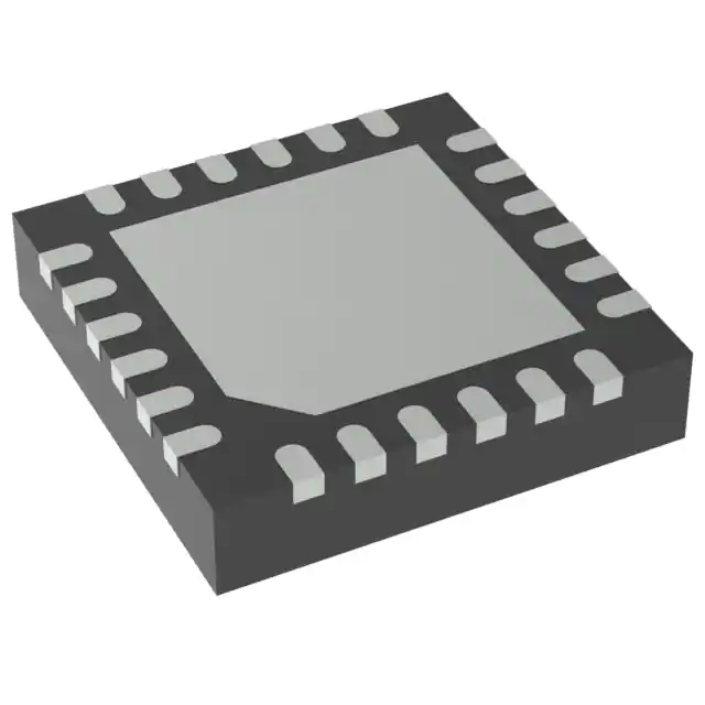


 工商网监
湘ICP备2023018690号
工商网监
湘ICP备2023018690号

