Product
Folder
Order
Now
Support &
Community
Tools &
Software
Technical
Documents
bq25703A
SLUSCU1A – MAY 2017 – REVISED MAY 2018
bq25703A I2C Multi-Chemistry Battery Buck-Boost Charge Controller With System Power
Monitor and Processor Hot Monitor
•
•
•
•
•
•
•
•
•
Charge 1- to 4-Cell Battery From Wide Range of
Input Sources
– 3.5-V to 24-V Input Operating Voltage
– Supports USB2.0, USB 3.0, USB 3.1 (Type C),
and USB_PD Input Current Settings
– Seamless Transition Between Buck and Boost
Operation
– Input Current and Voltage Regulation (IDPM
and VDPM) Against Source Overload
Power/Current Monitor for CPU Throttling
– Comprehensive PROCHOT Profile, IMVP8
Compliant
– Input and Battery Current Monitor
– System Power Monitor, IMVP8 Compliant
Narrow-VDC (NVDC) Power Path Management
– Instant-On With No Battery or Deeply
Discharged Battery
– Battery Supplements System When Adapter is
Fully-Loaded
Power Up USB Port From Battery (USB OTG)
– Output 4.48-V to 20.8-V Compatible With USB
PD
– Output Current Limit up to 6.35 A
800-kHz or 1.2-MHz Programmable Switching
Frequency for 1-µH to 3.3-µH Inductor
Host Control Interface for Flexible System
Configuration
– I2C (bq25703A) Port for Optimal System
Performance and Status Reporting
– Hardware Pin to Set Input Current Limit
Without EC Control
Integrated ADC to Monitor Voltage, Current and
Power
High Accuracy Regulation and Monitor
– ±0.5% Charge Voltage Regulation
– ±2% Input/Charge Current Regulation
– ±2% Input/Charge Current Monitor
– ±5% Power Monitor
Safety
– Thermal Shutdown
– Input, System, Battery Overvoltage Protection
– MOSFET Inductor Overcurrent Protection
Low Battery Quiescent Current
•
•
Input Current Optimizer (ICO) to Extract Max Input
Power
Charge Any Battery Chemistry: Li+, LiFePO4,
NiCd, NiMH, Lead Acid
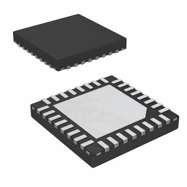
Package: 32-Pin 4 × 4 WQFN
2 Applications
•
•
•
Drones, Bluetooth Speakers, IP Cameras,
Detachable, Tablet PCs and Power Bank
Industrial and Medical Equipment
Portable Equipment With Rechargeable Batteries
3 Description
The bq25703A is a synchronous NVDC battery buckboost charge controller, offering low component
count, high efficiency solution for space-constraint,
multi-chemistry battery charging applications.
The NVDC-1 configuration allows the system to be
regulated at battery voltage, but not drop below
system minimum voltage. The system keeps
operating even when the battery is completely
discharged or removed. When load power exceeds
input source rating, the battery goes into supplement
mode and prevents the system from crashing.
The bq25703A charges battery from a wide range of
input sources including USB adapter, high voltage
USB PD sources and traditional adapters.
Device Information
PART NUMBER
PACKAGE
bq25703A
(1)
BODY SIZE (NOM)
WQFN (32)
4.00 mm × 4.00 mm
(1) For all available packages, see the orderable addendum at
the end of the data sheet.
Application Diagram
VSYS
Adapter
3.5V ± 24V
BATT
(1S-4S)
Q1
Q2
Q3
Q4
HIDRV1
SW1BTST1BTST2SW2
HIDRV2
LODRV1
LODRV2 SYS
VBUS
ACN
/BATDRV
bq25703A
ACP
SRP
SRN
IADPT, IBAT,
PSYS, PROCHOT
•
1
•
I2C
1 Features
Host
(703A I2C)
Copyright © 2017, Texas Instruments Incorporated
1
An IMPORTANT NOTICE at the end of this data sheet addresses availability, warranty, changes, use in safety-critical applications,
intellectual property matters and other important disclaimers. PRODUCTION DATA.
�bq25703A
SLUSCU1A – MAY 2017 – REVISED MAY 2018
www.ti.com
Table of Contents
1
2
3
4
5
6
7
Features ..................................................................
Applications ...........................................................
Description .............................................................
Revision History.....................................................
Description (continued).........................................
Pin Configuration and Functions .........................
Specifications.........................................................
7.1
7.2
7.3
7.4
7.5
7.6
7.7
8
1
1
1
2
5
6
9
Absolute Maximum Ratings ...................................... 9
ESD Ratings ............................................................ 9
Recommended Operating Conditions....................... 9
Thermal Information ................................................ 10
Electrical Characteristics......................................... 10
Timing Requirements .............................................. 18
Typical Characteristics ........................................... 19
Detailed Description ............................................ 22
8.1
8.2
8.3
8.4
Overview ................................................................
Functional Block Diagram ......................................
Feature Description.................................................
Device Functional Modes........................................
22
23
24
30
8.5 Programming .......................................................... 31
8.6 Register Map........................................................... 34
9
Application and Implementation ........................ 68
9.1 Application Information .......................................... 68
9.2 Typical Application .................................................. 68
10 Power Supply Recommendations ..................... 75
11 Layout................................................................... 76
11.1 Layout Guidelines ................................................. 76
11.2 Layout Example .................................................... 76
12 Device and Documentation Support ................. 78
12.1
12.2
12.3
12.4
12.5
12.6
12.7
Device Support ....................................................
Documentation Support .......................................
Receiving Notification of Documentation Updates
Community Resources..........................................
Trademarks ...........................................................
Electrostatic Discharge Caution ............................
Glossary ................................................................
78
78
78
78
78
78
78
13 Mechanical, Packaging, and Orderable
Information ........................................................... 79
13.1 Package Option Addendum .................................. 80
4 Revision History
NOTE: Page numbers for previous revisions may differ from page numbers in the current version.
Changes from Original (May 2017) to Revision A
Page
•
Deleted Ideal Diode Operation in Supplement Mode from Features ..................................................................................... 1
•
Changed 2.2-µH to 3.3-µH and deleted Low Profile in Features .......................................................................................... 1
•
Added Integrated ADC to Monitor Voltage, Current and Power to Features ......................................................................... 1
•
Added Detachable, Tablet PCs and Power Bank to Applications .......................................................................................... 1
•
Changed input source from being overloaded to system from crashing in Description ......................................................... 1
•
Changed 703 I2C to 703A I2C in Application Diagram .......................................................................................................... 1
•
Changed 18.5 V for 3-cell to 19.5 V for 3-cell and 4-cell in CELL_BATPRESZ description .................................................. 6
•
Changed I to O for CMPOUT I/O ........................................................................................................................................... 7
•
Changed V(IADP) to V(IADPT) in IADPT description ................................................................................................................... 7
•
Deleted minimum 10-ms and added minimum to PROCHOT description ............................................................................ 7
•
Changed 10-Ω to 10-mΩ in IDPM_REG_ACC in Electrical Characteristics ................................................................................. 11
•
Changed 10-Ω to 10-mΩ for IDPM_REG_ACC_ILIM in Electrical Characteristics ......................................................................... 11
•
Changed REG0x07/06 to REG0x0B/0A in VDPM_REG_ACC Test Conditions in Electrical Characteristics .............................. 12
•
Changed REG0x0B/0A to REG0x07/06 in VOTG_REG_ACC Test Conditions in Electrical Characteristics .............................. 12
•
Changed REG0x01[7] = 0 to REG0x01[7] = 1 in Test Conditions for IBAT_BATFET_ON ............................................................ 12
•
Changed IBATOVP test condition from: on SRP and SRN to: on VSYS pin............................................................................ 15
•
Changed Q3 to ACX in CONVERTER OVER-CURRENT COMPARATOR (ACX) in Electrical Characteristics ................ 16
•
Added overbar to (BATDRV) in heading ............................................................................................................................. 17
•
Added overbar to PROCHOT in Overview .......................................................................................................................... 22
•
Changed After CHRG_OK goes HIGH to When CHRG_OK goes LOW in Input Voltage and Current Limit Setup............ 24
•
Changed Table 1 ................................................................................................................................................................. 24
•
Changed 19.5 to 19.5V in 3S row SYSOVP column in Table 1 .......................................................................................... 24
•
Changed 0 to 0 A, lowside to low-side, and LSFET turn-on to LSFET turn-on when the HSFET is off in Continuous
Conduction Mode (CCM) ..................................................................................................................................................... 25
2
Submit Documentation Feedback
Copyright © 2017–2018, Texas Instruments Incorporated
�bq25703A
www.ti.com
SLUSCU1A – MAY 2017 – REVISED MAY 2018
Revision History (continued)
•
Changed Pulse Frequency Modulation (PFM) .................................................................................................................... 25
•
Changed during forward mode to during forward supplement mode in High-Accuracy Current Sense Amplifier
(IADPT and IBAT)................................................................................................................................................................. 26
•
Changed REG0x33[5] to REG0x33[5](EN_PKPWR_IDPM) or REG0x33[4](EN_PKPWR_VSYS) in Two-Level
Adapter Current Limit (Peak Power Mode) .......................................................................................................................... 26
•
Added last sentence to Two-Level Adapter Current Limit (Peak Power Mode) .................................................................. 26
•
Changed Processor Hot Indication ...................................................................................................................................... 27
•
Changed IADP to IADPT in Figure 13.................................................................................................................................. 28
•
Changed bq2570x to bq2570xA in Figure 14 ...................................................................................................................... 29
•
Added overbar to PROCHOT in PROCHOT Status ............................................................................................................ 29
•
Changed subscript of ILIM2_VTH in Input Overcurrent Protection (ACOC) .............................................................................. 29
•
Changed bq25700 to bq25703A and 3s – 18.5 V to 3s/4s – 19.5 V in System Overvoltage Protection (SYSOVP)........... 30
•
Added REG to Battery Charging ......................................................................................................................................... 30
•
Changed The SMBUS address is 12h (0001001_X), where X is the read/write bit. to The I2C address is D6h
(1101101_X), where X is the read/write bit. in Programming .............................................................................................. 31
•
Added h suffix to addresses in ADDR column in Table 4 ................................................................................................... 34
•
Changed 0 mA – 6350 mA to 50 mA – 6400 mA for 0F/0Eh in Table 4 ............................................................................. 35
•
Changed Device Address to DeviceID for 2Fh in Table 4 .................................................................................................. 35
•
Changed I2C address from 01h/00h to 01/00h in Figure 23 ............................................................................................... 36
•
Changed bit numbers from 15-8 to 7-0 in Figure 23 ........................................................................................................... 36
•
Added to PWM_FREQ description in Table 5 ........................................................................................ 37
•
Added sentence to IBAT_GAIN description in Table 6 ....................................................................................................... 37
•
Changed LDO to internal resistor in EN_LDO description in Table 6 ................................................................................. 37
•
Changed I2C address from 31h/30h to 31/30h in ChargeOption1 Register (I2C address = 31/30h) [reset = 211h] .......... 38
•
Changed bit numbers from 15-8 to 7-0 in Figure 24 ........................................................................................................... 38
•
Deleted Independent Comparator Reference in Table 8 .................................................................................................... 38
•
Changed 2.4 V and 1.3 V to 2.3 V and 1.2 V for CMP_REF in Table 8 .............................................................................. 38
•
Deleted Independent Comparator Polarity in Table 8 ......................................................................................................... 39
•
Deleted Independent Comparator Deglitch Time in Table 8 ............................................................................................... 39
•
Added independent to FORCE_LATCHOFF description in Table 8 ................................................................................... 39
•
Changed I2C address from 33h/32h to 33/32h in ChargeOption2 Register (I2C address = 33/32h) [reset = 2B7] ........... 40
•
Changed bit numbers from 15-8 to 7-0 in Figure 25 ........................................................................................................... 40
•
Changed I2C address from 35h/34h to 35/34h in ChargeOption3 Register (I2C address = 35/34h) [reset = 0h] .............. 42
•
Changed bit numbers from 15-8 to 7-0 in Figure 26 ........................................................................................................... 42
•
Added to BATFETOFF_ HIZ description in Table 12 ............................................................................. 42
•
Added to PSYS_OTG_ IDCHG description in Table 12 ......................................................................... 42
•
Changed I2C address from 37h/36h to 37/36h in ChargeOption3 Register (I2C address = 35/34h) [reset = 0h] .............. 43
•
Changed bit numbers from 15-11 to 7-3, 10-9 to 2-1, 8 to 0 in Figure 27 .......................................................................... 43
•
Added PROCHOT Pulse Extension Enable to EN_PROCHOT_EXT description in Table 14 ............................................ 43
•
Changed I2C address from 39h/38h to 39/38h in ProchotOption1 Register (I2C address = 39/38h) [reset = 8120h] ....... 45
•
Changed bit numbers from 15-10 to 7-2, 9-8 to 1-0 in Figure 28 ....................................................................................... 45
•
Added There is a 128 mA offset. to IDCHG_VTH description in Table 15 .......................................................................... 45
•
Changed 0 mA to 000000b in IDCHG_VTH description in Table 15 ................................................................................... 45
•
Changed PROCHOT_PROFILE_ACOK description in Table 16 ......................................................................................... 46
•
Changed bit numbers from 15 to 7, 14 to 6, 13 to 5 and 12-8 to 4-0 in Figure 29 ............................................................. 47
•
Changed bit numbers from 15-8 to 7-0 in Figure 30 ........................................................................................................... 49
Copyright © 2017–2018, Texas Instruments Incorporated
Submit Documentation Feedback
3
�bq25703A
SLUSCU1A – MAY 2017 – REVISED MAY 2018
www.ti.com
Revision History (continued)
•
Changed bit numbers from 15-8 to 7-0 in Figure 31 ........................................................................................................... 51
•
Changed text in ChargeCurrent Register (I2C address = 03/02h) [reset = 0h] ................................................................... 52
•
Changed bit numbers from 15-8 to 7-0 in Figure 32 ........................................................................................................... 52
•
Deleted Upon POR or when charge is disabled, the system is regulated at the MaxChargeVoltage register. from
MaxChargeVoltage Register (I2C address = 05/04h) [reset value based on CELL_BATPRESZ pin setting] .................... 54
•
Changed bit numbers from 15-8 to 7-0 in Figure 33 ........................................................................................................... 54
•
Changed bit numbers from 15-8 to 7-0 in Figure 34 ........................................................................................................... 56
•
Deleted text and changed larger to 20-mΩ in Input Current Registers ............................................................................... 57
•
Added paragraph to IIN_HOST Register With 10-mΩ Sense Resistor (I2C address = 0F/0Eh) [reset = 4000h]................ 58
•
Changed bit numbers from 15-8 to 7-0 in Figure 35 ........................................................................................................... 58
•
Changed bit numbers from 15-8 to 7-0 in Figure 36 ........................................................................................................... 59
•
Changed bit numbers from 15-8 to 7-0 in Figure 37 ........................................................................................................... 60
•
Changed bit numbers from 15-8 to 7-0 in Figure 38 ........................................................................................................... 61
•
Changed bit numbers from 15-8 to 7-0 in Figure 39 ........................................................................................................... 62
•
Changed I2C address to 27/26h in ADCVBUS/PSYS Register (I2C address = 27/26h) .................................................... 63
•
Changed bit numbers from 15-8 to 7-0 in Figure 40 ........................................................................................................... 63
•
Changed ADCVBUS/PSYS Register Field Descriptions into two tables.............................................................................. 63
•
Changed I2C address to 29/28h in ADCIBAT Register (I2C address = 29/28h) ................................................................ 64
•
Changed bit numbers from 15-8 to 7-0 in Figure 41 ........................................................................................................... 64
•
Changed ADCIBAT Register Field Descriptions into two tables .......................................................................................... 64
•
Changed I2C address to 2B/2Ah in ADCIINCMPIN Register (I2C address = 2B/2Ah) ...................................................... 65
•
Changed bit numbers from 15-8 to 7-0 in Figure 42 ........................................................................................................... 65
•
Changed ADCIINCMPIN Register Field Descriptions into two tables .................................................................................. 65
•
Changed I2C address to 2D/2Ch in ADCVSYSVBAT Register (I2C address = 2D/2Ch) ................................................... 66
•
Changed bit numbers from 15-8 to 7-0 in Figure 43 ........................................................................................................... 66
•
Changed ADCVSYSVBAT Register Field Descriptions into two tables ............................................................................... 66
•
Changed bit numbers from 15-8 to 7-0 in Figure 44 ........................................................................................................... 67
•
Deleted 15-8, Reserved, and R from Figure 45 .................................................................................................................. 67
•
Deleted 15-8, Reserved, and R from Table 48 ................................................................................................................... 67
•
Changed Figure 46 .............................................................................................................................................................. 68
•
Changed Minimum System Voltage from 614 mV to 6144 mV in Design Requirements .................................................... 69
•
Deleted Input Snubber and Filter for Voltage Spike Damping section ................................................................................ 69
•
Changed Figure 47 .............................................................................................................................................................. 69
•
Added Bulk input capacitors should be locate in front of input current sensing resistor. Do not recommend to put
bulk input capacitors between input sensing resistor and switching MOSFET. to Input Capacitor .................................... 70
•
Changed Minimum 4 - 6 pcs of 10-µF 0805 size capacitor is suggested for 45 - 65 W adapter design. to Minimum
10-µF effective capacitance (7 pcs of 10-µF 0805 size capacitor) is suggested for 45 W-65 W adapter. in Input
Capacitor .............................................................................................................................................................................. 70
•
Changed Minimum 6 pcs of 10-µF 0805 size capacitor is suggested to be placed by the inductor. to Minimum 10-µF
effective capacitance (7 pcs of 10-µF 0805 size capacitor) is suggested to be placed by the inductor, and 50-µF
effective distributed capacitance on Vsys output. in Output Capacitor ................................................................................ 70
4
Submit Documentation Feedback
Copyright © 2017–2018, Texas Instruments Incorporated
�bq25703A
www.ti.com
SLUSCU1A – MAY 2017 – REVISED MAY 2018
5 Description (continued)
During power up, the charger sets converter to buck, boost or buck-boost configuration based on input source
and battery conditions. The charger automatically transits among buck, boost and buck-boost configuration
without host control.
In the absence of an input source, the bq25703A supports On-the-Go (OTG) function from 1- to 4-cell battery to
generate 4.48 V to 20.8 V on VBUS. During OTG mode, the charger regulates output voltage and output current.
The bq25703A monitors adapter current, battery current and system power. The flexibly programmed PROCHOT
output goes directly to CPU for throttle back when needed.
Copyright © 2017–2018, Texas Instruments Incorporated
Submit Documentation Feedback
5
�bq25703A
SLUSCU1A – MAY 2017 – REVISED MAY 2018
www.ti.com
6 Pin Configuration and Functions
SW1
HIDRV1
BTST1
LODRV1
REGN
PGND
LODRV2
BTST2
32
31
30
29
28
27
26
25
RSN Package
32-Pin WQFN
Top View
VBUS
1
24
HIDRV2
ACN
2
23
SW2
ACP
3
22
VSYS
CHRG_OK
4
21
BATDRV
EN_OTG
5
20
SRP
ILIM_HIZ
6
19
SRN
VDDA
7
18
CELL_BATPRESZ
IADPT
8
17
COMP2
Thermal
13
14
15
16
SCL
CMPIN
CMPOUT
COMP1
11
PROCHOT
12
10
PSYS
SDA
9
IBAT
Pad
Pin Functions
PIN
NAME
NUMBER
I/O
DESCRIPTION
ACN
2
PWR
Input current sense resistor negative input. The leakage on ACP and ACN are matched. The
series resistors on the ACP and ACN pins are placed between sense resistor and filter cap.
Refer to Application and Implementation for ACP/ACN filter design.
ACP
3
PWR
Input current sense resistor positive input. The leakage on ACP and ACN are matched. The
series resistors on the ACP and ACN pins are placed between sense resistor and filter cap.
Refer to Application and Implementation for ACP/ACN filter design.
BATDRV
21
O
P-channel battery FET (BATFET) gate driver output. It is shorted to VSYS to turn off the
BATFET. It goes 10 V below VSYS to fully turn on BATFET. BATFET is in linear mode to
regulate VSYS at minimum system voltage when battery is depleted. BATFET is fully on
during fast charge and supplement mode.
BTST1
30
PWR
Buck mode high side power MOSFET driver power supply. Connect a 0.047-µF capacitor
between SW1 and BTST1. The bootstrap diode between REGN and BTST1 is integrated.
BTST2
25
PWR
Boost mode high side power MOSFET driver power supply. Connect a 0.047-μF capacitor
between SW2 and BTST2. The bootstrap diode between REGN and BTST2 is integrated.
CELL_BATPRESZ
6
18
I
Submit Documentation Feedback
Battery cell selection pin for 1–4 cell battery setting. CELL_BATPRESZ pin is biased from
VDDA. CELL_BATPRESZ pin also sets SYSOVP threshold to 5 V for 1-cell, 12 V for 2-cell,
and 19.5 V for 3-cell/4-cell. CELL_BATPRESZ pin is pulled below VCELL_BATPRESZ_FALL to
indicate battery removal. The device exits LEARN mode, and disables charge.
REG0x05/04() goes back to default.
Copyright © 2017–2018, Texas Instruments Incorporated
�bq25703A
www.ti.com
SLUSCU1A – MAY 2017 – REVISED MAY 2018
Pin Functions (continued)
PIN
NAME
CHRG_OK
NUMBER
4
I/O
DESCRIPTION
O
Open drain active high indicator to inform the system good power source is connected to the
charger input. Connect to the pullup rail via 10-kΩ resistor. When VBUS rises above 3.5V or
falls below 24.5V, CHRG_OK is HIGH after 50ms deglitch time. When VBUS is falls below
3.2 V or rises above 26 V, CHRG_OK is LOW. When fault occurs, CHRG_OK is asserted
LOW.
CMPIN
14
I
Input of independent comparator. The independent comparator compares the voltage sensed
on CMPIN pin to internal reference, and its output is on CMPOUT pin. Internal reference,
output polarity and deglitch time is selectable by I2C. With polarity HIGH (REG0x30[6] = 1),
place a resistor between CMPIN and CMPOUT to program hysteresis. With polarity LOW
(REG0x30[6] = 0), the internal hysteresis is 100 mV. If the independent comparator is not in
use, tie CMPIN to ground.
CMPOUT
15
O
Open-drain output of independent comparator. Place pullup resistor from CMPOUT to pullup
supply rail. Internal reference, output polarity and deglitch time are selectable by I2C.
COMP2
17
I
Buck boost converter compensation pin 2. Refer to bq25700 EVM schematic for COMP2 pin
RC network.
COMP1
16
I
Buck boost converter compensation pin 1. Refer to bq25700 EVM schematic for COMP1 pin
RC network.
EN_OTG
5
I
Active HIGH to enable OTG mode. When EN_OTG pin is HIGH and REG0x35[4] is HIGH,
OTG can be enabled, refer to USB On-The-Go (OTG) for details of how to enable OTG
function
HIDRV1
31
O
Buck mode high side power MOSFET (Q1) driver. Connect to high side n-channel MOSFET
gate.
HIDRV2
24
O
Boost mode high side power MOSFET(Q4) driver. Connect to high side n-channel MOSFET
gate.
I/O
Buffered adapter current output. V(IADPT) = 20 or 40 × (V(ACP) – V(ACN)). With ratio selectable
in REG0x00[4]. Place a resistor from the IADPT pin to ground corresponding to inductor in
use. For 2.2 µH, the resistor is 137 kΩ. Place 100-pF or less ceramic decoupling capacitor
from IADPT pin to ground. IADPT output voltage is clamped below 3.3 V.
O
Buffered battery current selected by I2C. V(IBAT) = 8 or 16 × (V(SRP) – V(SRN)) for charge
current, or V(IBAT) = 8 or 16 × (V(SRN) – V(SRP)) for discharge current, with ratio selectable in
REG0x00[3]. Place 100-pF or less ceramic decoupling capacitor from IBAT pin to ground.
This pin can be floating if not in use. Its output voltage is clamped below 3.3 V.
IADPT
IBAT
8
9
ILIM_HIZ
6
I
Input current limit input. Program ILIM_HIZ voltage by connecting a resistor divider from
supply rail to ILIM_HIZ pin to ground. The pin voltage is calculated as: V(ILIM_HIZ) = 1 V + 40
× IDPM × RAC, in which IDPM is the target input current. The input current limit used by the
charger is the lower setting of ILIM_HIZ pin and REG0x0F() and REG0x0E(). When the pin
voltage is below 0.4 V, the device enters Hi-Z mode with low quiescent current. When the pin
voltage is above 0.8 V, the device is out of Hi-Z mode.
LODRV1
29
O
Buck mode low side power MOSFET (Q2) driver. Connect to low side n-channel MOSFET
gate.
LODRV2
26
O
Boost mode low side power MOSFET (Q3) driver. Connect to low side n-channel MOSFET
gate.
PGND
27
GND
PROCHOT
11
O
Active low open drain output of processor hot indicator. It monitors adapter input current,
battery discharge current, and system voltage. After any event in the PROCHOT profile is
triggered, a pulse is asserted. The minimum pulse width is adjustable in REG0x36[5:2].
PSYS
10
O
Current mode system power monitor. The output current is proportional to the total power
from the adapter and battery. The gain is selectable through I2C. Place a resistor from PSYS
to ground to generate output voltage. This pin can be floating if not in use. Its output voltage
is clamped below 3.3 V. Place a capacitor in parallel with the resistor for filtering.
REGN
28
PWR
SCL
13
I
SDA
12
I/O
Device power ground.
6-V linear regulator output supplied from VBUS or VSYS. The LDO is active when VBUS
above VVBUS_CONVEN. Connect a 2.2- or 3.3-μF ceramic capacitor from REGN to power
ground. REGN pin output is for power stage gate drive.
I2C clock input. Connect to clock line from the host controller or smart battery. Connect a 10kΩ pullup resistor according to I2C specifications.
I2C open-drain data I/O. Connect to data line from the host controller or smart battery.
Connect a 10-kΩ pullup resistor according to I2C specifications.
Copyright © 2017–2018, Texas Instruments Incorporated
Submit Documentation Feedback
7
�bq25703A
SLUSCU1A – MAY 2017 – REVISED MAY 2018
www.ti.com
Pin Functions (continued)
PIN
NAME
SRN
NUMBER
19
I/O
DESCRIPTION
PWR
Charge current sense resistor negative input. SRN pin is for battery voltage sensing as well.
Connect SRN pin with optional 0.1-μF ceramic capacitor to GND for common-mode filtering.
Connect a 0.1-μF ceramic capacitor from SRP to SRN to provide differential mode filtering.
The leakage current on SRP and SRN are matched. For reverse battery plug-in protection,
10-Ω series resistors are placed on SRP and SRN.
SRP
20
PWR
Charge current sense resistor positive input. Connect 0.1-μF ceramic capacitor from SRP to
SRN to provide differential mode filtering. The leakage current on SRP and SRN are
matched. For reverse battery plug-in protection, 10-Ω series resistors are placed on SRP and
SRN. Connect SRP pin with optional 0.1-uF ceramic capacitor to GND for common-mode
filtering.
SW1
32
PWR
Buck mode high side power MOSFET driver source. Connect to the source of the high side
n-channel MOSFET.
SW2
23
PWR
Boost mode high side power MOSFET driver source. Connect to the source of the high side
n-channel MOSFET.
VBUS
1
PWR
Charger input voltage. An input low pass filter of 1Ω and 0.47 µF (minimum) is
recommended.
VDDA
7
PWR
Internal reference bias pin. Connect a 10-Ω resistor from REGN to VDDA and a 1-μF
ceramic capacitor from VDDA to power ground.
VSYS
22
PWR
Charger system voltage sensing. The system voltage regulation limit is programmed in
REG0x05/04() and REG0X0D/0C().
Thermal pad
–
–
8
Submit Documentation Feedback
Exposed pad beneath the IC. Analog ground and power ground star-connected near the IC's
ground. Always solder thermal pad to the board, and have vias on the thermal pad plane
connecting to power ground planes. It also serves as a thermal pad to dissipate the heat.
Copyright © 2017–2018, Texas Instruments Incorporated
�bq25703A
www.ti.com
SLUSCU1A – MAY 2017 – REVISED MAY 2018
7 Specifications
7.1 Absolute Maximum Ratings
over operating free-air temperature range (unless otherwise noted) (1) (2)
MIN
MAX
SRN, SRP, ACN, ACP, VBUS, VSYS, BATDRV
–0.3
30
SW1, SW2
–2.0
30
BTST1, BTST2, HIDRV1, HIDRV2
–0.3
36
LODRV1, LODRV2 (2% duty cycle)
–4.0
7
HIDRV1, HIDRV2 (2% duty cycle)
–4.0
36
SW1, SW2 (2% duty cycle)
–4.0
30
SDA, SCL, REGN, CHRG_OK, CELL_BATPRESZ,
ILIM_HIZ, LODRV1, LODRV2, VDDA, COMP1, COMP2,
CMPIN, CMPOUT, EN_OTG
–0.3
7
PROCHOT
–0.3
5.5
IADPT, IBAT, PSYS
–0.3
3.6
BTST1-SW1, BTST2-SW2, HIDRV1-SW1, HIDRV2-SW2
–0.3
7
SRP-SRN, ACP-ACN
–0.5
0.5
Junction temperature range, TJ
–40
155
°C
Storage temperature, Tstg
–40
155
°C
Voltage
Differential voltage
(1)
(2)
UNIT
V
V
Stresses beyond those listed under Absolute Maximum Ratings may cause permanent damage to the device. These are stress ratings
only, which do not imply functional operation of the device at these or any other conditions beyond those indicated under Recommended
Operating Conditions. Exposure to absolute-maximum-rated conditions for extended periods may affect device reliability.
All voltages are with respect to GND if not specified. Currents are positive into, negative out of the specified terminal. Consult Packaging
Section of the data book for thermal limitations and considerations of packages.
7.2 ESD Ratings
VALUE
V(ESD)
(1)
(2)
Electrostatic discharge
Human-body model (HBM), per ANSI/ESDA/JEDEC JS-001 (1)
±2000
Charged-device model (CDM), per JEDEC specification JESD22-C101 (2)
±500
UNIT
V
JEDEC document JEP155 states that 500-V HBM allows safe manufacturing with a standard ESD control process.
JEDEC document JEP157 states that 250-V CDM allows safe manufacturing with a standard ESD control process.
7.3 Recommended Operating Conditions
over operating free-air temperature range (unless otherwise noted)
MIN
MAX
UNIT
ACN, ACP, VBUS
0
24
SRN, SRP, VSYS, BATDRV
0
19.2
–2
24
BTST1, BTST2, HIDRV1, HIDRV2
0
30
SDA, SCL, REGN, CHRG_OK, CELL_BATPRESZ, ILIM_HIZ, LODRV1,
LODRV2, VDDA, COMP1, COMP2, CMPIN, CMPOUT
0
6.5
PROCHOT
0
5.3
IADPT, IBAT, PSYS
0
3.3
BTST1-SW1, BTST2-SW2, HIDRV1-SW1, HIDRV2-SW2
0
6.5
–0.35
0.35
Junction temperature, TJ
–40
125
°C
Operating free-air temperature, TA
–40
85
°C
SW1, SW2
Voltage
Differential
voltage
SRP-SRN, ACP-ACN
Copyright © 2017–2018, Texas Instruments Incorporated
V
V
Submit Documentation Feedback
9
�bq25703A
SLUSCU1A – MAY 2017 – REVISED MAY 2018
www.ti.com
7.4 Thermal Information
bq25703A
THERMAL METRIC (1)
RSN (WQFN)
UNIT
32 PINS
RθJA
Junction-to-ambient thermal resistance
37.2
°C/W
RθJC(top)
Junction-to-case (top) thermal resistance
26.1
°C/W
RθJB
Junction-to-board thermal resistance
7.8
°C/W
ψJT
Junction-to-top characterization parameter
0.3
°C/W
ψJB
Junction-to-board characterization parameter
7.8
°C/W
RθJC(bot)
Junction-to-case (bottom) thermal resistance
2.3
°C/W
(1)
For more information about traditional and new thermal metrics, see the Semiconductor and IC Package Thermal Metrics application
report.
7.5 Electrical Characteristics
over TJ = –40 to 125°C (unless otherwise noted)
PARAMETER
VINPUT_OP
TEST CONDITIONS
Input voltage operating range
MIN
TYP
MAX
UNIT
3.5
26
V
1.024
19.2
V
REGULATION ACCURACY
MAX SYSTEM VOLTAGE REGULATION
VSYSMAX_RNG
System voltage regulation,
measured on VSYS
REG0x05/04() = 0x41A0H
(16.800 V)
VSYSMAX_ACC
System voltage regulation
accuracy (charge disable)
REG0x05/04() = 0x3130H
(12.592 V)
VSRN + 160 mV
–2%
V
2%
VSRN + 160 mV
–2%
V
2%
VSRN + 160 mV
V
REG0x05/04() = 0x20D0H
(8.400 V)
–3%
REG0x05/04() = 0x1060H
(4.192 V)
–3%
3%
1.024
19.2
3%
VSRN + 160 mV
V
MINIMUM SYSTEM VOLTAGE REGULATION
VSYSMIN_RNG
System voltage regulation,
measured on VSYS
REG0x0D/0C() = 0x3000H
VSYSMIN_REG_ACC
Minimum system voltage
regulation accuracy (charge
enable, VBAT below
REG0x0D/0C() setting)
REG0x0D/0C() = 0x2400H
REG0x0D/0C() = 0x1800H
REG0x0D/0C() = 0x0E00H
12.288
–2%
V
V
2%
9.216
–2%
V
2%
6.144
–3%
V
3%
3.584
–3%
V
4%
CHARGE VOLTAGE REGULATION
VBAT_RNG
Battery voltage regulation
1.024
REG0x05/04() = 0x41A0H
VBAT_REG_ACC
Battery voltage regulation
accuracy (charge enable)
(0°C to 85°C)
REG0x05/04() = 0x3130H
REG0x05/04() = 0x20D0H
REG0x05/04() = 0x1060H
10
Submit Documentation Feedback
19.2
16.8
–0.5%
V
0.5%
12.592
–0.5%
V
0.5%
8.4
–0.6%
V
0.6%
4.192
–1.1%
V
V
1.2%
Copyright © 2017–2018, Texas Instruments Incorporated
�bq25703A
www.ti.com
SLUSCU1A – MAY 2017 – REVISED MAY 2018
Electrical Characteristics (continued)
over TJ = –40 to 125°C (unless otherwise noted)
PARAMETER
TEST CONDITIONS
MIN
TYP
MAX
UNIT
81.28
mV
CHARGE CURRENT REGULATION IN FAST CHARGE
VIREG_CHG_RNG
Charge current regulation
differential voltage range
VIREG_CHG = VSRP –
VSRN
REG0x03/02() = 0x1000H
ICHRG_REG_ACC
Charge current regulation
REG0x03/02() = 0x0800H
accuracy 10-mΩ current
sensing resistor, VBAT above
0x0D/0C() setting (0°C to
REG0x03/02() = 0x0400H
85°C)
REG0x03/02() = 0x0200H
0
4096
–3%
mA
2%
2048
–4%
mA
3%
1024
–5%
mA
6%
512
–12%
mA
12%
CHARGE CURRENT REGULATION IN LDO MODE
ICLAMP
Pre-charge current clamp
CELL 2s-4s
384
mA
CELL 1 s, VSRN < 3 V
384
mA
CELL 1 s, 3 V < VSRN <
VSYSMIN
2
REG0x03/02() = 0x0180H
384
2S-4S
–15%
1S
–25%
REG0x03/02() = 0x0100H
IPRECHRG_REG_ACC
Pre-charge current regulation
2S-4S
accuracy with 10-Ω SRP/SRN
series resistor, VBAT below
1S
REG0x0D/0C() setting (0°C to
REG0x03/02() = 0x00C0H
85°C)
2S-4S
1S
ILEAK_SRP_SRN
mA
15%
25%
256
–20%
mA
20%
–35%
35%
192
–25%
mA
25%
–50%
REG0x03/02() = 0x0080H
2S-4S
A
50%
128
mA
–30%
30%
–12
10
µA
0.5
64
mV
REG0x0F/0E() = 0x4FFFH
3820
4000
mA
REG0x0F/0E() = 0x3BFFH
2830
3000
mA
REG0x0F/0E() = 0x1DFFH
1350
1500
mA
REG0x0F/0E() = 0x09FFH
340
500
mA
–16
10
µA
1
4
V
SRP, SRN leakage current
mismatch (0°C to 85°C)
INPUT CURRENT REGULATION
VIREG_DPM_RNG
Input current regulation
differential voltage range
IDPM_REG_ACC
Input current regulation
accuracy (–40°C to 105°C)
with 10-mΩ ACP/ACN series
resistor
VIREG_DPM = VACP – VACN
ILEAK_ACP_ACN
ACP, ACN leakage current
mismatch
VIREG_DPM_RNG_ILIM
Voltage Range for input
current regulation
IDPM_REG_ACC_ILIM
VILIM_HIZ = 2.6 V
Input Current Regulation
Accuracy on ILIM_HIZ pin
VILIM_HIZ = 2.2 V
VILIM_HIZ = 1 V + 40 × IDPM ×
VILIM_HIZ = 1.6 V
RAC with 10-mΩ ACP/ACN
series resistor
VILIM_HIZ = 1.2 V
ILEAK_ILIM
ILIM_HIZ pin leakage
3800
4000
4200
mA
2800
3000
3200
mA
1300
1500
1700
mA
300
500
700
mA
–1
1
µA
3.2
19.52
V
INPUT VOLTAGE REGULATION
VIREG_DPM_RNG
Input voltage regulation range Voltage on VBUS
Copyright © 2017–2018, Texas Instruments Incorporated
Submit Documentation Feedback
11
�bq25703A
SLUSCU1A – MAY 2017 – REVISED MAY 2018
www.ti.com
Electrical Characteristics (continued)
over TJ = –40 to 125°C (unless otherwise noted)
PARAMETER
TEST CONDITIONS
MIN
REG0x0B/0A()=0x3C80H
TYP
18688
–2%
VDPM_REG_ACC
Input voltage regulation
accuracy
MAX
REG0x0B/0A()=0x1E00H
mV
2%
10880
–2.5%
REG0x0B/0A()=0x0500H
UNIT
mV
2.5%
4480
mV
–3%
5%
0
81.28
mV
OTG CURRENT REGULATION
VIOTG_REG_RNG
Input current regulation
differential voltage range
IOTG_ACC
Input current regulation
accuracy with 50-mA LSB,
with 10-Ω ACP/ACN series
resistor
VIREG_DPM = VACP – VACN
REG0x09/08() = 0x3C00H
2800
3000
3200
mA
REG0x09/08() = 0x1E00H
1300
1500
1700
mA
REG0x09/08() = 0x0A00H
300
500
700
mA
20.8
V
OTG VOLTAGE REGULATION
VIREG_DPM_RNG
Input voltage regulation range Voltage on VBUS
REG0x07/06()=0x3CC0H
VOTG_REG_ACC
OTG voltage regulation
accuracy
REG0x07/06()=0x1D80H
REG0x07/06()=0x0240H
4.48
20.032
–2%
V
2%
12.032
–2%
V
2%
5.056
–3%
V
3%
REFERENCE AND BUFFER
REGN REGULATOR
VREGN_REG
REGN regulator voltage (0
mA–60 mA)
VVBUS = 10 V
5.7
6
6.3
V
VDROPOUT
REGN voltage in drop out
mode
VVBUS = 5 V, ILOAD = 20 mA
3.8
4.3
4.6
V
IREGN_LIM_Charging
REGN current limit when
converter is enabled
VVBUS = 10 V, force VREGN =
4V
50
65
CREGN
REGN output capacitor
required for stability
ILOAD = 100 µA to 50 mA
2.2
µF
CVDDA
REGN output capacitor
required for stability
ILOAD = 100 µA to 50 mA
1
µF
mA
QUIESCENT CURRENT
IBAT_BATFET_ON
IAC_SW_LIGHT_buck
12
System powered by battery.
BATFET on. ISRN + ISRP +
ISW2+ IBTST2 + ISW1 + IBTST1+
ACP + IACN + IVBUS + IVSYS
Input current during PFM in
buck mode, no load, IVBUS +
IACP + IACN + IVSYS + ISRP +
ISRN + ISW1 + IBTST + ISW2 +
IBTST2
Submit Documentation Feedback
VBAT = 18 V, REG0x01[7] =
1, in low power mode
22
45
µA
VBAT = 18 V, REG0x01[7] =
1, REG0x31[6:5] = 01,
REGN off
105
175
µA
60
90
µA
VBAT = 18 V, REG0x01[7] =
0, REG0x31[4] = 0, REGN
on, EN_PSYS
860
1150
VBAT = 18 V, REG0x01[7] =
0, REG0x31[4] = 1, REGN
on
960
VIN = 20 V, VBAT = 12.6 V,
3 s, REG0x01[2] = 0;
MOSFET Qg = 4 nC
2.2
VBAT=18 V, REG0x01[7] =
1, REG0x31[6:5] = 10,
REGN off
µA
1250
mA
Copyright © 2017–2018, Texas Instruments Incorporated
�bq25703A
www.ti.com
SLUSCU1A – MAY 2017 – REVISED MAY 2018
Electrical Characteristics (continued)
over TJ = –40 to 125°C (unless otherwise noted)
PARAMETER
TEST CONDITIONS
MIN
TYP
MAX
UNIT
IAC_SW_LIGHT_boost
Input current during PFM in
boost mode, no load, IVBUS +
IACP + IACN + IVSYS + ISRP +
ISRN + ISW1 + IBTST2 + ISW2 +
IBTST2
VIN = 5 V, VBAT = 8.4 V, 2
s, REG0x01[2] = 0;
MOSFET Qg = 4 nC
2.7
mA
IAC_SW_LIGHT_buckboost
Input current during PFM in
buck boost mode, no load,
IVBUS + IACP + IACN + IVSYS +
ISRP + ISRN + ISW1 + IBTST1 +
ISW2 + IBTST2
VIN = 12 V, VBAT = 12 V,
REG0x01[2] = 0; MOSFET
Qg = 4 nC
2.4
mA
IOTG_STANDBY
Quiescent current during PFM
in OTG mode IVBUS + IACP +
IACN + IVSYS + ISRP + ISRN +
ISW1 + IBTST2 + ISW2 + IBTST2
VACP/N_OP
Input common mode range
VIADPT_CLAMP
IADPT output clamp voltage
IIADPT
IADPT output current
AIADPT
VIADPT_ACC
Input current sensing gain
Input current monitor
accuracy
VBAT = 8.4 V, VBUS = 5 V,
800-kHz switching
frequency, MOSFET Qg = 4
nC
3
VBAT = 8.4 V, VBUS = 12
V, 800-kHz switching
frequency, MOSFET Qg = 4
nC
4.2
VBAT = 8.4 V, VBUS = 20
V, 800-kHz switching
frequency, MOSFET Qg = 4
nC
6.2
Voltage on ACP/ACN
3.1
3.2
3.3
V
V
mA
V(IADPT) / V(ACP-ACN),
REG0x00[4] = 0
20
V/V
V(IADPT) / V(ACP-ACN),
REG0x00[4] = 1
40
V/V
V(ACP-ACN) = 40.96 mV
–2%
2%
V(ACP-ACN) = 20.48 mV
–3%
3%
V(ACP-ACN) =10.24 mV
–6%
6%
V(ACP-ACN) = 5.12 mV
–10%
10%
Maximum output load
capacitance
VSRP/N_OP
Battery common mode range
VIBAT_CLAMP
IBAT output clamp voltage
IIBAT
IBAT output current
AIBAT
V(IBAT) / V(SRN-SRP),
Charge and discharge current REG0x00[3] = 0,
sensing gain on IBAT pin
V(IBAT) / V(SRN-SRP),
REG0x00[3] = 1,
Voltage on SRP/SRN
2.5
3.05
3.2
100
pF
18
V
3.3
V
1
mA
8
V/V
16
V/V
V(SRN-SRP) = 40.96 mV
–2%
2%
Charge and discharge current V(SRN-SRP) = 20.48 mV
monitor accuracy on IBAT pin V(SRN-SRP) =10.24 mV
–3%
4%
V(SRN-SRP) = 5.12 mV
CIBAT_MAX
26
1
CIADPT_MAX
IIBAT_CHG_ACC
3.8
mA
–6%
6%
–12%
12%
Maximum output load
capacitance
100
pF
SYSTEM POWER SENSE AMPLIFIER
VPSYS
PSYS output voltage range
0
3.3
V
IPSYS
PSYS output current
0
160
µA
APSYS
PSYS system gain
Copyright © 2017–2018, Texas Instruments Incorporated
V(PSYS) / (P(IN)+ P(BAT)),
REG0x31[1] = 1
1
Submit Documentation Feedback
µA/W
13
�bq25703A
SLUSCU1A – MAY 2017 – REVISED MAY 2018
www.ti.com
Electrical Characteristics (continued)
over TJ = –40 to 125°C (unless otherwise noted)
PARAMETER
VPSYS_ACC
VPSYS_CLAMP
PSYS gain accuracy
(REG0x31[1] = 1)
TEST CONDITIONS
MIN
Adapter only with system
power = 19.5 V / 45 W, TA =
0 to 85°C
–5%
5%
Adapter only with system
power = 19.5 V / 45 W, TA =
–40 to 125°C
–7%
6%
Battery only with system
power = 11 V / 44 W, TA = 0
to 85°C
–5%
5%
Battery only with system
power = 11 V / 44 W, TA =
–40 to 125°C
–6%
6%
3
3.3
V
PSYS clamp voltage
TYP
MAX
UNIT
COMPARATOR
VBUS UNDER VOLTAGE LOCKOUT COMPARATOR
VVBUS_UVLOZ
VBUS undervoltage rising
threshold
VBUS rising
2.34
2.55
2.77
V
VVBUS_UVLO
VBUS undervoltage falling
threshold
VBUS falling
2.2
2.4
2.6
V
VVBUS_UVLO_HYST
VBUS undervoltage
hysteresis
VVBUS_CONVEN
VBUS converter enable rising
threshold
VBUS rising
3.2
3.5
3.9
V
VVBUS_CONVENZ
VBUS converter enable falling
VBUS falling
threshold
2.9
3.2
3.5
V
VVBUS_CONVEN_HYST
VBUS converter enable
hysteresis
150
mV
400
mV
BATTERY UNDER VOLTAGE LOCKOUT COMPARATOR
VVBAT_UVLOZ
VBAT undervoltage rising
threshold
VSRN rising
2.35
2.55
2.75
V
VVBAT_UVLO
VBAT undervoltage falling
threshold
VSRN falling
2.2
2.4
2.6
V
VVBAT_UVLO_HYST
VBAT undervoltage
hysteresis
VVBAT_OTGEN
VBAT OTG enable rising
threshold
VSRN rising
3.3
3.55
3.75
V
VVBAT_OTGENZ
VBAT OTG enable falling
threshold
VSRN falling
3
3.2
3.4
V
VVBAT_OTGEN_HYST
VBAT OTG enable hysteresis
150
mV
350
mV
VBUS UNDER VOLTAGE COMPARATOR (OTG MODE)
VVBUS_OTG_UV
VBUS undervoltage falling
threshold
tVBUS_OTG_UV
VBUS undervoltage deglitch
time
As percentage of
REG0x07/06()
85.0%
7
ms
VBUS OVER VOLTAGE COMPARATOR (OTG MODE)
VVBUS_OTG_OV
VBUS overvoltage rising
threshold
tVBUS_OTG_OV
VBUS Over-Voltage Deglitch
Time
VBAT_SYSMIN_RISE
LDO mode to fast charge
mode threshold, VSRN rising
as percentage of 0x0D/0C()
VBAT_SYSMIN_FALL
LDO mode to fast charge
mode threshold, VSRN falling
as percentage of 0x0D/0C()
14
Submit Documentation Feedback
As percentage of
REG0x07/06()
105%
10
98%
100%
ms
102%
97.5%
Copyright © 2017–2018, Texas Instruments Incorporated
�bq25703A
www.ti.com
SLUSCU1A – MAY 2017 – REVISED MAY 2018
Electrical Characteristics (continued)
over TJ = –40 to 125°C (unless otherwise noted)
PARAMETER
VBAT_SYSMIN_HYST
Fast charge mode to LDO
mode threshold hysteresis
TEST CONDITIONS
MIN
as percentage of 0x0D/0C()
TYP
MAX
UNIT
2.5%
BATTERY LOWV COMPARATOR (Pre-charge to Fast Charge Thresold for 1S)
VBATLV_FALL
BATLOWV falling threshold
1s
2.80
V
VBATLV_RISE
BATLOWV rising threshold
3.00
V
VBATLV_RHYST
BATLOWV hysteresis
200
mV
INPUT OVER-VOLTAGE COMPARATOR (ACOVP)
VACOV_RISE
VBUS overvoltage rising
threshold
VBUS rising
25
26
27
V
VACOV_FALL
VBUS overvoltage falling
threshold
VBUS falling
24
24.5
25
V
VACOV_HYST
VBUS overvoltage hysteresis
1.5
V
tACOV_RISE_DEG
VBUS overvoltage rising
deglitch
VBUS rising to stop
converter
100
µs
tACOV_FALL_DEG
VBUS overvoltage falling
deglitch
VBUS falling to start
converter
1
ms
INPUT OVER CURRENT COMPARATOR (ACOC)
VACOC
ACP to ACN rising threshold,
w.r.t. ILIM2 in REG0x37[7:3]
Voltage across input sense
resistor rising, Reg0x32[2] =
1
VACOC_FLOOR
Measure between ACP and
ACN
VACOC_CEILING
195%
210%
225%
Set IDPM to minimum
44
50
56
mV
Measure between ACP and
ACN
Set IDPM to maximum
172
180
188
mV
tACOC_DEG_RISE
Rising deglitch time
Deglitch time to trigger
ACOC
250
µs
tACOC_RELAX
Relax time
Relax time before converter
starts again
250
ms
SYSTEM OVER-VOLTAGE COMPARATOR (SYSOVP)
VSYSOVP_RISE
System overvoltage rising
threshold to turn off converter
VSYSOVP_FALL
System overvoltage falling
threshold
ISYSOVP
Discharge current when
SYSOVP stop switching was
triggered
1s
4.85
5
5.1
2s
11.7
12
12.2
3s
19
19.5
20
4s
19
19.5
20
1s
4.8
2s
11.5
3s
19
4s
19
on SYS
20
V
V
mA
BAT OVER-VOLTAGE COMPARATOR (BATOVP)
Overvoltage rising threshold
as percentage of VBAT_REG in
REG0x05/04()
1 s, 4.2 V
102.5%
104%
106%
VBATOVP_RISE
2s-4s
102.5%
104%
105%
Overvoltage falling threshold
as percentage of VBAT_REG
in REG0x05/04()
1s
100%
102%
104%
VBATOVP_FALL
2s-4s
100%
102%
103%
Overvoltage hysteresis as
percentage of VBAT_REG in
REG0x05/04()
1s
2%
VBATOVP_HYST
2s-4s
2%
IBATOVP
Discharge current during
BATOVP
Copyright © 2017–2018, Texas Instruments Incorporated
on VSYS pin
20
Submit Documentation Feedback
mA
15
�bq25703A
SLUSCU1A – MAY 2017 – REVISED MAY 2018
www.ti.com
Electrical Characteristics (continued)
over TJ = –40 to 125°C (unless otherwise noted)
PARAMETER
tBATOVP_RISE
TEST CONDITIONS
MIN
Overvoltage rising deglitch to
turn off BATDRV to disable
charge
TYP
MAX
20
UNIT
ms
CONVERTER OVER-CURRENT COMPARATOR (Q2)
VOCP_limit_Q2
Converter Over-Current Limit
VOCP_limit_SYSSH
ORT_Q2
System Short or SRN0 when the battery is in discharge when the battery is in discharge.
VPSYS RPSYS u KPSYS (VACP u IIN VBAT u IBAT )
(1)
For proper PSYS functionality, RAC and RSR values are limited to 10 mΩ and 20 mΩ.
8.3.6 Input Source Dynamic Power Manage
Refer to Input Current and Input Voltage Registers for Dynamic Power Management.
8.3.7 Two-Level Adapter Current Limit (Peak Power Mode)
Usually adapter can supply current higher than DC rating for a few milliseconds to tens of milliseconds. The
charger employs two-level input current limit, or peak power mode, to fully utilize the overloading capability and
minimize battery discharge during CPU turbo mode. Peak power mode is enabled in
REG0x33[5](EN_PKPWR_IDPM) or REG0x33[4](EN_PKPWR_VSYS). The DC current limit, or ILIM1, is the same
as adapter DC current, set in REG0x0F/0E(). The overloading current, or ILIM2, is set in REG0x37[7:3], as a
percentage of ILIM1.
When the charger detects input current surge and battery discharge due to load transient, it applies ILIM2 for
TOVLD in REG0x33[7:6], first, and then ILIM1 for up to TMAX – TOVLD time. TMAX is programmed in REG0x33[1:0].
After TMAX, if the load is still high, another peak power cycle starts. Charging is disabled during TMAX,; once TMAX,
expires, charging continues. If TOVLD is programmed higher than TMAX, then peak power mode is always on.
26
Submit Documentation Feedback
Copyright © 2017–2018, Texas Instruments Incorporated
�bq25703A
www.ti.com
SLUSCU1A – MAY 2017 – REVISED MAY 2018
ICRIT
ILIM2
ILIM1
TOVLD
TOVLD
TMAX
IVBUS
ISYS
IBAT
Battery Discharge
PROCHOT
Figure 12. Two-Level Adapter Current Limit Timing Diagram
8.3.8 Processor Hot Indication
When CPU is running turbo mode, the system peak power may exceed available power from adapter and battery
together. The adapter current and battery discharge peak current, or system voltage drop is indication that
system power is too high. The charger processor hot function monitors these events, and PROCHOT pulse is
asserted. Once CPU receives PROCHOT pulse from charger, it slows down to reduce system power. The
processor hot function monitors these events, and PROCHOT pulse is asserted.
The PROCHOT triggering events include:
• ICRIT: adapter peak current, as 110% of ILIM2
• INOM: adapter average current (110% of input current limit)
• IDCHG: battery discharge current
• VSYS: system voltage on VSYS
• Adapter Removal: upon adapter removal (CHRG_OK pin HIGH to LOW)
• Battery Removal: upon battery removal (CELL_BATPRESZ pin goes LOW)
• CMPOUT: Independent comparator output (CMPOUT pin HIGH to LOW)
The threshold of ICRIT, IDCHG or VSYS, and the deglitch time of ICRIT, INOM, IDCHG or CMPOUT are
programmable through I2C. Each triggering event can be individually enabled in REG0x38[6:0]. When any event
in PROCHOT profile is triggered, PROCHOT is asserted low for minimum 10 ms programmable in 0x36[4:3]. At
the end of the 10 ms, if the PROCHOT event is still active, the pulse gets extended.
Copyright © 2017–2018, Texas Instruments Incorporated
Submit Documentation Feedback
27
�bq25703A
SLUSCU1A – MAY 2017 – REVISED MAY 2018
www.ti.com
ICRIT
IADPT
Adjustable
Deglitch
1.05V
INOM
IDCHG
50 Ω
PROCHOT
Ref_DCHG
10 ms
Debounce
Ref
10 ms
VSRP