User's Guide
SLUUBI1A – October 2016 – Revised July 2018
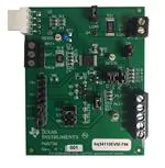
bq34110EVM-796 Evaluation Module
This evaluation module (EVM) is a complete evaluation system for the bq34110. This EVM includes one
bq34110 circuit module, an external current sense resistor. A separate orderable EV2400 PC interface
board for gas gauge along with a PC USB cable, and Microsoft® Windows® based PC software is needed
when using this EVM. The circuit module includes one bq34110 integrated circuit and all other onboard
components necessary to monitor and predict capacity for a system-side or removable battery pack fuel
gauge solution. With the EV2400 users can:
• Read the bq34110 data registers
• Program the chipset for different configurations
• Log cycling data for further evaluation
• Evaluate the overall functionality under different charge and discharge conditions
1
2
3
4
5
Contents
Features ....................................................................................................................... 2
1.1
Kit Contents.......................................................................................................... 2
1.2
Ordering Information ............................................................................................... 2
1.3
bq34110 Circuits Module Performance Specification Summary .............................................. 2
bq34110EVM Quick Start Guide ........................................................................................... 3
2.1
Items Required for EVM Setup and Evaluation ................................................................. 3
2.2
Battery Management Studio (bqStudio) Software .............................................................. 3
2.3
EV2400 Firmware Updater ........................................................................................ 3
2.4
Update bq34110 Device Firmware ............................................................................... 3
2.5
EVM Connections ................................................................................................... 3
2.6
PC Interface Connection ........................................................................................... 5
Operation ..................................................................................................................... 6
3.1
Starting the Program ............................................................................................... 6
3.2
Setting Programmable bq34110 Options ........................................................................ 7
3.3
Calibration ........................................................................................................... 9
3.4
Programming Screen ............................................................................................. 10
3.5
Advanced Comm I2C Screen .................................................................................... 11
3.6
Golden Image Screen ............................................................................................ 12
3.7
Setting the CEDV Parameters ................................................................................... 13
Circuit Module Physical Layout, Bill of Materials and Schematic .................................................... 14
4.1
Board Layout ....................................................................................................... 14
4.2
Bill of Materials .................................................................................................... 18
4.3
Schematic .......................................................................................................... 20
Related Documentation from Texas Instruments ...................................................................... 21
List of Figures
...................................................... 4
............................................................................................................ 6
Data Memory Screen........................................................................................................ 7
Calibration Screen ........................................................................................................... 9
Programming Screen ...................................................................................................... 10
Advanced Comm I2C Screen ............................................................................................. 11
Golden Image Window .................................................................................................... 12
1
bq34110 Circuit Module Connection to Pack and System Load
2
Registers Screen
3
4
5
6
7
SLUUBI1A – October 2016 – Revised July 2018
Submit Documentation Feedback
Copyright © 2016–2018, Texas Instruments Incorporated
bq34110EVM-796 Evaluation Module
1
�Features
www.ti.com
8
CEDV Coefficients Calculation Flow ..................................................................................... 13
9
Top Silk Screen............................................................................................................. 14
10
Top Assembly............................................................................................................... 15
11
Top Layer
12
13
...................................................................................................................
Bottom Layer................................................................................................................
bq34110EVM Schematic ..................................................................................................
16
17
20
List of Tables
........................................................................................................
1
Ordering Information
2
Performance Specification Summary ..................................................................................... 2
3
Cell Configuration Jumper Placement
4
EVM Pin Descriptions ....................................................................................................... 5
5
Circuit Module to EV2400 Connections ................................................................................... 5
6
Bill of Materials
....................................................................................
.............................................................................................................
2
4
18
(1) (2)
1 Features
This EVM has the following features:
• Complete evaluation system for the bq34110 CEDV gas gauge
• Populated circuit module for quick setup
• Personal computer (PC) software and interface board for easy evaluation
• Software allows data logging for system analysis
1.1
Kit Contents
The following items are included in the EVM kit:
• bq34110 circuit module
• Cable to connect the EVM to an EV2400 communications interface adapter
This EVM is used for the evaluation of the bq34110. Visit the product web folder (bq34110) to properly
configure the bq34110.
1.2
Ordering Information
Table 1 lists the EVM ordering information.
Table 1. Ordering Information
1.3
Part Number
EVM Part Number
Configuration
Chemistry
bq34110
bq34110EVM-796
3 V–48 V
Li-Ion, Li-Polymer, LiFePO4, PbA, NiMH, NiCd
bq34110 Circuits Module Performance Specification Summary
Table 2 summarizes the performance specifications of the bq34110 circuit module.
Table 2. Performance Specification Summary
Specification
(1)
(2)
2
Min
Typ
Max
Units
Input voltage BAT+ to BAT– in 1S mode
3
4
5
V
Input voltage BAT+ to BAT– in multicell
6
28
48
V
Charge and discharge current
0
2
7
A
Microsoft, Windows are registered trademarks of Microsoft Corporation.
All other trademarks are the property of their respective owners.
bq34110EVM-796 Evaluation Module
SLUUBI1A – October 2016 – Revised July 2018
Submit Documentation Feedback
Copyright © 2016–2018, Texas Instruments Incorporated
�bq34110EVM Quick Start Guide
www.ti.com
2
bq34110EVM Quick Start Guide
This section provides the step-by-step procedures required to take a new EVM and configure it for
operation in a laboratory environment.
2.1
Items Required for EVM Setup and Evaluation
The following items are required to set up and evaluate the EVM:
• bq34110 EVM
• EV2400 communications interface adapter
• USB cable to the communications interface adapter to the computer
• Windows 7 capable PC (or higher)
• DC power supply. (Constant current and constant voltage capability is desirable.)
If using the EV2300 (older version of interface adapter), USB drivers need to be installed. See the EV2300
product page for details: http://www.ti.com/tool/EV2300
2.2
Battery Management Studio (bqStudio) Software
bqStudio is a graphical user interface that allows the user to interact with the bq34110 device.
1. Download the latest version of bqStudio. The latest version listed as BQSTUDIOTEST is
recommended since it will contain the latest improvements (bq34110 needs v1.3.80 or later).
2. Run the installer. Make sure to ‘Run as Administrator’
3. Follow the on-screen instructions until completing the software installation.
4. Before starting the evaluation software, connect the EV2400 to the PC using the USB cable. The
EV2400 driver will install automatically.
2.3
EV2400 Firmware Updater
The EV2400 firmware is updated periodically. The bqStudio software will indicate which firmware version
is detected in the Dashboard. It is recommended to use v0.18 or later. If needed, the EV2400 Firmware
Updater is available at http://www.ti.com/tool/ev2400. The EV2400 User’s guide contains detailed
instructions for using the Firmware Updater.
2.4
Update bq34110 Device Firmware
The bq34110 may need updated firmware. Updating to the latest firmware version is recommended if it is
not already using the latest version.
1. 1. Download the latest bq34110 Firmware bundle from:
http://www.ti.com/product/BQ34110/toolssoftware
2. The installation will place the extracted files in a folder in ‘C:\ProgramData\Texas Instruments\’. Copy
the .bqz file to the directory: ‘C:\ti\BatteryManagementStudio\config’. This will ensure bqStudio has the
latest updates and tools for bq34110 evaluation.
3. Find the .srec file in the same folder from Step 2. Follow the directions in Section 3.5 to use bqStudio
to program the latest firmware .srec to the device.
4. Once programming is finished, the EVM is ready to use with the latest firmware.
2.5
EVM Connections
The bq34110 evaluation system comprises three hardware components: the bq34110 circuit module, the
EV2400 PC interface board, and the PC.
2.5.1
Connecting the bq34110 Circuit Module to a Battery Pack
Figure 1 illustrates the board connections to a battery pack.
SLUUBI1A – October 2016 – Revised July 2018
Submit Documentation Feedback
Copyright © 2016–2018, Texas Instruments Incorporated
bq34110EVM-796 Evaluation Module
3
�bq34110EVM Quick Start Guide
www.ti.com
EV2400
Computer
USB
I2C
+
Power
Supply
or Cells
Load
-
Figure 1. bq34110 Circuit Module Connection to Pack and System Load
2.5.2
Circuit Module Connections
Contacts on the circuit module provide the following connections:
• Direct connection to the battery pack (J7): BAT+ and BAT–
See Table 3 to configure J2 and J5 to support the voltage range for your pack.
Table 3. Cell Configuration Jumper Placement
Cell Configuration
Jumper Placement
J2:
Single cell or stack voltage less than 5 V
Place jumpers in the ≤ 5-V positions
Multicell:
Place jumpers in the > 5 V positions
J5:
•
4
Single cell:
Does not matter
Multicell:
Place the jumper to the appropriate setting for your series cell configuration
Attach BAT– to the bottom of the battery stack and attach BAT+ to the top of the battery stack.
Charger or load connection (J7): BAT+ and PACK–
Attach the load or power supply to the J7 terminal block. Connect the positive load or power supply
wire to the terminal block position labeled BAT+. Connect the ground wire for the load or power supply
to the terminal block position labeled PACK–.
bq34110EVM-796 Evaluation Module
SLUUBI1A – October 2016 – Revised July 2018
Submit Documentation Feedback
Copyright © 2016–2018, Texas Instruments Incorporated
�bq34110EVM Quick Start Guide
www.ti.com
•
•
•
•
2.5.3
I2C communication port (J1): I2C bus
Attach the communications interface adapter cable to J1 and to the I2C port on the EV2400.
Chip Enable (J4): CE
Place a jumper on CE enabling the REG25 regulator to power the bq34110.
External Learning Load: LOAD jumper and J8.
The external learning load can be configured using the on-board 20-Ω load resistor or an external
resistor attached to J8. The 20-Ω resistor can support a 2000-mAh single-cell configuration. Other
configurations require that a resistor be attached to J8. The LOAD jumper must be removed when
using the external load resistor.
ALERT1, ALERT2 (J6)
Place jumpers on J4 PU1 and PU2 to apply pull-up resistors to open drain outputs ALERT1 and
ALERT2. Monitor the outputs monitored on J6.
Pin Description
Table 4 lists the EVM pin descriptions.
Table 4. EVM Pin Descriptions
Pin Name
ALERT1
Open drain alert output
ALERT2
Open drain alert output
BAT+
Battery stack positive terminal
BAT–
Battery stack negative terminal
CE
Chip Enable
GND
Ground return
LEN
Optional LEN GPIO
PACK–
OPT EXT LOAD
2.6
Description
Pack negative terminal
Connection to apply an external learning load
SCL
I2C clock signal
SDA
I2C data signal
VEN
Optional VEN GPIO. When set, this pin is used to control the external voltage
divider for the BAT pin and disables the internal voltage divider.
PC Interface Connection
The following steps configure the hardware for interfacing with the PC:
1. Connect the bq34110 EVM to the EV2400 using wire leads as shown in Table 3.
2. Connect the PC USB cable to the EV2400 and the PC USB port.
Table 5. Circuit Module to EV2400 Connections
bq34110EVM
EV2300
EV2400
SDA
SDA
PORT2 - SDA
SCL
SCL
PORT2 - SCL
VSS
GND
PORT2 - VSS
The bq34110EVM-796 is now set up for operation.
SLUUBI1A – October 2016 – Revised July 2018
Submit Documentation Feedback
Copyright © 2016–2018, Texas Instruments Incorporated
bq34110EVM-796 Evaluation Module
5
�Operation
3
www.ti.com
Operation
This section provides instructions for operating the software.
3.1
Starting the Program
With the EV2400 and the bq34110EVM connected to the computer, run bqStudio from the Desktop or
installation directory. The initial window consists of a tools panel at the top and other child windows that
can be hidden, docked in various positions, or allowed to float as separate windows. When bqStudio first
starts up the DashBoard, the Registers, and Commands windows should be open. Additional windows can
be added by clicking the corresponding icons in the tools panel at the top of the main window.
The Scan (continuous scan) or Refresh (single time scan) buttons can be clicked in order to update the
data in the Registers and Data Memory windows.
bqStudio provides a logging function which logs selected Data Registers last received from the bq34110.
To enable this function, click the Start Log button. The default elapsed interval is 4000 milliseconds, to
change this interval, go to Windows, select Preferences, choose Registers, and change Scan/Log Interval
from 4000 to 1000 milliseconds. There is no need to log faster than 1 second as the gauge will not update
the registers faster than 1 second.
The Registers section contains parameters used to monitor gauging (see Figure 2). The Bit Registers
section provides a bit-level picture of status and fault registers. A green flag indicates that the bit is 0 (low
state) and a red flag indicates that the bit is 1 (high state). Data begins to appear once the Refresh
(single-time scan) button is selected, or it scans continuously if the Scan button is selected.
Figure 2. Registers Screen
6
bq34110EVM-796 Evaluation Module
SLUUBI1A – October 2016 – Revised July 2018
Submit Documentation Feedback
Copyright © 2016–2018, Texas Instruments Incorporated
�Operation
www.ti.com
3.2
Setting Programmable bq34110 Options
The bq34110 comes configured per the default settings detailed in the bq34110 Technical Reference
Manual (SLUUBF7). Ensure that the settings are correctly changed to match pack and applications for the
bq34110 solution being evaluated.
NOTE: The bq34110 comes up UNSEALED but not in FULL ACCESS. Execute the UNSEAL and
then the UNSEAL FULL ACCESS commands from the command window to enable access
to the data memory.
NOTE: The correct setting of these options is essential to get the best performance. The settings
can be configured using the Data Memory window (Figure 3).
Figure 3. Data Memory Screen
To read all the data from the bq34110 non-volatile flash memory, click on the Read All button on the Data
Memory window. Make sure the device is not sealed and in full access to read or write to the data
memory. To update a parameter, click on the desired parameter and a window will pop-up that provides
details on the selected parameter. Next, enter the value in the value textbox and press Enter. After Enter
has been pressed, bqStudio will update the selected parameter. The Import button in the Data Memory
window can be clicked in order to import an entire configuration from a specified *.gg.csv file.
The configuration can be saved to a file by clicking the Export button in the Data Memory window and
entering a file name. The configuration will be saved to a *.gg.csv file. The module calibration data is also
held in the bq34110 data memory. If the Gauge Dashboard is not displaying any information, then the
bq34110 may not be supported by the bqStudio version that is being used, a bqStudio upgrade may be
required.
SLUUBI1A – October 2016 – Revised July 2018
Submit Documentation Feedback
Copyright © 2016–2018, Texas Instruments Incorporated
bq34110EVM-796 Evaluation Module
7
�Operation
3.2.1
www.ti.com
Cell Configuration
The bq34110 operates in one of two modes for measuring battery voltage. Place jumpers on the J2 and
J5 headers to select the mode of operation. See the EVM Connections section.
For packs where the stack voltage is less than 5 V:
• Enable Calibration Mode on the device by pressing the CAL_TOGGLE button on the Commands
panel. Verify that the CAL_EN flag is set in the Manufacturing Status register.
• Update the Flash Update OK Voltage parameter on the Data Memory Configuration screen to
100mV (default is 2.8V). This parameter prevents flash updates when the measured voltage is below
this setting. This can later be updated to an appropriate voltage once the dividers are configured.
• Set the Number of Series Cells parameter to the appropriate value on the Data Memory
Configuration screen.
• Reset the gauge using the RESET button on the Commands panel.
• Calibrate the stack voltage. See the Calibration section.
NOTE: The EVM can support single cell applications, where the cell voltage can drop below 2.5 V,
by providing an external 3.3-V supply to power REGIN. For voltages below 2.5V, remove the
jumper from J2 – pins 3 and 4 (upper ≤ 5-V jumper location) and apply a 3.3-V supply to the
REGIN test point.
For packs where the stack voltage is greater than 5 V:
• Enable Calibration Mode on the device by pressing the CAL_TOGGLE button on the Commands
panel. Verify that the CAL_EN flag is set in the Manufacturing Status register.
• Update the Flash Update OK Voltage parameter on the Data Memory Configuration screen to
100mV (default is 2.8V). This parameter prevents flash updates when the measured voltage is below
this setting.
• Set the VEN_EN bit to “1” in the Pin Control Config in Data Memory on the Settings screen. This
enables the external voltage divider on the EVM and disables the internal voltage divider. The VEN pin
will pulse to enable the external resistor divider only during a voltage measurement to save power.
• Set the Number of Series Cells parameter to the appropriate value on the Data Memory
Configuration screen.
• Set the Voltage Divider parameter in Data Memory on the Calibration screen. This value should be
set based on the external resistor divider setting. (For example, use ~19,200 when the J5 header is set
to the 16V setting which divides the BAT+ voltage by 19.2).
• Reset the gauge using the RESET button on the Commands panel.
• Calibrate the stack voltage. See the Calibration section.
8
bq34110EVM-796 Evaluation Module
SLUUBI1A – October 2016 – Revised July 2018
Submit Documentation Feedback
Copyright © 2016–2018, Texas Instruments Incorporated
�Operation
www.ti.com
3.3
Calibration
The bq34110EVM must be calibrated to ensure accurate value reporting. This is done in the Calibration
window (Figure 4) in bqStudio.
Figure 4. Calibration Screen
3.3.1
Voltage Calibration
Voltage calibration instructions follow:
• Measure the voltage from BAT+ to BAT–, enter this value in the Applied Voltage field, and select the
Calibrate Voltage box.
• Press the Calibrate Gas Gauge button to calibrate the voltage measurement system.
• Deselect the Calibrate Voltage boxes after voltage calibration has completed.
3.3.2
Temperature Calibration
Temperature calibration instructions follow::
• Enter the room temperature in each of the Applied Temperature fields and select the Calibrate
Temperature box for the thermistor to be calibrated. The temperature values must be entered in
degrees Celsius.
• Press the Calibrate Gas Gauge button to calibrate the temperature measurement system.
• Deselect the Calibrate boxes after temperature calibration has completed.
SLUUBI1A – October 2016 – Revised July 2018
Submit Documentation Feedback
Copyright © 2016–2018, Texas Instruments Incorporated
bq34110EVM-796 Evaluation Module
9
�Operation
3.3.3
www.ti.com
Current Calibration
The gauge offers CC Offset and Board Offset calibration options to zero any residual current that may be
reported by the gauge. These calibrations are only required if the gauge does not report 0-mA current
when no current should be present.
• Select the CC Offset calibration option.
• Press the Calibrate Gas Gauge button to calibrate.
• Verify whether the current reports 0 mA. Proceed with the Board Offset Current calibration if current is
reported.
• Select the CC Offset calibration option.
• Press the Calibrate Gas Gauge button to calibrate.
• Verify whether the current reports 0 mA.
• Connect a 2-A load from BAT+ to PACK–.
• Enter –2000 in the Applied Current field and select the Calibrate Current box.
• Press the Calibrate Gas Gauge button to calibrate.
• Deselect the Calibrate Current box after current calibration has completed.
3.4
Programming Screen
Press the Programming button to select the Programming Update window (Figure 5). This window allows
the user to import the device firmware.
Figure 5. Programming Screen
3.4.1
Programming the Flash Memory
The Programming screen is used to initialize the device by loading the default .srec into the flash memory
(see Figure 5).
• Search for the .srec file using the Browse button.
• Press the Program button and wait for the download to complete.
• Press the Execute FW button after the programming has been completed.
– Press the Read Srec button to save the flash memory contents to the file. Wait for the download to
complete.
10
bq34110EVM-796 Evaluation Module
SLUUBI1A – October 2016 – Revised July 2018
Submit Documentation Feedback
Copyright © 2016–2018, Texas Instruments Incorporated
�Operation
www.ti.com
3.5
Advanced Comm I2C Screen
Press the Advanced Comm button to select the Advanced Comm I2C window. This tool provides access
to parameters using I2C and Manufacturing Access commands (see Figure 6).
Figure 6. Advanced Comm I2C Screen
Examples:
Reading an I2C Command:
• Read SBData Voltage (0x08)
– Start Register = 08, 2 bytes. Press the Read button.
– Word = 0x103B, which is hexadecimal for 4155 mV
Sending an EOS_EN to start gauging via ManufacturerAccessControl():
• Send EOS_EN() (0x0021) to ManufacturerAccessControl().
– Start Register = 0x3e. Data = 21 00. Press the Write button.
SLUUBI1A – October 2016 – Revised July 2018
Submit Documentation Feedback
Copyright © 2016–2018, Texas Instruments Incorporated
bq34110EVM-796 Evaluation Module
11
�Operation
3.6
www.ti.com
Golden Image Screen
Press the Golden Image button to select the Golden Image window. This window allows the user to
export the device firmware as an .srec, .bq.fs and .df.fs files.
Figure 7. Golden Image Window
3.6.1
Exporting the Flash Memory
The .srec file contains the full flash memory. The .bq.fs contains the program memory portion for the flash
memory and the .df.fs contains the data flash portion of the flash memory (seeFigure 7).
• Select the directory location to export the files.
• Enter the file name for the files.
• Select the files types to export.
• Press the Create Image File button to export the memory and create the files.
12
bq34110EVM-796 Evaluation Module
SLUUBI1A – October 2016 – Revised July 2018
Submit Documentation Feedback
Copyright © 2016–2018, Texas Instruments Incorporated
�Operation
www.ti.com
3.7
Setting the CEDV Parameters
To ease evaluation of the bq34110, users can obtain the CEDV parameters from our online gauging
parameter calculator (GPC) for the CEDV gauges tool (www.ti.com/tool/GPCCEDV). After programming
the design parameters to the gauge, the EVM can be used to obtain the experimental data needed to
calculate the CEDV coefficients.
Figure 8. CEDV Coefficients Calculation Flow
The equipment necessary is as follows:
• bqStudio software
• bq34110EVM-796
• Power supply able to source/sink current. A DC power supply and electronic load.
See the Simple Guide to CEDV Data Collection for Gauging Parameter Calculator (GPC) user's guide
(SLUUB45) for a detailed explanation of the CEDV coefficients data collection process and GPC tool
configuration.
Use the GPC Cycle plug-in to control the collection of the log files and the GPCPackager plug-in to
package the files into a zip file to import to the online GPCCHEM tool.
SLUUBI1A – October 2016 – Revised July 2018
Submit Documentation Feedback
Copyright © 2016–2018, Texas Instruments Incorporated
bq34110EVM-796 Evaluation Module
13
�Circuit Module Physical Layout, Bill of Materials and Schematic
4
www.ti.com
Circuit Module Physical Layout, Bill of Materials and Schematic
This section contains the board layout, bill of materials, and schematic for the bq34110 circuit module.
4.1
Board Layout
This section shows the printed circuit board (PCB) layers (Figure 9 through Figure 12) and assembly
drawing for the bq34110 module.
Figure 9. Top Silk Screen
14
bq34110EVM-796 Evaluation Module
SLUUBI1A – October 2016 – Revised July 2018
Submit Documentation Feedback
Copyright © 2016–2018, Texas Instruments Incorporated
�Circuit Module Physical Layout, Bill of Materials and Schematic
www.ti.com
Figure 10. Top Assembly
SLUUBI1A – October 2016 – Revised July 2018
Submit Documentation Feedback
Copyright © 2016–2018, Texas Instruments Incorporated
bq34110EVM-796 Evaluation Module
15
�Circuit Module Physical Layout, Bill of Materials and Schematic
www.ti.com
Figure 11. Top Layer
16
bq34110EVM-796 Evaluation Module
SLUUBI1A – October 2016 – Revised July 2018
Submit Documentation Feedback
Copyright © 2016–2018, Texas Instruments Incorporated
�Circuit Module Physical Layout, Bill of Materials and Schematic
www.ti.com
Figure 12. Bottom Layer
SLUUBI1A – October 2016 – Revised July 2018
Submit Documentation Feedback
Copyright © 2016–2018, Texas Instruments Incorporated
bq34110EVM-796 Evaluation Module
17
�Circuit Module Physical Layout, Bill of Materials and Schematic
4.2
www.ti.com
Bill of Materials
Table 6 lists the BOM for this EVM.
Table 6. Bill of Materials
Qty
18
Reference
Designator
Value
3300pF
Description
Size
Part Number
Manufacturer
CAP, CERM, 3300 pF, 50 V, +/- 10%, X7R, 0603
0603
GRM188R71H332KA01D
Murata
CAP, CERM, 0.1 µF, 50 V, +/- 10%, X7R, 0603
0603
GRM188R71H104KA93D
Murata
1
C1
4
C2, C3, C4, C5
1
C6
1uF
CAP, CERM, 1 µF, 50 V, +/- 10%, X7R, 0805
0805
GRM21BR71H105KA12L
Murata
1
D1
5.6V
Diode, Zener, 5.6 V, 300 mW, SOD-523
SOD-523
BZT52C5V6T-7
Diodes Inc.
1
H1
Cable
Used in PnP output
CBL002
Any
1
J1
Header (friction lock), 100mil, 4x1, R/A, TH
4x1 R/A Header
22-05-3041
Molex
1
J2
Header, 100mil, 8x1, Tin, TH
Header, 8x1, 100mil, TH
PEC08SAAN
Sullins Connector Solutions
3
J3, J8, J10
Header, 100mil, 2x1, Tin, TH
Header, 2 PIN, 100mil, Tin
PEC02SAAN
Sullins Connector Solutions
2
J4, J5
Header, 100mil, 3x2, Tin, TH
3x2 Header
PEC03DAAN
Sullins Connector Solutions
1
J6
Terminal Block, 3.5mm Pitch, 5x1, TH
17.5x8.2x6.5mm
ED555/5DS
On-Shore Technology
1
J7
Terminal Block, 3.5 mm, 3x1, Tin, TH
Terminal Block, 3.5 mm,
3x1, TH
39357-0003
Molex
1
J9
Terminal Block, 3.5 mm, 2x1, Tin, TH
Terminal Block, 3.5 mm,
2x1, TH
39357-0002
Molex
1
Q1
60V
MOSFET, N-CH, 60 V, 0.17 A, SOT-23
SOT-23
2N7002-7-F
Diodes Inc.
1
Q2
-50V
MOSFET, P-CH, -50 V, -0.13 A, SOT-323
SOT-323
BSS84W-7-F
Diodes Inc.
1
Q3
50V
MOSFET, N-CH, 50 V, 0.2 A, SOT-323
SOT-323
BSS138W-7-F
Diodes Inc.
1
Q4
30V
MOSFET, N-CH, 30 V, 5 A, SON 2x2mm
SON 2x2mm
CSD17313Q2
Texas Instruments
1
R1
10k
RES, 10k ohm, 5%, 0.1W, 0603
0603
CRCW060310K0JNEA
Vishay-Dale
3
R2, R10, R11
100k
RES, 100 k, 1%, 0.1 W, 0603
0603
CRCW0603100KFKEA
Vishay-Dale
2
R3, R4
10.0k
RES, 10.0 k, 1%, 0.1 W, 0603
0603
CRCW060310K0FKEA
Vishay-Dale
1
R5
165k
RES, 165 k, 1%, 0.1 W, 0603
0603
CRCW0603165KFKEA
Vishay-Dale
4
R6, R7, R16, R20
100
RES, 100, 1%, 0.1 W, 0603
0603
CRCW0603100RFKEA
Vishay-Dale
1
R8
16.5k
RES, 16.5 k, 0.1%, 0.1 W, 0603
0603
RG1608P-1652-B-T5
Susumu Co Ltd
3
R9, R12, R13
300k
RES, 300 k, 0.1%, 0.1 W, 0603
0603
RG1608P-304-B-T5
Susumu Co Ltd
4
R14, R15, R17, R19
1.0k
RES, 1.0k ohm, 5%, 0.1W, 0603
0603
CRCW06031K00JNEA
Vishay-Dale
1
R18
0.01
RES, 0.01, 1%, 1 W, 2010
2010
WSL2010R0100FEA18
Vishay-Dale
1
R21
20
RES, 20, 5%, 1 W, AEC-Q200 Grade 0, 2512
2512
CRCW251220R0JNEG
Vishay-Dale
1
R22
1.0Meg
RES, 1.0 M, 5%, 0.1 W, 0603
0603
CRCW06031M00JNEA
Vishay-Dale
1
RT1
10.0k ohm
Thermistor NTC, 10.0k ohm, 1%, Disc, 5x8.4 mm
Disc, 5x8.4 mm
103AT-2
SEMITEC Corporation
3
TP1, TP2, TP3
Test Point, Miniature, White, TH
White Miniature Testpoint
5002
Keystone
1
U1
Multi-Chemistry CEDV Gas Gauge for Rarely Discharged
Applications, PW0014A
PW0014A
BQ34110PWR
Texas Instruments
0.1uF
White
bq34110EVM-796 Evaluation Module
SLUUBI1A – October 2016 – Revised July 2018
Submit Documentation Feedback
Copyright © 2016–2018, Texas Instruments Incorporated
�Circuit Module Physical Layout, Bill of Materials and Schematic
www.ti.com
Table 6. Bill of Materials (continued)
Qty
2
Reference
Designator
Value
U2, U3
Description
Size
Part Number
Manufacturer
ESD in 0402 Package with 10 pF Capacitance and 6 V Breakdown, 1
Channel, -40 to +125 degC, 2-pin X2SON (DPY), Green (RoHS & no
Sb/Br)
DPY0002A
TPD1E10B06DPYR
Texas Instruments
SLUUBI1A – October 2016 – Revised July 2018
Submit Documentation Feedback
bq34110EVM-796 Evaluation Module
Copyright © 2016–2018, Texas Instruments Incorporated
19
�Circuit Module Physical Layout, Bill of Materials and Schematic
4.3
www.ti.com
Schematic
Figure 13 illustrates the schematic for the EVM.
Figure 13. bq34110EVM Schematic
20
bq34110EVM-796 Evaluation Module
SLUUBI1A – October 2016 – Revised July 2018
Submit Documentation Feedback
Copyright © 2016–2018, Texas Instruments Incorporated
�Related Documentation from Texas Instruments
www.ti.com
5
Related Documentation from Texas Instruments
bq34110 data sheet, bq34110 Multi-Chemistry CEDV Battery Gas Gauge for Rarely Discharged
Applications datasheet, SLUSCI1B
bq34110 Technical Reference Manual, SLUUBF7
SLUUBI1A – October 2016 – Revised July 2018
Submit Documentation Feedback
Copyright © 2016–2018, Texas Instruments Incorporated
bq34110EVM-796 Evaluation Module
21
�Revision History
www.ti.com
Revision History
NOTE: Page numbers for previous revisions may differ from page numbers in the current version.
Changes from October 25, 2016 to July 25, 2018 ........................................................................................................... Page
•
•
•
•
•
•
•
•
•
•
•
22
Removed references throughout the document for EV2300 which is being discontinued for new designs. ................. 1
Updated image and example to show the transaction log. .......................................................................... 1
Added additional jumper settings descriptions within the schematic image. ...................................................... 2
Changed Quick Start Guide to include steps to set up EV2400 firmware and bq34110 firmware.............................. 3
Added Additional description for VEN pin functionality. .............................................................................. 5
Clarified the instructions for putting the device in UNSEAL FULL ACCESS mode. .............................................. 7
Updated Cell Configuration section to include additional important steps. ........................................................ 8
Updated image and example to show the transaction log. ......................................................................... 11
Corrected device name. ................................................................................................................ 13
Added additional jumper settings descriptions within the schematic image. ..................................................... 20
Updated with links to relevant documents for the bq34110. ....................................................................... 21
Revision History
SLUUBI1A – October 2016 – Revised July 2018
Submit Documentation Feedback
Copyright © 2016–2018, Texas Instruments Incorporated
�IMPORTANT NOTICE FOR TI DESIGN INFORMATION AND RESOURCES
Texas Instruments Incorporated (‘TI”) technical, application or other design advice, services or information, including, but not limited to,
reference designs and materials relating to evaluation modules, (collectively, “TI Resources”) are intended to assist designers who are
developing applications that incorporate TI products; by downloading, accessing or using any particular TI Resource in any way, you
(individually or, if you are acting on behalf of a company, your company) agree to use it solely for this purpose and subject to the terms of
this Notice.
TI’s provision of TI Resources does not expand or otherwise alter TI’s applicable published warranties or warranty disclaimers for TI
products, and no additional obligations or liabilities arise from TI providing such TI Resources. TI reserves the right to make corrections,
enhancements, improvements and other changes to its TI Resources.
You understand and agree that you remain responsible for using your independent analysis, evaluation and judgment in designing your
applications and that you have full and exclusive responsibility to assure the safety of your applications and compliance of your applications
(and of all TI products used in or for your applications) with all applicable regulations, laws and other applicable requirements. You
represent that, with respect to your applications, you have all the necessary expertise to create and implement safeguards that (1)
anticipate dangerous consequences of failures, (2) monitor failures and their consequences, and (3) lessen the likelihood of failures that
might cause harm and take appropriate actions. You agree that prior to using or distributing any applications that include TI products, you
will thoroughly test such applications and the functionality of such TI products as used in such applications. TI has not conducted any
testing other than that specifically described in the published documentation for a particular TI Resource.
You are authorized to use, copy and modify any individual TI Resource only in connection with the development of applications that include
the TI product(s) identified in such TI Resource. NO OTHER LICENSE, EXPRESS OR IMPLIED, BY ESTOPPEL OR OTHERWISE TO
ANY OTHER TI INTELLECTUAL PROPERTY RIGHT, AND NO LICENSE TO ANY TECHNOLOGY OR INTELLECTUAL PROPERTY
RIGHT OF TI OR ANY THIRD PARTY IS GRANTED HEREIN, including but not limited to any patent right, copyright, mask work right, or
other intellectual property right relating to any combination, machine, or process in which TI products or services are used. Information
regarding or referencing third-party products or services does not constitute a license to use such products or services, or a warranty or
endorsement thereof. Use of TI Resources may require a license from a third party under the patents or other intellectual property of the
third party, or a license from TI under the patents or other intellectual property of TI.
TI RESOURCES ARE PROVIDED “AS IS” AND WITH ALL FAULTS. TI DISCLAIMS ALL OTHER WARRANTIES OR
REPRESENTATIONS, EXPRESS OR IMPLIED, REGARDING TI RESOURCES OR USE THEREOF, INCLUDING BUT NOT LIMITED TO
ACCURACY OR COMPLETENESS, TITLE, ANY EPIDEMIC FAILURE WARRANTY AND ANY IMPLIED WARRANTIES OF
MERCHANTABILITY, FITNESS FOR A PARTICULAR PURPOSE, AND NON-INFRINGEMENT OF ANY THIRD PARTY INTELLECTUAL
PROPERTY RIGHTS.
TI SHALL NOT BE LIABLE FOR AND SHALL NOT DEFEND OR INDEMNIFY YOU AGAINST ANY CLAIM, INCLUDING BUT NOT
LIMITED TO ANY INFRINGEMENT CLAIM THAT RELATES TO OR IS BASED ON ANY COMBINATION OF PRODUCTS EVEN IF
DESCRIBED IN TI RESOURCES OR OTHERWISE. IN NO EVENT SHALL TI BE LIABLE FOR ANY ACTUAL, DIRECT, SPECIAL,
COLLATERAL, INDIRECT, PUNITIVE, INCIDENTAL, CONSEQUENTIAL OR EXEMPLARY DAMAGES IN CONNECTION WITH OR
ARISING OUT OF TI RESOURCES OR USE THEREOF, AND REGARDLESS OF WHETHER TI HAS BEEN ADVISED OF THE
POSSIBILITY OF SUCH DAMAGES.
You agree to fully indemnify TI and its representatives against any damages, costs, losses, and/or liabilities arising out of your noncompliance with the terms and provisions of this Notice.
This Notice applies to TI Resources. Additional terms apply to the use and purchase of certain types of materials, TI products and services.
These include; without limitation, TI’s standard terms for semiconductor products http://www.ti.com/sc/docs/stdterms.htm), evaluation
modules, and samples (http://www.ti.com/sc/docs/sampterms.htm).
Mailing Address: Texas Instruments, Post Office Box 655303, Dallas, Texas 75265
Copyright © 2018, Texas Instruments Incorporated
�


 工商网监
湘ICP备2023018690号
工商网监
湘ICP备2023018690号
