BQ40Z80
BQ40Z80
SLUSBV4B – JUNE 2018 – REVISED SEPTEMBER
2020
SLUSBV4B – JUNE 2018 – REVISED SEPTEMBER 2020
www.ti.com
BQ40Z80 2-Series to 6-Series Li-Ion Battery Pack Manager
authentication for 2-series up to 6-series cell li-ion and
li-polymer battery packs.
2 Applications
•
•
•
•
1k
PACK+
10k
100
DSG
BAT
LEDCNTLA/
PDSG/GPIO
VC6
LEDCNTLB/GPIO
VC5
LEDCNTLC/GPIO
DISP*/TS4/
ADCIN2/GPIO
/DISP*/GPIO
VC4
VC3
SMBC
SMBC
VC2
SMBD
SMBD
VC1
PDSG/GPIO
TS3/ADCIN1/
GPIO
Industrial Appliances and Robots
Handheld Garden and Power Tools
Battery Powered Vacuums
Energy Storage Systems and UPS
4.00 mm × 4.00 mm
PACK
•
•
•
•
BODY SIZE (NOM)
VQFN (32)
TS2
•
PACKAGE
BQ40Z80
TS1
•
Device Information
PART NUMBER
SRN
•
VCC
•
The BQ40Z80 device supports TURBO Mode 2.0/Intel
Dynamic Battery Power Technology (DBPTv2) by
providing the available max power and max current to
the host system. The device has eight multifunction
pins that can be configured as thermal inputs, ADC
inputs, general purpose input/output (GPIO) pins, a
presence pin, LED functions, display button input, or
other functions. Status and flag registers are
mappable to the GPIOs and used as interrupts to the
host processor.
PCHG
•
•
•
Elliptic Curve Cryptography (ECC) or SHA-1
authentication with secure memory for authentication
keys enables identification of genuine battery packs.
PBI
•
SRP
•
Using its integrated high-performance analog
peripherals, the BQ40Z80 device measures and
maintains an accurate record of available capacity,
voltage, current, temperature, and other critical
parameters in li-ion or li-polymer batteries, and reports
this information to the system host controller over an
SMBus v1.1 compatible interface.
CHG
•
Fully integrated 2-series to 6-series li-ion or lipolymer cell battery pack manager and protection
Next-generation patented Impedance Track®
Technology accurately measures available charge
in li-ion and li-polymer batteries
Configurable multifunction pins to support a variety
of applications
Supports either Elliptic Curve Cryptography (ECC)
or SHA-1 authentication
High-side N-CH protection FET drive
Integrated cell balancing while charging or at rest
Supports 29-Ah batteries natively, and larger
capacities with scaling
Full array of programmable protection features
– Voltage
– Current
– Temperature
– Charge timeout
– CHG/DSG FETs
– AFE
Sophisticated charge algorithms
– JEITA
– Enhanced charging
– Adaptive charging
– Cell balancing
Supports TURBO Mode 2.0/Intel® Dynamic Battery
Power Technology (DBPTv2)
Diagnostic Lifetime Data Monitor and Black Box
Recorder
LED display
Supports two-wire SMBus v1.1 interface
IATA support
Compact package: 32-lead QFN (RSM)
FUSE
•
VSS
1 Features
PRES*/SHUTDN*/
DISP*/PDSG/GPIO
PRES*
PACK-
Simplified Schematic
3 Description
The BQ40Z80 device, incorporating patented
Impedance Track™ technology, is a fully integrated,
single-chip, pack-based solution that provides a rich
array of features for gas gauging, protection, and
An IMPORTANT NOTICE at the end of this data sheet addresses availability, warranty, changes, use in safety-critical applications,
Submit Document Feedback
Copyright
© 2020 Texas
Instruments
Incorporated
intellectual
property
matters
and other important disclaimers. PRODUCTION DATA.
Product Folder Links: BQ40Z80
1
�BQ40Z80
www.ti.com
SLUSBV4B – JUNE 2018 – REVISED SEPTEMBER 2020
Table of Contents
1 Features............................................................................1
2 Applications..................................................................... 1
3 Description.......................................................................1
4 Revision History.............................................................. 2
5 Description (continued).................................................. 3
6 Pin Configuration and Functions...................................3
Pin Functions.................................................................... 3
7 Specifications.................................................................. 8
7.1 Absolute Maximum Ratings........................................ 8
7.2 ESD Ratings............................................................... 8
7.3 Recommended Operating Conditions.........................8
7.4 Thermal Information....................................................9
7.5 Electrical Characteristics.............................................9
7.6 Typical Characteristics.............................................. 17
8 Detailed Description......................................................20
8.1 Overview................................................................... 20
8.2 Functional Block Diagram......................................... 20
8.3 Feature Description...................................................21
8.4 Device Functional Modes..........................................25
9 Applications and Implementation................................ 26
9.1 Application Information............................................. 26
9.2 Typical Applications.................................................. 26
10 Power Supply Recommendations..............................31
11 Layout........................................................................... 32
11.1 Layout Guidelines................................................... 32
11.2 Layout Examples.....................................................34
12 Device and Documentation Support..........................37
12.1 Documentation Support.......................................... 37
12.2 Receiving Notification of Documentation Updates..37
12.3 Support Resources................................................. 37
12.4 Trademarks............................................................. 37
12.5 Electrostatic Discharge Caution..............................37
12.6 Glossary..................................................................37
13 Mechanical, Packaging, and Orderable
Information.................................................................... 37
4 Revision History
NOTE: Page numbers for previous revisions may differ from page numbers in the current version.
Changes from Revision A (June 2018) to Revision B (September 2020)
Page
• Deleted the 7-series device option in the data sheet..........................................................................................1
• Deleted VC7 I/O details...................................................................................................................................... 3
• Changed high-voltage GPIO default from 7-series cell option to GPIO..............................................................9
• Deleted 7-series cell option and BQ40Z80 multifunction pin combinations......................................................22
• Changed the 7-series EVM schematic for the 6-series EVM schematic.......................................................... 26
• Updated the layout examples........................................................................................................................... 34
2
Submit Document Feedback
Copyright © 2020 Texas Instruments Incorporated
Product Folder Links: BQ40Z80
�BQ40Z80
www.ti.com
SLUSBV4B – JUNE 2018 – REVISED SEPTEMBER 2020
5 Description (continued)
The BQ40Z80 device provides software-based 1st- and 2nd-level safety protection against overvoltage,
undervoltage, overcurrent, short-circuit current, overload, and overtemperature conditions, as well as other packand cell-related faults. The compact 32-lead QFN package minimizes solution cost and size for smart batteries,
while providing maximum functionality and safety for battery gauging applications.
VC6
PBI
BAT
CHG
PCHG
NC
DSG
PACK
32
31
30
29
28
27
26
25
6 Pin Configuration and Functions
SMBC
NC
7
18
SMBD
SRP
8
17
/PRES//SHUTDOWN//DISP/PDSG/GPIO
16
19
PDSG/GPIO
6
15
LEDCNTLA/PDSG/GPIO
SRN
/DISP/GPIO
20
14
5
NC
LEDCNTLB/GPIO
VC1
13
21
/DISP/TS4/ADCIN2/GPIO
4
12
LEDCNTLC/GPIO
VC2
TS3/ADCIN1/GPIO
22
11
3
TS2
FUSE
VC3
9
VCC
23
10
24
2
TS1
1
VC4
VSS
VC5
Not to Scale
Figure 6-1. RSM Package 32-Pin VQFN with Exposed Thermal Pad Top View
Pin Functions
PIN
NAME
VC5
VC4
VC3
VC2
NUMBER
TYPE
1
2
3
4
AI(1)
DESCRIPTION
Sense voltage input pin for the fifth cell from the bottom of the stack, balance current
input for the fifth cell from the bottom of the stack, and return balance current for the
sixth cell from the bottom of the stack. Should be connected to the positive terminal of
the fifth cell from the bottom of stack with a 100-Ω series resistor and a 0.1-µF
capacitor to VC4. If not used, connect to VC4.
AI
Sense voltage input pin for the fourth cell from the bottom of the stack, balance
current input for the fourth cell from the bottom of the stack, and return balance
current for the fifth cell from the bottom of the stack. Should be connected to the
positive terminal of the fourth cell from the bottom of stack with a 100-Ω series
resistor and a 0.1-µF capacitor to VC3. If not used, connect to VC3.
AI
Sense voltage input pin for the third cell from the bottom of the stack, balance current
input for the third cell from the bottom of the stack, and return balance current for the
fourth cell from the bottom of the stack. Should be connected to the positive terminal
of the third cell from the bottom of stack with a 100-Ω series resistor and a 0.1-µF
capacitor to VC2. If not used, connect to VC2.
AI
Sense voltage input pin for the second cell from the bottom of the stack, balance
current input for the second cell from the bottom of the stack, and return balance
current for the third cell from the bottom of the stack. Should be connected to the
positive terminal of the second cell from the bottom of stack with a 100-Ω series
resistor and a 0.1-µF capacitor to VC1. If not used, connect to VC1.
Sense voltage input pin for the first cell from the bottom of the stack, balance current
input for the first cell from the bottom of the stack, and return balance current for the
second cell from the bottom of the stack. Should be connected to the positive terminal
of the first cell from the bottom of stack with a 100-Ω series resistor and a 0.1-µF
capacitor to VSS.
VC1
5
AI
SRN
6
I
NC
7
—
Analog input pin connected to the internal coulomb counter peripheral for integrating
a small voltage between SRP and SRN, where SRP is the top of the sense resistor
and charging current flows from SRP to SRN. Should be connected through an RC
filter to the sense resistor terminal connected to PACK– (not CELL–).
Not internally connected
Submit Document Feedback
Copyright © 2020 Texas Instruments Incorporated
Product Folder Links: BQ40Z80
3
�BQ40Z80
www.ti.com
SLUSBV4B – JUNE 2018 – REVISED SEPTEMBER 2020
PIN
NAME
TYPE
DESCRIPTION
SRP
8
I
Analog input pin connected to the internal coulomb counter peripheral for integrating
a small voltage between SRP and SRN, where SRP is the top of the sense resistor
and charging current flows from SRP to SRN. Should be connected through an RC
filter to the sense resistor positive terminal, which is connected to the least-positive
cells negative terminal.
VSS
9
P
Device ground
TS1
10
AI
Temperature sensor 1 thermistor input pin. Connect to thermistor-1. If not used,
connect directly to VSS and configure data flash accordingly.
TS2
11
AI
Temperature sensor 2 thermistor input pin. Connect to thermistor-2. If not used,
connect directly to VSS and configure data flash accordingly.
IO
Multifunction pin for TS3, ADCIN1, and GPIO. Can be configured in the control
registers. If not used, connect directly to VSS and configure data flash accordingly.
TS3: Temperature sensor 3 thermistor input pin. Connect to thermistor-3.
ADCIN1: General-purpose ADCIN pin. Connect properly scaled input to this pin.
GPIO: Customizable GPIO
TS3/ADCIN1/
GPIO
12
DISP/TS4/ADCIN2/GPIO
13
IO
Multifunction pin for the display button, temperature sensor input, ADC input, or
GPIO. Can be configured in the control registers. If not used, connect directly to VSS
and configure data flash accordingly.
DISP: Connect to the display button or LED.
TS4: Temperature sensor 4 thermistor input pin. Connect to thermistor-4.
ADCIN2: General-purpose ADCIN pin. Connect properly scaled input to this pin.
GPIO: Customizable GPIO
NC
14
—
Not internally connected
DISP/GPIO
PDSG/GPIO
15
16
I/OD
Multifunction pin for the display button, or GPIO. Can be configured in the control
registers. If not used, connect directly to VSS and configure data flash accordingly.
DISP: Connect to the display button or LED.
GPIO: Customizable GPIO
I/OD
Multifunction pin for pre-discharge FET control, or GPIO. Can be configured in the
control registers. If not used, connect directly to VSS and configure data flash
accordingly.
PDSG: Connect to the N-CH FET to control PRE-DISCHARGE mode.
GPIO: Customizable GPIO
PRES/ SHUTDN/ DISP/
PDSG/GPIO
17
I/OD
Multifunction pin for host system present input, emergency system shutdown, LED
button control, pre-discharge control, or GPIO. Can be configured in the control
registers. If not used, connect directly to VSS and configure data flash accordingly.
PRES: Connect to host to detect system present input for a removable battery pack.
Do not pullup this pin.
SHUTDN: Emergency shutdown input for an embedded battery pack
DISP: Connect to the display button or LED.
PDSG: Connect to the N-CH FET to control PRE-DISCHARGE mode.
GPIO: Customizable GPIO
SMBD
18
I/OD
SMBus data pin
SMBC
19
I/OD
SMBus clock pin
LEDCNTLA/PDSG/GPIO
LEDCNTLB/GPIO
LEDCNTLC/GPIO
4
NUMBER
20
21
22
O
Multifunction pin for LED display, pre-discharge, or GPIO. If not used, connect to VSS
with a 20-kΩ resistor.
LEDCNTLA: LED display segment that drives the external LEDs, depending on the
firmware configuration.
PDSG: Connect to the N-CH FET to control PRE-DISCHARGE mode.
GPIO: Customizable GPIO
O
Multifunction pin for LED display or GPIO. If not used, connect to VSS with a 20-kΩ
resistor.
LEDCNTLB: LED display segment that drives the external LEDs, depending on the
firmware configuration.
GPIO: Customizable GPIO
O
Multifunction pin for LED display or GPIO. If not used, connect to VSS with a 20-kΩ
resistor.
LEDCNTLC: LED display segment that drives the external LEDs, depending on the
firmware configuration
GPIO: Customizable GPIO
Submit Document Feedback
Copyright © 2020 Texas Instruments Incorporated
Product Folder Links: BQ40Z80
�BQ40Z80
www.ti.com
SLUSBV4B – JUNE 2018 – REVISED SEPTEMBER 2020
PIN
NAME
NUMBER
TYPE
DESCRIPTION
FUSE
23
O
Fuse drive output pin. Can be OR'ed together into the fuse N-CH FET gate drive with
secondary protector. If not used, connect directly to VSS.
VCC
24
P
Secondary power supply input. Connect to the middle of protection FETs through the
series resistor.
PACK
25
AI
Pack sense input pin. Connect through the series resistor to PACK+.
DSG
26
O
NMOS discharge FET drive output pin. Connect to the DSG FET gate.
NC
27
—
Not internally connected.
PCHG
28
O
PMOS precharge FET drive output pin. Connect to the PCHG FET gate if the
precharge function is used. Leave floating if not used.
CHG
29
O
NMOS charge FET drive output pin. Connect to the CHG FET gate.
BAT
30
P
Primary power supply input pin. Connect through the diode and series resistor to the
top of the cell stack.
PBI
31
P
Power supply backup input pin. Connect to the 2.2-µF capacitor to VSS.
AI
Sense voltage input pin for the sixth cell from the bottom of the stack, balance current
input for the sixth cell from the bottom of the stack. Should be connected to the
positive terminal of the sixth cell from the bottom of stack with 100-Ω series resistor
and a 0.1-µF capacitor to VC5. If not used, connect to VC5.
VC6
(1)
32
P = Power Connection, O = Digital Output, AI = Analog Input, I = Digital Input, I/OD = Digital Input/Output
Submit Document Feedback
Copyright © 2020 Texas Instruments Incorporated
Product Folder Links: BQ40Z80
5
�BQ40Z80
www.ti.com
SLUSBV4B – JUNE 2018 – REVISED SEPTEMBER 2020
VC4
BAT
CDEN4
PACK
VCC
VC3
3.1 V
+
±
BATDET
CDEN3
PACK
Detector
ENVCC
VC2
PACKDET
PBI
Reference
System
Shutdown
Latch
1. 8 V
Domain
VC1
BAT
Control
Power Supply Control
ADC
CDEN2
SHOUT
ENBAT
ADC Mux
SHUTDOWN
CDEN1
Cell Balancing
VCC
CHGEN
BAT
CHG
Pump
2k
CHG
8k
2k
PCHG
CHGOFF
PCHGEN
Precharge
Drive
PACK
DSGEN
BAT
DSG
Pump
2k
DSG
DSGOFF
CHG, DSG Drive
Figure 6-2. Pin Equivalent Diagram 1
6
Submit Document Feedback
Copyright © 2020 Texas Instruments Incorporated
Product Folder Links: BQ40Z80
�BQ40Z80
www.ti.com
SLUSBV4B – JUNE 2018 – REVISED SEPTEMBER 2020
1.8 V
ADTHx
BAT
FUSEWKPUP
18 kΩ
2 kΩ
ADC Mux
TS1,2,3,4
ADC
FUSEEN
150 nA
2 kΩ
FUSE
1.8 V
1.8 V
100 kΩ
FUSEDIG
RCWKPUP
RCPUP
FUSE Drive
1 kΩ
RCIN
RCOUT
SMBCIN
100 kΩ
SMBC
Thermistor Inputs
SMBCOUT
SMBCEN
1 MΩ
PBI
100 kΩ
SMBDIN
RHOEN
SMBDOUT
10 kΩ
PRES
SMBD
SMBDEN
1 MΩ
SMBus Interface
RHOUT
100 kΩ
RHIN
High-Voltage GPIO
BAT
RLOEN
LED1, 2, 3
22.5 mA
RLOUT
100 kΩ
RLIN
LED Drive
Figure 6-3. Pin Equivalent Diagram 2
Submit Document Feedback
Copyright © 2020 Texas Instruments Incorporated
Product Folder Links: BQ40Z80
7
�BQ40Z80
www.ti.com
SLUSBV4B – JUNE 2018 – REVISED SEPTEMBER 2020
7 Specifications
7.1 Absolute Maximum Ratings
Over-operating free-air temperature range (unless otherwise noted)(1)
Supply voltage range,
VCC
MIN
MAX
BAT(2), VCC(2), PBI(2), PACK(2)
–0.3
35
V
SMBC, SMBD, DISP/GPIO, PDSG/GPIO, PRES/ SHUTDN/ DISP/
PDSG/GPIO(2)
–0.3
35
V
TS1, TS2, TS3/ADCIN1/GPIO, DISP/TS4/ADCIN2/GPIO
–0.3
VREG + 0.3
V
LEDCNTLA/PDSG/GPIO, LEDCNTLB/GPIO, LEDCNTLC/GPIO(2)
–0.3
VBAT + 0.3
V
SRP, SRN
Input voltage range, VIN
Output voltage range,
VO
UNIT
–0.3
VREG + 0.3
V
VC6
VC5 – 0.3
VSS + 35
V
VC5
VC4 – 0.3
VSS + 35
V
VC4
VC3 – 0.3
VSS + 35
V
VC3
VC2 – 0.3
VSS + 35
V
VC2
VC1 – 0.3
VSS + 35
V
VC1
V
VSS – 0.3
VSS + 35
CHG, DSG(2)
–0.3
43
PCHG, FUSE
–0.3
Maximum VSS current, ISS
35
V
50
mA
Functional temperature TFUNC
–40
110
Storage temperature, TSTG
–65
150
°C
300
°C
Lead temperature (soldering, 10 s), TSOLDER
(1)
(2)
Stresses beyond those listed under absolute maximum ratings may cause permanent damage to the device. These are stress ratings
only, and functional operation of the device at these or any other conditions beyond those indicated under recommended operating
conditions is not implied. Exposure to absolute–maximum–rated conditions for extended periods may affect device reliability.
A series 50-Ω or larger resistor is needed when voltage is applied beyond 28 V.
7.2 ESD Ratings
VALUE
V(ESD)
(1)
(2)
Electrostatic
discharge
Human-body model (HBM), per ANSI/ESDA/JEDEC JS-001(1)
±2000
Charged-device model (CDM), per JEDEC specification JESD22-C101(2)
±500
UNIT
V
JEDEC document JEP155 states that 500-V HBM allows safe manufacturing with a standard ESD control process.
JEDEC document JEP157 states that 250-V CDM allows safe manufacturing with a standard ESD control process.
7.3 Recommended Operating Conditions
Typical values stated where TA = 25°C and VCC = 25.2 V, Min/Max values stated where TA = –40°C to 85°C and
VCC = 2.2 V to 32 V (unless otherwise noted)
MIN
VCC
Supply voltage
BAT(1), VCC(1), PBI(1), PACK(1)
2.2
VSHUTDOWN–
Shutdown voltage
VPACK < VSHUTDOWN –
1.8
VSHUTDOWN+
Start-up voltage
VPACK > VSHUTDOWN– + VHYS
2.05
VHYS
Shutdown voltage
hysteresis
VSHUTDOWN+ – VSHUTDOWN–
VIN
8
Input voltage range
NOM
MAX
V
2.0
2.2
V
2.25
2.45
V
250
mV
SMBC, SMBD, DISP/GPIO, PDSG/GPIO, PRES/
SHUTDN/, DISP/PDSG/GPIO(1)
32
TS1, TS2, TS3/ADCIN1/GPIO, DISP/TS4/ADCIN2/GPIO
VREG
LEDCNTLA/PDSG/GPIO, LEDCNTLB/GPIO, LEDCNTLC/
GPIO(1)
VBAT
Submit Document Feedback
UNIT
32
V
Copyright © 2020 Texas Instruments Incorporated
Product Folder Links: BQ40Z80
�BQ40Z80
www.ti.com
SLUSBV4B – JUNE 2018 – REVISED SEPTEMBER 2020
Typical values stated where TA = 25°C and VCC = 25.2 V, Min/Max values stated where TA = –40°C to 85°C and
VCC = 2.2 V to 32 V (unless otherwise noted)
MIN
SRP, SRN
MAX
0.2
VC6
VVC5
VC5 + 5
VC5
VVC4
VC4 + 5
VC4
VVC3
VC3 + 5
VC3
VVC2
VC2 + 5
VC2
VVC1
VC1 + 5
VC1
VVSS
VSS + 5
VO
Output voltage
range
CPBI
External PBI
capacitor
2.2
TOPR
Operating
temperature
–40
(1)
NOM
–0.2
PCHG, FUSE(1)
32
UNIT
V
µF
85
°C
A series 50-Ω or larger resistor is needed when voltage is applied beyond 28 V.
7.4 Thermal Information
BQ40Z80
THERMAL
METRIC(1)
RSM (QFN)
UNIT
32 PINS
RθJA, High K
Junction-to-ambient thermal resistance
47.4
°C/W
RθJC(top)
Junction-to-case(top) thermal resistance
40.3
°C/W
RθJB
Junction-to-board thermal resistance
14.7
°C/W
ψJT
Junction-to-top characterization parameter
0.8
°C/W
ψJB
Junction-to-board characterization parameter
14.4
°C/W
RθJC(bottom)
Junction-to-case(bottom) thermal resistance
3.8
°C/W
(1)
For more information about traditional and new thermal metrics, see the Semiconductor and IC Package Thermal Metrics application
report, SPRA953.
7.5 Electrical Characteristics
Typical values stated where TA = 25°C and VCC = 21.6 V, Min/Max values stated where TA = –40°C to 85°C and
VCC = 2.2 V to 32 V unless otherwise noted
PARAMETER
CONDITIONS
MIN
TYP
MAX
UNIT
Supply Currents
INORMAL
ISLEEP
NORMAL mode
SLEEP mode
CPU not active, CHG on. DSG on, High Frequency
Oscillator on, Low Frequency Oscillator on, REG18
on, ADC on, ADC_Filter on, CC_Filter on, CC on,
LED/Buttons/GPIOs off, SMBus not active, no Flash
write
663
µA
CPU not active, CHG on, DSG on, High Frequency
Oscillator off, Low Frequency Oscillator on, REG18
on, ADC off, ADC_Filter off, CC_Filter off, LED/
Buttons/GPIOs off, SMBus not active, no Flash
write
96
µA
CPU not active, CHG off. DSG on, High Frequency
Oscillator off, Low Frequency Oscillator on, REG18
on, ADC off, ADC_Filter off, CC_Filter off, LED/
Buttons/GPIOs off, SMBus not active, no Flash
write, BAT = 14.4 V
90
µA
Submit Document Feedback
Copyright © 2020 Texas Instruments Incorporated
Product Folder Links: BQ40Z80
9
�BQ40Z80
www.ti.com
SLUSBV4B – JUNE 2018 – REVISED SEPTEMBER 2020
Typical values stated where TA = 25°C and VCC = 21.6 V, Min/Max values stated where TA = –40°C to 85°C and
VCC = 2.2 V to 32 V unless otherwise noted
PARAMETER
ISHUTDOWN
SHUTDOWN mode
CONDITIONS
MIN
CPU not active, CHG off. DSG off, High Frequency
Oscillator off, Low Frequency Oscillator off, REG18
off, ADC off, ADC_Filter off, CC_Filter off, LED/
Buttons/GPIOs off, SMBus not active, no Flash
write, BAT = 14.4 V
TYP
MAX
1.4
UNIT
µA
Power Supply Control
VSWITCHOVER–
BAT to VCC switchover
voltage
VBAT < VSWITCHOVER–
VSWITCHOVER+
VCC to BAT switchover
voltage
VBAT > VSWITCHOVER– + VHYS
VHYS
Switchover voltage
hysteresis
VSWITCHOVER+ – VSWITCHOVER–
ILKG
Input Leakage Current
Internal pulldown
resistance
RPD
1.95
2.1
2.2
V
2.9
3.1
3.25
V
1000
mV
BAT pin, BAT = 0 V, VCC = 32 V, PACK = 32 V
1
PACK pin, BAT = 32 V, VCC = 0 V, PACK = 0 V
1
BAT and PACK terminals, BAT = 0 V, VCC = 0 V,
PACK = 0 V, PBI = 32 V
1
PACK
µA
30
40
50
kΩ
1.51
1.55
1.59
V
70
100
130
mV
200
300
400
µs
AFE Power-On Reset
VREGIT–
Negative-going voltage
input
VREG
VHYS
Power-on reset hysteresis
VREGIT+ – VREGIT–
tRST
Power-on reset time
AFE Watchdog Reset and Wake Timer
tWDT
AFE watchdog timeout
tWAKE
AFE wake timer
tFETOFF
FET off delay after reset
tWDT = 500
372
500
628
ms
tWDT = 1000
744
1000
1256
ms
tWDT = 2000
1488
2000
2512
ms
tWDT = 4000
2976
4000
5024
ms
tWAKE = 250
186
250
314
ms
tWAKE = 500
372
500
628
ms
tWAKE = 1000
744
1000
1256
ms
tWAKE = 2000
1488
2000
2512
ms
tFETOFF = 512
409
512
614
ms
1.6
1.8
2
Internal 1.8-V LDO
VREG
Regulator voltage
ΔVO(TEMP)
Regulator output over
temperature
ΔVREG / ΔTA, IREG = 10 mA
ΔVO(LINE)
Line regulation
ΔVREG / ΔVBAT, IBAT = 10 mA
–0.6%
0.5%
ΔVO(LOAD)
Load regulation
ΔVREG / ΔIREG, IREG = 0 mA to 10 mA
–1.5%
1.5%
IREG
Regulator output current
limit
VREG = 0.9 × VREG(NOM), VIN > 2.2 V
20
ISC
Regulator short-circuit
current limit
VREG = 0 × VREG(NOM)
25
PSRRREG
Power supply rejection
ratio
ΔVBAT / ΔVREG, IREG = 10 mA, VIN > 2.5 V, f = 10 Hz
VSLEW
Slew rate enhancement
voltage threshold
VREG
V
±0.25%
mA
40
55
mA
40
dB
1.58
1.65
V
1.215
1.22
Voltage Reference 1
VREF1
10
Internal reference voltage
TA = 25°C, after trim
Submit Document Feedback
1.225
V
Copyright © 2020 Texas Instruments Incorporated
Product Folder Links: BQ40Z80
�BQ40Z80
www.ti.com
SLUSBV4B – JUNE 2018 – REVISED SEPTEMBER 2020
Typical values stated where TA = 25°C and VCC = 21.6 V, Min/Max values stated where TA = –40°C to 85°C and
VCC = 2.2 V to 32 V unless otherwise noted
PARAMETER
VREF1(DRIFT)
Internal reference voltage
drift
CONDITIONS
MIN
TYP
MAX
UNIT
TA = 0°C to 60°C, after trim
±50
PPM/°C
TA = –40°C to 85°C, after trim
±80
PPM/°C
Voltage Reference 2
VREF2
VREF2(DRIFT)
Internal reference voltage
TA = 25°C, after trim
Internal reference voltage
drift
TA = 0°C to 60°C, after trim
1.22
1.225
±50
1.23
PPM/°C
V
TA = –40°C to 85°C, after trim
±80
PPM/°C
VC1, VC2, VC3, VC4, VC5, VC6, BAT, PACK
K
Scaling factor
VC1–VSS, VC2–VC1, VC3–VC2, VC4–VC3, VC5–
VC4, VC6–VC5
0.198
0.2
0.202
VC6–VSS
0.032 0.0333
0.034
BAT–VSS, PACK–VSS
VIN
ILKG
Input voltage range
Input leakage current
–
0.0275 0.0286 0.0295
VREF2
0.49
0.5
VC1–VSS, VC2–VC1, VC3–VC2, VC4–VC3, VC5–
VC4, VC6–VC5
–0.2
5
VC6–VSS
–0.2
30
PACK–VSS
–0.2
32
VC1, VC2, VC3, VC4, VC5, VC6, cell balancing off,
cell detach detection off, ADC multiplexer off
0.51
V
1
µA
200
Ω
70
µA
Cell Balancing and Cell Detach Detection
RCB
Internal cell balance
resistance
RDS(ON) for internal FET switch at 2 V < VDS < 4 V
ICD
Internal cell detach check
current
VCx > VSS + 0.8 V
30
50
ADC
VIN
Input voltage range
Full scale range
INL
Internal reference (VREF1)
–0.2
1
External reference (VREG)
–0.2
0.8 ×
VREG
V
VFS = VREF1 or VREG
–VFS
VFS
V
Integral nonlinearity (1 LSB 16-bit, best fit, –0.1 V to 0.8 × VREF1
= VREF1/(10 × 2N) =
1.225/(10 × 215) = 37.41
16-bit, best fit, –0.2 V to –0.1 V
µV)
±8.5
±13.1
OE
Offset error
16-bit, post calibration, VFS = VREF1
±67
±157
OED
Offset error drift
16-bit, post calibration, VFS = VREF1
0.6
3
GE
Gain error
16-bit, –0.1 V to 0.8 × VFS
±0.2%
±0.8%
GED
Gain error drift
16-bit, –0.1 V to 0.8 × VFS
EIR
Effective input resistance
150
8
LSB
µV
µV/°C
/FSR
PPM/°C
MΩ
ADC Digital Filter
tCONV
Conversion time
ADCTL[SPEED1, SPEED0] = 0, 0
31.25
ADCTL[SPEED1, SPEED0] = 0, 1
15.63
ADCTL[SPEED1, SPEED0] = 1, 0
7.81
ADCTL[SPEED1, SPEED0] = 1, 1
1.95
Res
Resolution
No missing codes, ADCTL[SPEED1, SPEED0] = 0,
0
With sign, ADCTL[SPEED1, SPEED0] = 0, 0
14
15
Eff_Res
Effective Resolution
With sign, ADCTL[SPEED1, SPEED0] = 0, 1
13
14
With sign, ADCTL[SPEED1, SPEED0] = 1, 0
11
12
16
ms
Bits
Bits
Submit Document Feedback
Copyright © 2020 Texas Instruments Incorporated
Product Folder Links: BQ40Z80
11
�BQ40Z80
www.ti.com
SLUSBV4B – JUNE 2018 – REVISED SEPTEMBER 2020
Typical values stated where TA = 25°C and VCC = 21.6 V, Min/Max values stated where TA = –40°C to 85°C and
VCC = 2.2 V to 32 V unless otherwise noted
PARAMETER
CONDITIONS
With sign, ADCTL[SPEED1, SPEED0] = 1, 1
MIN
TYP
9
10
MAX
UNIT
Current Wake Comparator
VWAKE = VSRP – VSRN= ± 0.625 mV
±0.3 ±0.625
±0.9
VWAKE = VSRP – VSRN = ± 1.25 mV
±0.6
±1.25
±1.8
VWAKE = VSRP – VSRN = ± 2.5 mV
±1.2
±2.5
±3.6
VWAKE = VSRP – VSRN = ± 5 mV
±2.4
±5.0
±7.2
VWAKE
Wake voltage threshold
VWAKE(DRIFT)
Temperature drift of VWAKE
accuracy
tWAKE
Time from application of
current to wake interrupt
250
700
µs
tWAKE(SU)
Wake comparator startup
time
500
1000
µs
–0.1
0.1
V
–
VREF1 /
10
VREF1 /
10
V
LSB
0.5%
mV
/°C
Coulomb Counter
VINPUT
Input voltage range
VRANGE
Full scale range
INL
Integral nonlinearity (1 LSB
= VREF1/(10 × 2N) =
16-bit, best fit over input voltage range
1.215/(10 × 215) = 3.71 µV)
±5.2
±22.3
OE
Offset error
±5.0
±10
µV
0.2
0.3
µV/°C
±0.2%
±0.8%
/FSR
16-bit, post calibration
OED
Offset error drift
15-bit + sign, post calibration
GE
Gain error
15-bit + sign, Over input voltage range
GED
Gain error drift
15-bit + sign, Over input voltage range
EIR
Effective input resistance
tCONV
Conversion Time
Single conversion
Eff_Res
Effective Resolution
Single conversion
150
2.5
PPM/°C
MΩ
250
ms
15
Bits
Current Protection Thresholds
OCD detection threshold
voltage range
VOCD
ΔVOCD
SCC detection threshold
voltage range
VSCC
ΔVSCC
VSCD1
ΔVSCD1
12
OCD detection threshold
voltage program step
SCC detection threshold
voltage program step
SCD1 detection threshold
voltage range
SCD1 detection threshold
voltage program step
VOCD = VSRP – VSRN,
PROTECTION_CONTROL[RSNS] = 1
–16.6
–100
mV
VOCD = VSRP – VSRN,
PROTECTION_CONTROL[RSNS] = 0
–8.3
–50
mV
VOCD = VSRP – VSRN,
PROTECTION_CONTROL[RSNS] = 1
–5.56
mV
VOCD = VSRP – VSRN,
PROTECTION_CONTROL[RSNS] = 0
–2.78
mV
VSCC = VSRP – VSRN,
PROTECTION_CONTROL[RSNS] = 1
44.4
200
mV
VSCC = VSRP – VSRN,
PROTECTION_CONTROL[RSNS] = 0
22.2
100
mV
VSCC = VSRP – VSRN,
PROTECTION_CONTROL[RSNS] = 1
22.2
mV
VSCC = VSRP – VSRN,
PROTECTION_CONTROL[RSNS] = 0
11.1
mV
VSCD1 = VSRP – VSRN,
PROTECTION_CONTROL[RSNS] = 1
–44.4
–200
mV
VSCD1 = VSRP – VSRN,
PROTECTION_CONTROL[RSNS] = 0
–22.2
–100
mV
VSCD1 = VSRP – VSRN,
PROTECTION_CONTROL[RSNS] = 1
Submit Document Feedback
–22.2
mV
Copyright © 2020 Texas Instruments Incorporated
Product Folder Links: BQ40Z80
�BQ40Z80
www.ti.com
SLUSBV4B – JUNE 2018 – REVISED SEPTEMBER 2020
Typical values stated where TA = 25°C and VCC = 21.6 V, Min/Max values stated where TA = –40°C to 85°C and
VCC = 2.2 V to 32 V unless otherwise noted
PARAMETER
CONDITIONS
MIN
VSCD1 = VSRP – VSRN,
PROTECTION_CONTROL[RSNS] = 0
VSCD2
ΔVSCD2
SCD2 detection threshold
voltage range
SCD2 detection threshold
voltage program step
VOFFSET
OCD, SCC, and SCDx
offset error
VSCALE
OCD, SCC, and SCDx
scale error
TYP
MAX
–11.1
UNIT
mV
VSCD2 = VSRP – VSRN,
PROTECTION_CONTROL[RSNS] = 1
–44.4
–200
mV
VSCD2 = VSRP – VSRN,
PROTECTION_CONTROL[RSNS] = 0
–22.2
–100
mV
VSCD2 = VSRP – VSRN,
PROTECTION_CONTROL[RSNS] = 1
–22.2
mV
VSCD2 = VSRP – VSRN,
PROTECTION_CONTROL[RSNS] = 0
–11.1
mV
Post-trim
No trim
Post-trim
–2.5
2.5
–10%
10%
–5%
5%
1
31
mV
Current Protection Timing
tOCD
OCD detection delay time
ΔtOCD
OCD detection delay time
program step
tSCC
SCC detection delay time
ΔtSCC
SCC detection delay time
program step
tSCD1
SCD1 detection delay time
ΔtSCD1
SCD1 detection delay time PROTECTION_CONTROL[SCDDx2] = 0
program step
PROTECTION_CONTROL[SCDDx2] = 1
tSCD2
SCD2 detection delay time
ΔtSCD2
SCD2 detection delay time PROTECTION_CONTROL[SCDDx2] = 0
program step
PROTECTION_CONTROL[SCDDx2] = 1
tDETECT
Current fault detect time
VSRP – VSRN = VT – 3 mV for OCD, SCD1 and
SCD2, VSRP – VSRN = VT – 3 mV for SCC
tACC
Current fault delay time
accuracy
Max delay setting
2
0
ms
ms
915
61
µs
µs
PROTECTION_CONTROL[SCDDx2] = 0
0
915
µs
PROTECTION_CONTROL[SCDDx2] = 1
0
1850
µs
61
µs
121
µs
PROTECTION_CONTROL[SCDDx2] = 0
0
458
µs
PROTECTION_CONTROL[SCDDx2] = 1
0
915
µs
30.5
µs
61
µs
160
–10%
µs
10%
Internal Temperature Sensor
VTEMPT
Internal temperature
sensor voltage drift
VTEMPP
–2.1
mV/°C
0.177
0.178
0.179
mV/°C
TS1
14.4
18
21.6
kΩ
TS2
14.4
18
21.6
kΩ
TS3
14.4
18
21.6
kΩ
VTEMPP – VTEMPN, assured by design
–1.9
NTC Thermistor Measurement Support (TS1, TS2, Pins 12 and 13 configured as TS3 and TS4)
RNTC(PU)
Internal pullup resistance
TS4
RNTC(DRIFT)
14.4
18
21.6
kΩ
–360
–280
–200
PPM/°C
Low-Voltage General Purpose I/O (Multifunction Pins 12 and 13 configured as GPIO)
VIH
High-level input
VIL
Low-level input
0.65 ×
VREG
V
0.35 ×
VREG
V
Submit Document Feedback
Copyright © 2020 Texas Instruments Incorporated
Product Folder Links: BQ40Z80
13
�BQ40Z80
www.ti.com
SLUSBV4B – JUNE 2018 – REVISED SEPTEMBER 2020
Typical values stated where TA = 25°C and VCC = 21.6 V, Min/Max values stated where TA = –40°C to 85°C and
VCC = 2.2 V to 32 V unless otherwise noted
PARAMETER
VOH
Output voltage high
VOL
Output voltage low
CIN
Input capacitance
ILKG
Input leakage current
CONDITIONS
Output high, pullup enabled, IOH = –1.0 mA
Output high, pullup enabled, IOH = –10 µA
MIN
TYP
MAX
0.75 ×
VREG
UNIT
V
Output Low, IOL = 1mA
0.2 ×
VREG
V
1
µA
5
pF
High-Voltage General Purpose I/O (multifunction pins 15, 16, 17 configured as GPIO, PRES, DISP, or SHUTDN Pin 15 configured
as GPIO; Pin 16 configured as PDSG)
VIH
High-level input
VIL
Low-level input
VOH
Output voltage high
VOL
Output voltage low
CIN
Input capacitance
ILKG
Input leakage current
RO
Output reverse resistance
1.3
V
0.55
Output enabled, VBAT > 5.5 V, IOH = –0 µA
3.5
Output enabled, VBAT > 5.5 V, IOH = –10 µA
1.8
V
Output disabled, IOL = 1.5 mA
0.4
5
V
pF
3
Between GPIO, PRES, DISP, SHUTDN, PDSG,
and PBI
V
8
µA
kΩ
General Purpose I/O with Constant Current Sink (Multifunction Pins 20, 21, 22 configured as LEDCNTLx)
VIH
High-level input
LEDCNTLx
VIL
Low-level input
LEDCNTLx
VOH
Output voltage high
LEDCNTLx, Output Enabled, VBAT > 3.0 V, IOH = –
22.5 mA
VOL
Output voltage low
LEDCNTLx, Output Disabled, VBAT > 3.0 V, IOH = 3
mA
ISC
High level output current
protection
LEDCNTLx
IOL
Low level output current
LEDCNTLx, VBAT > 3.0 V, VOL > 0.4 V
ILEDCNTLx
Current matching between
LEDCNTLx, VBAT = VLED + 2.5 V
outputs
CIN
Input capacitance
LEDCNTLx
ILKG
Input leakage current
LEDCNTLx
fLED
Frequency of LED pattern
LEDCNTLx
tSHUTDOWN
Thermal shutdown
LEDCNTLx, assured by design
1.45
V
0.55
VBAT –
1.6
V
V
0.4
V
–30
–45
–60
mA
15.75
22.5
29.25
mA
1
µA
+/–1%
20
pF
124
120
135
Hz
150
°C
General Purpose I/O (Multifunction Pins 20, 21, 22 configured as GPIO) (Pin 20 configured as PDSG)
VIH
High-level input
VIL
Low-level input
VOH
Output voltage high
ISC
High level output current
protection
IOL
Low level output current
CIN
Input capacitance
ILKG
Input leakage current
1.45
V
0.55
Output enabled, VBAT > 3.0 V, IOH = –22.5 mA
VBAT –
1.6
V
Output disabled, IOL = 3 mA
VBAT > 3.0 V, VOL > 0.4 V
V
0.4
V
–30
–45
–60
mA
15.75
22.5
29.25
mA
1
uA
20
pF
SMBD, SMBC High Voltage I/O
VIH
Input voltage high
SMBC, SMBD, VREG = 1.8 V
VIL
Input voltage low
SMBC, SMBD, VREG = 1.8 V
14
Submit Document Feedback
1.3
V
0.8
V
Copyright © 2020 Texas Instruments Incorporated
Product Folder Links: BQ40Z80
�BQ40Z80
www.ti.com
SLUSBV4B – JUNE 2018 – REVISED SEPTEMBER 2020
Typical values stated where TA = 25°C and VCC = 21.6 V, Min/Max values stated where TA = –40°C to 85°C and
VCC = 2.2 V to 32 V unless otherwise noted
PARAMETER
VOL
Output low voltage
CIN
Input capacitance
ILKG
Input leakage current
RPD
Pulldown resistance
CONDITIONS
MIN
TYP
SMBC, SMBD, VREG = 1.8 V, IOL = 1.5 mA
MAX
V
1
µA
1.3
MΩ
100
kHz
5
0.7
1
UNIT
0.4
pF
SMBus
fSMB
SMBus operating
frequency
SLAVE mode, SMBC 50% duty cycle
fMAS
SMBus master clock
frequency
MASTER mode, no clock low slave extend
tBUF
Bus free time between
start and stop
tHD(START)
10
51.2
kHz
4.7
µs
Hold time after (repeated)
start
4
µs
tSU(START)
Repeated start setup time
4.7
µs
tSU(STOP)
Stop setup time
4
µs
tHD(DATA)
Data hold time
300
ns
250
tSU(DATA)
Data setup time
tTIMEOUT
Error signal detect time
25
tLOW
Clock low period
4.7
ns
35
ms
µs
tHIGH
Clock high period
50
µs
tR
Clock rise time
10% to 90%
4
1000
ns
tF
Clock fall time
90% to 10%
300
ns
tLOW(SEXT)
Cumulative clock low slave
extend time
25
ms
tLOW(MEXT)
Cumulative clock low
master extend time
10
ms
400
kHz
SMBus XL
fSMBXL
SMBus XL operating
frequency
tBUF
Bus free time between
start and stop
tHD(START)
tSU(START)
SLAVE mode, SMBC 50% duty cycle
40
4.7
µs
Hold time after (repeated)
start
4
µs
Repeated start setup time
4.7
µs
tSU(STOP)
Stop setup time
4
tTIMEOUT
Error signal detect time
5
µs
20
ms
tLOW
Clock low period
20
µs
tHIGH
Clock high period
20
µs
8.65
V
VBAT
V
FUSE Drive (AFEFUSE)
VOH
Output voltage high
VIH
High-level input
IAFEFUSE(PU)
Internal pullup current
RAFEFUSE
Output impedance
CIN
Input capacitance
tDELAY
Fuse trim detection delay
VBAT ≥ 8 V, CL = 1 nF, IAFEFUSE = 0 µA
6
VBAT < 8 V, CL = 1 nF, IAFEFUSE = 0 µA
VBAT –
0.1
1.5
VBAT < 8 V, VAFEFUSE = VSS
2
7
2
2.5
V
150
330
nA
2.6
3.2
kΩ
5
128
pF
256
µs
Submit Document Feedback
Copyright © 2020 Texas Instruments Incorporated
Product Folder Links: BQ40Z80
15
�BQ40Z80
www.ti.com
SLUSBV4B – JUNE 2018 – REVISED SEPTEMBER 2020
Typical values stated where TA = 25°C and VCC = 21.6 V, Min/Max values stated where TA = –40°C to 85°C and
VCC = 2.2 V to 32 V unless otherwise noted
PARAMETER
tRISE
CONDITIONS
MIN
Fuse output rise time
TYP
MAX
5
20
UNIT
µs
N-CH FET Drive (CHG, DSG)
Output voltage ratio
VFETON
VFETOFF
tR
Output voltage, CHG and
DSG on
Output voltage, CHG and
DSG off
Rise time
tF
Fall time
RatioDSG = (VDSG – VBAT) / VBAT, 2.2 V < VBAT <
4.92 V, 10 MΩ between PACK and DSG
2.133
2.333
2.45
––
RatioCHG = (VCHG – VBAT) / VBAT, 2.2 V < VBAT <
4.92 V, 10 MΩ between BAT and CHG
2.133
2.333
2.433
––
VDSG(ON) = (VDSG – VBAT), VBAT ≥ 4.92 V (up to 32
V), 10 MΩ between PACK and DSG
10.5
11.5
12.5
V
VCHG(ON) = (VCHG – VBAT), VBAT ≥ 4.92 V (up to 32
V), 10 MΩ between BAT and CHG
10.5
11.5
12.5
V
VDSG(OFF) = (VDSG – VPACK), 10 MΩ between PACK
and DSG
–0.4
0.4
V
VCHG(OFF) = (VCHG – VBAT), 10 MΩ between BAT
and CHG
–0.4
0.4
V
VDSG from 0% to 35% VDSG(ON)(TYP), VBAT ≥ 2.2 V,
CL = 4.7 nF between DSG and PACK, 5.1 kΩ
between DSG and CL, 10 MΩ between PACK and
DSG
200
500
µs
VCHG from 0% to 35% VCHG(ON)(TYP), VBAT ≥ 2.2 V,
CL = 4.7 nF between CHG and BAT, 5.1 kΩ
between CHG and CL, 10 MΩ between BAT and
CHG
200
500
µs
VDSG from VDSG(ON)(TYP) to 1 V, VBAT ≥ 2.2 V, CL =
4.7 nF between DSG and PACK, 5.1 kΩ between
DSG and CL, 10 MΩ between PACK and DSG
40
300
µs
VCHG from VCHG(ON)(TYP) to 1 V, VBAT ≥ 2.2 V, CL =
4.7 nF between CHG and BAT, 5.1 kΩ between
CHG and CL, 10 MΩ between BAT and CHG
40
200
µs
7
8
V
0.4
V
P-CH FET Drive (PCHG)
VFETON
Output voltage, PCHG on
VPCHG(ON) = VCC – VPCHG, 10 MΩ between VCC
and CHG, VBAT ≥ 8 V
VFETOFF
Output voltage, PCHG off
VPCHG(OFF) = VCC – VPCHG, 10 MΩ between VCC
and CHG
tR
Rise time
VPCHG from 10% to 90% VPCHG(ON)(TYP), VSS ≥ 8 V,
CL = 4.7 nF between PCHG and VCC, 5.1 kΩ
between PCHG and CL, 10 MΩ between VCC and
CHG
40
200
µs
Fall time
VPCHG from 90% to 10% VPCHG(ON)(TYP), VSS ≥ 8 V,
CL = 4.7 nF between PCHG and VCC, 5.1 kΩ
between PCHG and CL, 10 MΩ between VCC and
CHG
40
200
µs
tF
6
–0.4
High-Frequency Oscillator
fHFO
Operating frequency
fHFO(ERR)
Frequency error
tHFO(SU)
Start-up time
16.78
MHz
TA = –20°C to 70°C, includes frequency drift
–2.5% ±0.25%
2.5%
TA = –40°C to 85°C, includes frequency drift
–3.5% ±0.25%
3.5%
TA = –20°C to 85°C, CLKCTL[HFRAMP] = 1,
oscillator frequency within ±3% of nominal
4
ms
TA = –20°C to 85°C, CLKCTL[HFRAMP] = 0,
oscillator frequency within ±3% of nominal
100
µs
Low-Frequency Oscillator
fLFO
Operating frequency
fLFO(ERR)
Frequency error
16
262.14
4
TA = –20°C to 70°C, includes frequency drift
Submit Document Feedback
–1.5% ±0.25%
kHz
1.5%
Copyright © 2020 Texas Instruments Incorporated
Product Folder Links: BQ40Z80
�BQ40Z80
www.ti.com
SLUSBV4B – JUNE 2018 – REVISED SEPTEMBER 2020
Typical values stated where TA = 25°C and VCC = 21.6 V, Min/Max values stated where TA = –40°C to 85°C and
VCC = 2.2 V to 32 V unless otherwise noted
PARAMETER
CONDITIONS
MIN
TA = –40°C to 85°C, includes frequency drift
tLFO(FAIL)
Failure detection frequency
TYP
MAX
–2.5% ±0.25%
2.5%
30
80
100
UNIT
kHz
Instruction Flash
Data retention
Flash programming write
cycles
10
Years
1000
Cycles
tPROGWORD
Word programming time
40
µs
tMASSERASE
Mass-erase time
40
ms
tPAGEERASE
Page-erase time
40
ms
tFLASHREAD
Flash-read current
2
mA
tFLASHWRITE
Flash-write current
5
mA
IFLASHERASE
Flash-erase current
15
mA
Data Flash
Data retention
Flash programming write
cycles
10
Years
20000
Cycles
tPROGWORD
Word programming time
40
µs
tMASSERASE
Mass-erase time
40
ms
tPAGEERASE
Page-erase time
40
ms
tFLASHREAD
Flash-read current
1
mA
tFLASHWRITE
Flash-write current
5
mA
IFLASHERASE
Flash-erase current
15
mA
ECC Authentication
INORMAL+AUTH
NORMAL mode +
Authentication
CPU active, CHG on. DSG on, High Frequency
Oscillator on, Low Frequency Oscillator on, REG18
on, ADC on, ADC_Filter on, CC_Filter on, CC on,
SMBus not active, Authentication Start
tSIGN
EC-KCDSA signature
signing time
3.8 V < VCC or BAT < 32 V
Number of Authentication
operations
1350
µA
375
ms
20000
Operations
1.9
1.225
1.88
1.224
1.86
1.223
VREF1 Voltage (V)
VREG18 Voltage (V)
7.6 Typical Characteristics
1.84
1.82
1.8
1.78
1.76
1.222
1.221
1.22
1.219
1.218
1.74
1.217
1.72
1.216
1.7
-40 -30 -20 -10
0
10 20
30
40
50 60 70
Temperature (qC)
80
1.215
-40 -30 -20 -10
90 100 110
Figure 7-1. VREG 1.8-V Voltage vs. Temperature
0
10 20 30 40 50 60 70 80 90 100 110
Temperature (qC)
VREF
VREF
Figure 7-2. VREF 1 Voltage vs. Temperature
Submit Document Feedback
Copyright © 2020 Texas Instruments Incorporated
Product Folder Links: BQ40Z80
17
�BQ40Z80
www.ti.com
SLUSBV4B – JUNE 2018 – REVISED SEPTEMBER 2020
271
1.23
1.229
269
267
1.227
1.226
265
LFO (kHz)
VREF2 Voltage (V)
1.228
1.225
1.224
263
261
1.223
259
1.222
257
1.221
1.22
-40 -30 -20 -10
0
255
-40
10 20 30 40 50 60 70 80 90 100 110
Temperature (qC)
Figure 7-3. VREF 2 Voltage vs. Temperature
-22
-22.2
-22.4
-22.6
-22.8
-23
-23.2
-23.4
-23.6
-23.8
-24
-24.2
-24.4
-24.6
-24.8
-25
-40 -30 -20 -10
17.4
17.25
OCD (mV)
HFO (MHz)
17.1
16.95
16.8
16.65
16.5
16.35
16.2
0
0
20
40
60
Temperature (qC)
10 20 30 40 50 60 70 80 90 100 110
Temperature (qC)
100
LFOv
Setting is -25 mV
0
10 20 30 40 50 60 70 80 90 100 110
Temperature (qC)
HFOv
Figure 7-5. High-Frequency Oscillator vs.
Temperature
80
Figure 7-4. Low-Frequency Oscillator vs.
Temperature
17.55
16.05
-40 -30 -20 -10
-20
VREF
OCD(
Figure 7-6. Overcurrent Discharge Protection
Threshold vs. Temperature
-86.5
90
89.75
-87
89.5
89.25
-87.5
89
SCD1 (mV)
SCC (mV)
88.75
88.5
88.25
88
87.75
-88
-88.5
87.5
-89
87.25
87
-89.5
86.75
86.5
-40 -30 -20 -10
Setting is 88.85 mV
0
Setting is -88.85 mV
-90
-40
10 20 30 40 50 60 70 80 90 100 110
Temperature (qC)
80
100
SCD1
12.25
181
12
180
11.75
11.5
OC Delay (ms)
179
SCD2 (mV)
20
40
60
Temperature (qC)
Figure 7-8. Short Circuit Discharge 1 Protection
Threshold vs. Temperature
182
178
177
176
11.25
11
10.75
175
10.5
174
10.25
173
10
0
9.75
-40
10 20 30 40 50 60 70 80 90 100 110
Temperature (qC)
SCD2
Threshold setting is –177.7 mV.
Figure 7-9. Short Circuit Discharge 2 Protection
Threshold vs. Temperature
18
0
SCC(
Figure 7-7. Short Circuit Charge Protection
Threshold vs. Temperature
172
-40 -30 -20 -10
-20
Setting is 11 ms
-20
0
20
40
60
Temperature (qC)
80
100
OCDe
Figure 7-10. Overcurrent Delay Time vs.
Temperature
Submit Document Feedback
Copyright © 2020 Texas Instruments Incorporated
Product Folder Links: BQ40Z80
�BQ40Z80
www.ti.com
510
510
505
505
500
500
495
495
SCD1 Delay (Ps)
SCC Delay (Ps)
SLUSBV4B – JUNE 2018 – REVISED SEPTEMBER 2020
490
485
480
475
470
480
475
465
488 Ps Setting
0
460
-40 -30 -20 -10
10 20 30 40 50 60 70 80 90 100 110
Temperature (qC)
10 20 30 40 50 60 70 80 90 100 110
Temperature (qC)
SCD1
Figure 7-12. Short Circuit Discharge 1 Delay Time
vs. Temperature
276
2510
270
2509
264
2508
258
2507
VCELL (mV)
252
246
240
234
2506
2505
2504
2503
228
2502
222
216
210
-40 -30 -20 -10
488 Ps Setting
0
SCCD
Figure 7-11. Short Circuit Charge Current Delay
Time vs. Temperature
SCD2 Delay (Ps)
485
470
465
460
-40 -30 -20 -10
490
2501
244 Ps Setting
0
2500
-40 -30 -20 -10
10 20 30 40 50 60 70 80 90 100 110
Temperature (qC)
0
Figure 7-13. Short Circuit Discharge 2 Delay Time
vs. Temperature
10 20 30
40
50 60 70
80
Temperature (qC)
SCD2
90 100 110
VCEL
Figure 7-14. VCELL Measurement at 2.5-V vs.
Temperature
3510
4308
3509
4307
4306
3508
4305
4304
VCELL (mV)
VCELL (mV)
3507
3506
3505
3504
4303
4302
4301
4300
3503
4299
3502
4298
3501
3500
-40 -30 -20 -10
4297
0
10 20 30
40
50 60 70
Temperature (qC)
80
4296
-40 -30 -20 -10
90 100 110
This is the VCELL average for single cell.
0
10 20 30
40
50 60 70
Temperature (qC)
VCEL
80
90 100 110
VCEL
This is the VCELL average for single cell.
Figure 7-15. VCELL Measurement at 3.5 V vs.
Temperature
Figure 7-16. VCELL Measurement at 4.3 V vs.
Temperature
Submit Document Feedback
Copyright © 2020 Texas Instruments Incorporated
Product Folder Links: BQ40Z80
19
�BQ40Z80
www.ti.com
SLUSBV4B – JUNE 2018 – REVISED SEPTEMBER 2020
8 Detailed Description
8.1 Overview
The BQ40Z80 device, incorporating patented Impedance Track™ technology, provides cell balancing while
charging or at rest. This fully integrated, single-chip, PACK-based solution provides a rich array of features for
gas gauging, protection, and authentication for 2-series to 7-series cell Li-Ion and Li-Polymer battery packs,
including a diagnostic lifetime data monitor and black box recorder.
Cell
Balancing
Cell Detach
Detection
Cell, Stack,
Pack
Voltage
Power Mode
Control
Wake
Comparator
High Side
N-CH FET
Drive
Power On
Reset
PCHG
DSG
CHG
PBI
BAT
VCC
PACK
VSS
VC1
VC2
VC3
VC4
VC5
VC6
8.2 Functional Block Diagram
P- CH
FET Drive
Watchdog
Timer
ADCIN1
Short Circuit
Comparator
ADCIN2
SRP
SRN
Over
Current
Comparator
Voltage
Reference 2
NTC Bias
Random
Number
Generator
FUSE
Control
High
Voltage
I/O
TS1
Internal
Temp
Sensor
TS2
GPIO or TS3
FUSE
PRES or SHUTDN
DISP
PDSG
GPIO
GPIO or TS4
LEDCNTLC or GPIO
Voltage
Reference 1
ADC / CC
FRONTEND
AFE Control
ADC MUX
LED Display
Drive I/O
LEDCNTLB or GPIO
LEDCNTLA or PDSG or GPIO
Low
Frequency
Oscillator
1.8 V LDO
Regulator
AFE COM
Engine
SBS High
Voltage
Translation
I/ O &
Interrupt
Controller
AFE COM
Engine
SBS COM
Engine
SMBD
SMBC
High
Frequency
Oscillator
Low Voltage
I/O
I/O
ADC / CC
Digital Filter
Data (8 bit)
bqBMP
CPU
PMInstr
DMAddr (16bit)
PMAddr
Program
Flash
EEPROM
20
Timers &
PWM
Data Flash
EEPROM
Data
SRAM
Submit Document Feedback
Copyright © 2020 Texas Instruments Incorporated
Product Folder Links: BQ40Z80
�BQ40Z80
www.ti.com
SLUSBV4B – JUNE 2018 – REVISED SEPTEMBER 2020
8.3 Feature Description
8.3.1 Primary (1st Level) Safety Features
The BQ40Z80 supports a wide range of battery and system protection features that can easily be configured.
See the BQ40Z80 Technical Reference Manual (SLUUBT5) for detailed descriptions of each protection function.
The primary safety features include:
•
•
•
•
•
•
•
•
•
•
•
•
•
•
•
•
•
•
•
•
Cell Overvoltage Protection
Cell Undervoltage Protection
Cell Undervoltage Protection Compensated
Overcurrent in Charge Protection
Overcurrent in Discharge Protection
Overload in Discharge Protection
Short Circuit in Charge Protection
Short Circuit in Discharge Protection
Overtemperature in Charge Protection
Overtemperature in Discharge Protection
Undertemperature in Charge Protection
Undertemperature in Discharge Protection
Overtemperature FET protection
Precharge Timeout Protection
Host Watchdog Timeout Protection
Fast Charge Timeout Protection
Overcharge Protection
Overcharging Voltage Protection
Overcharging Current Protection
Over Precharge Current Protection
8.3.2 Secondary (2nd Level) Safety Features
The secondary safety features of the BQ40Z80 can be used to indicate more serious faults via the FUSE pin.
This pin can be used to blow an in-line fuse to permanently disable the battery pack from charging or
discharging. See the BQ40Z80 Technical Reference Manual (SLUUBT5) for detailed descriptions of each
protection function.
The secondary safety features provide protection against:
• Safety Overvoltage Permanent Failure
• Safety Undervoltage Permanent Failure
• Safety Overtemperature Permanent Failure
• Safety FET Overtemperature Permanent Failure
• Qmax Imbalance Permanent Failure
• Impedance Imbalance Permanent Failure
• Capacity Degradation Permanent Failure
• Cell Balancing Permanent Failure
• Fuse Failure Permanent Failure
• Voltage Imbalance at Rest Permanent Failure
• Voltage Imbalance Active Permanent Failure
• Charge FET Permanent Failure
• Discharge FET Permanent Failure
• AFE Register Permanent Failure
• AFE Communication Permanent Failure
Submit Document Feedback
Copyright © 2020 Texas Instruments Incorporated
Product Folder Links: BQ40Z80
21
�BQ40Z80
www.ti.com
SLUSBV4B – JUNE 2018 – REVISED SEPTEMBER 2020
•
•
•
•
•
Second Level Protector Permanent Failure
Instruction Flash Checksum Permanent Failure
Open Cell Connection Permanent Failure
Data Flash Permanent Failure
Open Thermistor Permanent Failure
8.3.3 Charge Control Features
The BQ40Z80 charge control features include:
•
•
•
•
•
•
Supports JEITA temperature ranges. Reports charging voltage and charging current according to the active
temperature range
Handles more complex charging profiles. Allows for splitting the standard temperature range into two subranges and allows for varying the charging current according to the cell voltage
Reports the appropriate charging current needed for constant current charging and the appropriate charging
voltage needed for constant voltage charging to a smart charger using SMBus broadcasts
Reduces the charge difference of the battery cells in fully charged state of the battery pack gradually using a
voltage-based cell balancing algorithm during charging. A voltage threshold can be set up for cell balancing
to be active. This prevents fully charged cells from overcharging and causing excessive degradation and also
increases the usable pack energy by preventing premature charge termination.
Supports charge inhibit and charge suspend if battery pack temperature is out of temperature range
Reports charging fault and also indicates charge status via charge and discharge alarms
8.3.4 Gas Gauging
The BQ40Z80 uses the Impedance Track algorithm to measure and calculate the available capacity in battery
cells. The BQ40Z80 accumulates a measure of charge and discharge currents and compensates the charge
current measurement for the temperature and state-of-charge of the battery. The BQ40Z80 estimates selfdischarge of the battery and also adjusts the self-discharge estimation based on temperature. The device also
has TURBO Mode 2.0/DBPTv2 support, which enables the BQ40Z80 to provide the necessary data for the MCU
to determine what level of peak power consumption can be applied without causing a system reset or transient
battery voltage level spike to trigger termination flags. See the BQ40Z80 Technical Reference Manual
(SLUUBT5) for further details.
8.3.5 Multifunction Pins
The BQ40Z80 includes several multifunction pins that firmware uses to implement different functions. Figure 8-1
is a simplified schematic of an example system implementation that uses a 6-series pack with PRECHARGE
mode, six LEDs, two thermistors, and system-present functionality.
22
Submit Document Feedback
Copyright © 2020 Texas Instruments Incorporated
Product Folder Links: BQ40Z80
�BQ40Z80
www.ti.com
SLUSBV4B – JUNE 2018 – REVISED SEPTEMBER 2020
1k
PACK+
10k
PACK
DSG
VCC
PCHG
CHG
BAT
FUSE
100
LEDCNTLA/
PDSG/GPIO
VC6
LEDCNTLB/GPIO
VC5
LEDCNTLC/GPIO
DISP*/TS4/
ADCIN2/GPIO
/DISP*/GPIO
VC4
VC1
PDSG/GPIO
TS3/ADCIN1/
GPIO
TS2
SMBD
TS1
SMBD
SRN
VC2
PBI
SMBC
SRP
SMBC
VSS
VC3
PRES*/SHUTDN*/
DISP*/PDSG/GPIO
PRES*
PACK-
Figure 8-1. Simplified Schematic of a BQ40Z80 Configuration
Table 8-1 shows a summary of other common configurations.
Table 8-1. BQ40Z80 Multifunction Pin Combinations
Number of
Cells (with
Balancing)
Number of Thermistors
LEDs
LED Button
Pre-Discharge
SYSPRES
2S–6S
4
Yes
Yes (use DISP)
Yes (uses PDSG)
Yes
8.3.6 Configuration
8.3.6.1 Oscillator Function
The BQ40Z80 fully integrates the system oscillators and does not require any external components to support
this feature.
8.3.6.2 System Present Operation
The BQ40Z80 checks the PRES pin periodically (1 s). If PRES input is pulled to ground by the external system,
the BQ40Z80 detects this as system present.
Submit Document Feedback
Copyright © 2020 Texas Instruments Incorporated
Product Folder Links: BQ40Z80
23
�BQ40Z80
www.ti.com
SLUSBV4B – JUNE 2018 – REVISED SEPTEMBER 2020
8.3.6.3 Emergency Shutdown
For battery maintenance, the emergency shutdown feature enables a push button action connecting the
SHUTDN pin to shut down an embedded battery pack system before removing the battery. A high-to-low
transition of the SHUTDN pin signals the BQ40Z80 to turn off both CHG and DSG FETs, disconnecting the
power from the system to safely remove the battery pack. The CHG and DSG FETs can be turned on again by
another high-to-low transition detected by the SHUTDN pin or when a data flash configurable timeout is reached.
8.3.6.4 2-Series, 3-Series, 4-Series, 5-Series, or 6-Series Cell Configuration
In a 2-series cell configuration, VC6 is shorted to VC5, VC4, VC3, and VC2. In a 3-series cell configuration, VC6
is shorted to VC5, VC4, and VC3. In a 4-series cell configuration, VC6 is shorted to VC5 and VC4. In a 5-series
cell configuration, VC6 is shorted to VC5.
8.3.6.5 Cell Balancing
For up to a 6-series cell configuration, the device supports cell balancing by bypassing the current of each cell
during charging or at rest. If the device's internal bypass is used, up to 10 mA can be bypassed and multiple
cells can be bypassed at the same time. A higher cell balance current can be achieved by using an external cell
balancing circuit. In EXTERNAL CELL BALANCING mode, only one cell at a time can be balanced.
The cell balancing algorithm determines the amount of charge needed to be bypassed to balance the capacity of
all cells.
8.3.7 Battery Parameter Measurements
8.3.7.1 Charge and Discharge Counting
The BQ40Z80 uses an integrating delta-sigma analog-to-digital converter (ADC) for current measurement, and a
second delta-sigma ADC for individual cell and battery voltage and temperature measurement.
The integrating delta-sigma ADC measures the charge/discharge flow of the battery by measuring the voltage
drop across a small-value sense resistor between the SRP and SRN terminals. The integrating ADC measures
bipolar signals from –0.1 V to 0.1 V. The BQ40Z80 detects charge activity when VSR = V(SRP) – V(SRN) is positive,
and discharge activity when VSR = V(SRP) – V(SRN) is negative. The BQ40Z80 continuously integrates the signal
over time, using an internal counter. The fundamental rate of the counter is 0.26 nVh.
8.3.8 Lifetime Data Logging Features
The BQ40Z80 offers lifetime data logging for several critical battery parameters. The following parameters are
updated every 10 hours if a difference is detected between values in RAM and data flash:
• Maximum and Minimum Cell Voltages
• Maximum Delta Cell Voltage
• Maximum Charge Current
• Maximum Discharge Current
• Maximum Average Discharge Current
• Maximum Average Discharge Power
• Maximum and Minimum Cell Temperature
• Maximum Delta Cell Temperature
• Maximum and Minimum Internal Sensor Temperature
• Maximum FET Temperature
• Number of Safety Events Occurrences and the Last Cycle of the Occurrence
• Number of Valid Charge Termination and the Last Cycle of the Valid Charge Termination
• Number of Qmax and Ra Updates and the Last Cycle of the Qmax and Ra Updates
• Number of Shutdown Events
• Cell Balancing Time for Each Cell
•
24
(This data is updated every two hours if a difference is detected.)
Total FW Runtime and Time Spent in Each Temperature Range
Submit Document Feedback
Copyright © 2020 Texas Instruments Incorporated
Product Folder Links: BQ40Z80
�BQ40Z80
www.ti.com
SLUSBV4B – JUNE 2018 – REVISED SEPTEMBER 2020
(This data is updated every two hours if a difference is detected.)
8.3.9 Authentication
To support host authentication, the BQ40Z80 uses Elliptic Curve Cryptography (ECC), which requires a strong
163-bit key system for the authentication process. Additionally, the private key is required to be stored only in the
BQ40Z80 Battery Pack Manager, which makes key management more simple and secure. See the BQ40Z80
Technical Reference Manual (SLUUBT5) for further details.
8.3.10 LED Display
The BQ40Z80 can drive a 3-, 4-, or 5- segment LED display for remaining capacity indication and/or a
permanent fail (PF) error code indication.
8.3.11 IATA Support
The BQ40Z80 supports IATA with several new commands and procedures. See the BQ40Z80 Technical
Reference Manual (SLUUBT5) for further details.
8.3.12 Voltage
The BQ40Z80 updates the individual series cell voltages at a 1-second interval. The internal ADC of the
BQ40Z80 measures the voltage, and scales and calibrates it appropriately. This data is also used to calculate
the impedance of the cell for the Impedance Track gas gauging.
8.3.13 Current
The BQ40Z80 uses the SRP and SRN inputs to measure and calculate the battery charge and discharge current
using a 1-mΩ to 3-mΩ typ. sense resistor.
8.3.14 Temperature
The BQ40Z80 has an internal temperature sensor and inputs for up to four external temperature sensors. All five
temperature sensor options can be individually enabled and configured for cell or FET temperature usage. Two
configurable thermistor models are provided to allow the monitoring of cell temperature in addition to FET
temperature, which use a different thermistor profile.
8.3.15 Communications
The BQ40Z80 uses SMBus v1.1 with MASTER mode and packet error checking (PEC) options per the SBS
specification.
8.3.15.1 SMBus On and Off State
The BQ40Z80 detects an SMBus off state when SMBC and SMBD are low for two or more seconds. Clearing
this state requires that either SMBC or SMBD transition high. The communication bus will resume activity within
1 ms.
8.3.15.2 SBS Commands
See the BQ40Z80 Technical Reference Manual (SLUUBT5) for further details.
8.4 Device Functional Modes
The BQ40Z80 supports three power modes to reduce power consumption:
• In NORMAL mode, the BQ40Z80 performs measurements, calculations, protection decisions, and data
updates in 250-ms intervals. Between these intervals, the BQ40Z80 is in a reduced power stage.
• In SLEEP mode, the BQ40Z80 performs measurements, calculations, protection decisions, and data updates
in adjustable time intervals. Between these intervals, the BQ40Z80 is in a reduced power stage. The
BQ40Z80 has a wake function that enables exit from SLEEP mode when current flow or failure is detected.
• In SHUTDOWN mode, the BQ40Z80 is completely disabled.
Submit Document Feedback
Copyright © 2020 Texas Instruments Incorporated
Product Folder Links: BQ40Z80
25
�BQ40Z80
www.ti.com
SLUSBV4B – JUNE 2018 – REVISED SEPTEMBER 2020
9 Applications and Implementation
Note
Information in the following applications sections is not part of the TI component specification, and TI
does not warrant its accuracy or completeness. TI’s customers are responsible for determining
suitability of components for their purposes. Customers should validate and test their design
implementation to confirm system functionality.
9.1 Application Information
The BQ40Z80 is a gas gauge with primary protection support, and can be used with a 2-series to 6-series liion/li-polymer battery pack. To implement and design a comprehensive set of parameters for a specific battery
pack, the Battery Management Studio (BQSTUDIO) graphical user-interface tool must be installed on a PC
during development.
9.2 Typical Applications
Figure 9-1. BQ40Z80EVM Gauge and Protector Schematic
26
Submit Document Feedback
Copyright © 2020 Texas Instruments Incorporated
Product Folder Links: BQ40Z80
�BQ40Z80
www.ti.com
SLUSBV4B – JUNE 2018 – REVISED SEPTEMBER 2020
9.2.1 Design Requirements
Table 9-1 shows the default settings for the main parameters. Use the BQSTUDIO tool to update the settings to
meet the specific application or battery pack configuration requirements.
The device should be calibrated before any gauging test. Follow the BQSTUDIO Calibration page to calibrate
the device, and use the BQSTUDIO Chemistry page to update the match chemistry profile to the device. Design
Parameters shows all of the settings that are configurable in BQSTUDIO and in the BQ40Z80 firmware.
Table 9-1. Design Parameters
DESIGN PARAMETER
EXAMPLE
6s (6-series)(1)
Cell Configuration
(1)
Design Capacity
6000 mAh
Device Chemistry
1210 (LiCoO2/graphitized carbon)
Cell Overvoltage at Standard Temperature
4300 mV
Cell Undervoltage
2500 mV
Shutdown Voltage
2300 mV
Overcurrent in CHARGE Mode
6000 mA
Overcurrent in DISCHARGE Mode
–6000 mA
Short Circuit in CHARGE Mode
0.1 V/Rsense across SRP, SRN
Short Circuit in DISCHARGE Mode
0.1 V/Rsense across SRP, SRN
Safety Overvoltage
4500 mV
Cell Balancing
Disabled
Internal and External Temperature Sensor
External Temperature Sensor is used.
Undertemperature Charging
0°C
Undertemperature Discharging
0°C
BROADCAST Mode
Disabled
When using the device the first time, if the a 1-s or 2-s battery pack is used, then a charger or power supply should be connected to
the PACK+ terminal to prevent device shutdown. Then update the cell configuration (see the BQ40Z80 Technical Reference Manual
[SLUUBT5] for details) before removing the charger connection.
9.2.2 Detailed Design Procedure
This application section uses the BQ40Z80 evaluation module (EVM) and jumper configurations to allow the user
to evaluate many of the BQ40Z80 features.
9.2.2.1 Using the BQ40Z80EVM with BQSTUDIO
The firmware installed on the BQSTUDIO tool has BQ40Z80 default values, which are summarized in the
BQ40Z80 Technical Reference Manual (SLUUBT5). Using the BQSTUDIO tool, these default values can be
changed to cater to specific application requirements during development once the system parameters, such as
fault trigger thresholds for protection, enable/disable of certain features for operation, configuration of cells,
chemistry that best matches the cell used, and more, are known.
9.2.2.2 High-Current Path
The high-current path begins at the PACK+ terminal of the battery pack. As charge current travels through the
pack, it finds its way through protection FETs, a chemical fuse, the lithium-ion cells and cell connections, and the
sense resistor, and then returns to the PACK– terminal. In addition, some components are placed across the
PACK+ and PACK– terminals to reduce effects from electrostatic discharge.
9.2.2.2.1 Protection FETs
Select the N-CH charge and discharge FETs for a given application. For a 7-series cell application, the charge
FET must be rated above the max voltage, and for this reason the TI CSD18504Q5A is used. The TI
CSD18504Q5A is a 50-A, 40-V device with Rds(on) of 5.3 mΩ when the gate drive voltage is 10 V. For the
Submit Document Feedback
Copyright © 2020 Texas Instruments Incorporated
Product Folder Links: BQ40Z80
27
�BQ40Z80
www.ti.com
SLUSBV4B – JUNE 2018 – REVISED SEPTEMBER 2020
discharge FET, it may see a higher voltage, and so the TI CSD18540Q5B is used. The TI CSD18540Q5B is a
100-A, 60-V device with Rds(on) of 1.8 mΩ when the gate drive voltage is 10 V.
If a precharge FET is used, R2 is calculated to limit the precharge current to the desired rate. Be sure to account
for the power dissipation of the series resistor. The precharge current is limited to (VCHARGER – VBAT)/R2 and
maximum power dissipation is (VCHARGER – VBAT)2/R2.
The gates of all protection FETs are pulled to the source with a high-value resistor between the gate and source
to ensure they are turned off if the gate drive is open.
Capacitors C1 and C2 help protect the FETs during an ESD event. Using two devices ensures normal operation
if one becomes shorted. To have good ESD protection, the copper trace inductance of the capacitor leads must
be designed to be as short and wide as possible. Ensure that the voltage rating of both C1 and C2 are adequate
to hold off the applied voltage if one of the capacitors becomes shorted.
9.2.2.2.2 Chemical Fuse
The chemical fuse (Dexerials, Uchihashi, and so on) is ignited under command from either the bq771800
secondary voltage protection IC or from the FUSE pin of the gas gauge. Either of these events applies a positive
voltage to the gate of Q9, which then sinks current from the third terminal of the fuse, causing it to ignite and
open permanently.
It is important to carefully review the fuse specifications and match the required ignition current to that available
from the N-CH FET. Ensure that the proper voltage, current, and Rds(on) ratings are used for this device. The
fuse control circuit is discussed in detail in Section 9.2.2.3.5.
9.2.2.2.3 Lithium-Ion Cell Connections
The important part about the cell connections is that high current flows through the top and bottom connections;
therefore, the voltage sense leads at these points must be made with a Kelvin connection to avoid any errors
due to a drop in the high-current copper trace. The location marked 6P indicates the Kelvin connection of the
most positive directly measured battery node. The single-point connection at 1N to the low-current ground is
needed to avoid an undesired voltage drop through long traces while the gas gauge is measuring the bottom cell
voltage.
9.2.2.2.4 Sense Resistor
As with the cell connections, the quality of the Kelvin connections at the sense resistor is critical. The sense
resistor must have a temperature coefficient no greater than 50 ppm to minimize current measurement drift with
temperature. Choose the value of the sense resistor to correspond to the available overcurrent and short-circuit
ranges of the BQ40Z80. Select the smallest value possible to minimize the negative voltage generated on the
BQ40Z80 VSS node(s) during a short circuit. This pin has an absolute minimum of –0.3 V. Parallel resistors can
be used as long as good Kelvin sensing is ensured. The device is designed to support a 1-mΩ to 3-mΩ sense
resistor, and a 1-mΩ sense resistor is used, shown as R52. When using 1-mΩ, large currents during a short
circuit event can cause the voltage across the sense resistor to exceed the abs max of the pin. Therefore, it is
required to place 100-Ω series resistors R47 and R48 as shown in the schematic.
9.2.2.2.5 ESD Mitigation
A pair of series 0.1-µF ceramic capacitors is placed across the PACK+ and PACK– terminals to help mitigate
external electrostatic discharges. The two devices in series ensure continued operation of the pack if one of the
capacitors becomes shorted.
Optionally, a transorb such as the SMBJ2A can be placed across the terminals to further improve ESD immunity.
9.2.2.3 Gas Gauge Circuit
The gas gauge circuit includes the BQ40Z80 and its peripheral components. These components are divided into
the following groups: differential low-pass filter, PBI, system present, SMBus communication, FUSE circuit, and
LED.
28
Submit Document Feedback
Copyright © 2020 Texas Instruments Incorporated
Product Folder Links: BQ40Z80
�BQ40Z80
www.ti.com
SLUSBV4B – JUNE 2018 – REVISED SEPTEMBER 2020
9.2.2.3.1 Coulomb-Counting Interface
The BQ40Z80 uses an integrating delta-sigma ADC for current measurements. Add a 100-Ω resistor from the
sense resistor to the SRP and SRN inputs of the device. Place a 100-pF (C29) filter capacitor across the SRP
and SRN inputs. Optional 0.1-µF filter capacitors (C26 and C27) can be added for additional noise filtering, if
required for your circuit.
9.2.2.3.2 Power Supply Decoupling and PBI
The BQ40Z80 has an internal LDO that is internally compensated and does not require an external decoupling
capacitor.
The PBI pin is used as a power supply backup input pin providing power during brief transient power outages. A
standard 2.2-µF ceramic capacitor is connected from the PBI pin to ground.
9.2.2.3.3 System Present
The System Present signal is used to inform the gas gauge whether the pack is installed into or removed from
the system. In the host system, this pin is grounded. The PRES pin of the BQ40Z80 is used if J5[1, 2] jumper is
installed, and is occasionally sampled to test for system present. To save power, an internal pullup is provided by
the gas gauge during a brief 4-μs sampling pulse once per second. A resistor can be used to pull the signal low
and the resistance must be 20 kΩ or lower to ensure that the test pulse is lower than the VIL limit. The pullup
current source is typically 10 µA to 20 µA.
Because the System Present signal is part of the pack connector interface to the outside world, it must be
protected from external electrostatic discharge events. An integrated ESD protection on the PRES device pin
reduces the external protection requirement to just R12 for an 8-kV ESD contact rating. However, if it is possible
that the System Present signal may short to PACK+, then an E2 spark gap must be included for high-voltage
protection.
9.2.2.3.4 SMBus Communication
The SMBus clock and data pins have integrated high-voltage ESD protection circuits; however, adding a ESD
protection device, TPD1E10B06D (U5 and U6) and series resistor (R50 and R51), provides more robust ESD
performance.
The SMBus clock and data lines have an internal pulldown. When the gas gauge senses that both lines are low
(such as during removal of the pack), the device performs auto-offset calibration and then goes into SLEEP
mode to conserve power.
9.2.2.3.5 FUSE Circuitry
The FUSE pin of the BQ40Z80 is designed to ignite the chemical fuse if one of the various safety criteria is
violated. The FUSE pin also monitors the state of the secondary-voltage protection IC. Q9 ignites the chemical
fuse when its gate is high. The output of the bq7718xx is divided by R22 and R30, which provides adequate gate
drive for Q9 while guarding against excessive back current into the bq7718xx if the FUSE signal is high.
Using C8 is generally a good practice, especially for RFI immunity. C8 may be removed, if desired, because the
chemical fuse is a comparatively slow device and is not affected by any sub-microsecond glitches that come
from the FUSE output during the cell connection process.
If the AFEFUSE output is not used, it should be connected to VSS.
When the BQ40Z80 is commanded to ignite the chemical fuse, the FUSE pin activates to give a typical 8-V
output.
9.2.2.4 Secondary-Current Protection
The BQ40Z80 provides secondary overcurrent and short-circuit protection, cell balancing, cell voltage
multiplexing, and voltage translation. The following discussion examines cell and battery inputs, pack and FET
control, temperature output, and cell balancing.
Submit Document Feedback
Copyright © 2020 Texas Instruments Incorporated
Product Folder Links: BQ40Z80
29
�BQ40Z80
www.ti.com
SLUSBV4B – JUNE 2018 – REVISED SEPTEMBER 2020
9.2.2.4.1 Cell and Battery Inputs
Each cell input is conditioned with a simple RC filter, which provides ESD protection during cell connect and acts
to filter unwanted voltage transients. The resistor value allows some trade-off for cell balancing versus safety
protection.
The BQ40Z80 has integrated cell balancing FETs The internal cell balancing FETs allow the AFE to bypass cell
current around a given cell or numerous cells. External series resistors placed between the cell connections and
the VCx I/O pins set the balancing current magnitude. The internal FETs provide a 200-Ω resistance (2 V < VDS
< 4 V). Series input resistors between 100 Ω and 1 kΩ are recommended for effective cell balancing.
The BAT input uses a diode (D6) to isolate and decouple it from the cells in the event of a transient dip in voltage
caused by a short-circuit event.
9.2.2.4.2 External Cell Balancing
Internal cell balancing can only support up to 10 mA. External cell balancing provides another option for faster
cell balancing. For details, refer to the application note, Fast Cell Balancing Using External MOSFET (SLUA420).
9.2.2.4.3 PACK and FET Control
The PACK and VCC inputs provide power to the BQ40Z80 from the charger. The PACK input also provides a
method to measure and detect the presence of a charger. The PACK input uses a 100-Ω resistor; whereas, the
VCC input uses a diode to guard against input transients and prevents misoperation of the date driver during
short-circuit events.
The N-CH charge and discharge FETs are controlled with 10-kΩ series gate resistors, which provide a switching
time constant of a few microseconds. The 10-MΩ resistors ensure that the FETs are off in the event of an open
connection to the FET drivers. Q4 is provided to protect the discharge FET (Q3) in the event of a reverseconnected charger. Without Q4, Q3 can be driven into its linear region and suffer severe damage if the PACK+
input becomes slightly negative. Q4 turns on in that case to protect Q3 by shorting its gate to source. To use the
simple ground gate circuit, the FET must have a low gate turn-on threshold. If it is desired to use a more
standard device, such as the 2N7002, as the reference schematic, the gate should be biased up to 3.3 V with a
high-value resistor. The BQ40Z80 device has the capability to provide a current-limited charging path typically
used for low battery voltage or low temperature charging. The BQ40Z80 device uses an external P-CH,
precharge FET controlled by PCHG.
9.2.2.4.4 Pre-Discharge Control
Some applications have a large capacitive load that requires a pre-discharge feature that can slowly charge the
cap and avoid a large current that may trip the OC protection. The BQ40Z80 device can be configured to use the
PDSG output of Pins 16, 17, or 20 to drive the N-CH FET Q7 to turn on the pre-discharge P-CH FET Q5. The
precharge rate can be set by adjusting the resistor R9.
9.2.2.4.5 Temperature Output
For the BQ40Z80 device, up to four thermistor inputs can be configured. TS1, TS2, TS3, and TS4 provide
thermistor drive-under program control. Each pin can be enabled with an integrated 18-kΩ (typical) linearization
pullup resistor to support the use of a 10-kΩ at 25°C (103) NTC external thermistor, such as a Mitsubishi
BN35-3H103. The reference design includes four 10-kΩ thermistors: RT1, RT2, RT3, and RT4.
9.2.2.4.6 LEDs
Multifunction Pins 20, 21, and 22 can be configured as three LED control outputs that provide constant current
sinks for driving external LEDs. These outputs are configured to provide voltage and control for up to six LEDs.
No external bias voltage is required. Unused LEDCNTL pins can remain open or they can be connected to VSS.
The DISP pin should be connected to VSS if the LED feature is not used.
30
Submit Document Feedback
Copyright © 2020 Texas Instruments Incorporated
Product Folder Links: BQ40Z80
�BQ40Z80
www.ti.com
SLUSBV4B – JUNE 2018 – REVISED SEPTEMBER 2020
9.2.3 Application Curve
SC Charge Current Delay Time ( S)
452
450
448
446
444
442
440
438
436
434
432
±40
±20
0
20
40
60
Temperature (ƒC)
80
100
120
C014
Figure 9-2. Short Circuit Charge Current Delay Time vs. Temperature
10 Power Supply Recommendations
The device manages its supply voltage dynamically according to the operation conditions. Normally, the BAT
input is the primary power source to the device. The BAT pin should be connected to the positive termination of
the battery stack. The input voltage for the BAT pin ranges from 2.2 V to 32 V.
The VCC pin is the secondary power input, which activates when the BAT voltage falls below minimum VCC. This
enables the device to source power from a charger (if present) connected to the PACK pin. The VCC pin should
be connected to the common drain of the CHG and DSG FETs. The charger input should be connected to the
PACK pin.
Submit Document Feedback
Copyright © 2020 Texas Instruments Incorporated
Product Folder Links: BQ40Z80
31
�BQ40Z80
www.ti.com
SLUSBV4B – JUNE 2018 – REVISED SEPTEMBER 2020
11 Layout
11.1 Layout Guidelines
A battery fuel gauge circuit board is a challenging environment due to the fundamental incompatibility of highcurrent traces and ultra-low current semiconductor devices. The best way to protect against unwanted trace-totrace coupling is with a component placement, such as that shown in Figure 11-1, where the high-current section
is on the opposite side of the board from the electronic devices. This may not possible in many situations due to
mechanical constraints. Still, every attempt should be made to route high-current traces away from signal traces,
which enter the BQ40Z80 directly. IC references and registers can be disturbed and in rare cases damaged due
to magnetic and capacitive coupling from the high-current path.
Note
During surge current and ESD events, the high-current traces appear inductive and can couple
unwanted noise into sensitive nodes of the gas gauge electronics, as illustrated in Figure 11-2.
BAT +
C2
C3
Q2
Low Level Circuits
Q1
F1
BAT –
C1
R1
PACK–
PACK+
J1
Copyright © 2016 , Texas Instruments Incorporated
Figure 11-1. Separating High- and Low-Current Sections Provides an Advantage in Noise Immunity
PACK +
COMM
BMU
PACK –
Copyright © 2016 , Texas Instruments Incorporated
Figure 11-2. Avoid Close Spacing Between High-Current and Low-Level Signal Lines
Kelvin voltage sensing is extremely important in order to accurately measure current and top and bottom cell
voltages. Place all filter components as close as possible to the device. Route the traces from the sense resistor
in parallel to the filter circuit. Adding a ground plane around the filter network can add additional noise immunity.
Figure 11-3 and Figure 11-4 demonstrate correct kelvin current sensing.
32
Submit Document Feedback
Copyright © 2020 Texas Instruments Incorporated
Product Folder Links: BQ40Z80
�BQ40Z80
www.ti.com
SLUSBV4B – JUNE 2018 – REVISED SEPTEMBER 2020
Current Direction
R SNS
Current Sensing Direction
To SRP – SRN pin or HSRP – HSRN pin
Figure 11-3. Sensing Resistor PCB Layout
Sense Resistor
Ground Shield
Filter Circuit
Figure 11-4. Sense Resistor, Ground Shield, and Filter Circuit Layout
11.1.1 Protector FET Bypass and Pack Terminal Bypass Capacitors
Use wide copper traces to lower the inductance of the bypass capacitor circuit. In Figure 11-5, an example layout
demonstrates this technique. Note that in the BQ40Z80EVM-Rev A Schematic, these capacitors are C1, C2, C3,
and C4.
C2
BAT+
C3
C3
C2
F1
Pack+
Q1
Q2
Low Level Circuits
F1
C1
BAT±
C1
J1
J1
R1
Pack±
Pack+
Pack±
Copyright © 2016, Texas Instruments Incorporated
Figure 11-5. Wide Copper Traces Lower the Inductance of Bypass Capacitors C1, C2, and C3
11.1.2 ESD Spark Gap
Protect the SMBus clock, data, and other communication lines from ESD with a spark gap at the connector. The
pattern in Figure 11-6 is recommended, with 0.2-mm spacing between the points.
Submit Document Feedback
Copyright © 2020 Texas Instruments Incorporated
Product Folder Links: BQ40Z80
33
�BQ40Z80
www.ti.com
SLUSBV4B – JUNE 2018 – REVISED SEPTEMBER 2020
Figure 11-6. Recommended Spark-Gap Pattern Helps Protect Communication Lines from ESD
11.2 Layout Examples
Figure 11-7. BQ40Z80EVM Top Composite
Figure 11-8. BQ40Z80EVM Top Layer
34
Submit Document Feedback
Copyright © 2020 Texas Instruments Incorporated
Product Folder Links: BQ40Z80
�BQ40Z80
www.ti.com
SLUSBV4B – JUNE 2018 – REVISED SEPTEMBER 2020
Figure 11-9. BQ40Z80EVM GND Layer
Figure 11-10. BQ40Z80EVM Signal Layer
Submit Document Feedback
Copyright © 2020 Texas Instruments Incorporated
Product Folder Links: BQ40Z80
35
�BQ40Z80
www.ti.com
SLUSBV4B – JUNE 2018 – REVISED SEPTEMBER 2020
Figure 11-11. BQ40Z80EVM Bottom Layer
Figure 11-12. BQ40Z80EVM Bottom Layer Composite
36
Submit Document Feedback
Copyright © 2020 Texas Instruments Incorporated
Product Folder Links: BQ40Z80
�BQ40Z80
www.ti.com
SLUSBV4B – JUNE 2018 – REVISED SEPTEMBER 2020
12 Device and Documentation Support
12.1 Documentation Support
12.1.1 Related Documentation
For related documentation, see the following:
•
•
•
•
•
BQ40Z80 Technical Reference Manual (SLUUBT5)
BQ40Z80 Manufacture, Production, and Calibration Application Note (SLUA868)
BQ40Z80EVM Li-Ion Battery Pack Manager Evaluation Module User's Guide (SLUUBZ5)
How to Complete a Successful Learning Cycle for the BQ40Z80 Application Note (SLUA848)
TI Fuel Gauge Authentication Key Packager and Programmer Tools User's Guide (SLUUBU3)
12.2 Receiving Notification of Documentation Updates
To receive notification of documentation updates, navigate to the device product folder on ti.com. In the upper
right corner, click on Alert me to register and receive a weekly digest of any product information that has
changed. For change details, review the revision history included in any revised document.
12.3 Support Resources
TI E2E™ support forums are an engineer's go-to source for fast, verified answers and design help — straight
from the experts. Search existing answers or ask your own question to get the quick design help you need.
Linked content is provided "AS IS" by the respective contributors. They do not constitute TI specifications and do
not necessarily reflect TI's views; see TI's Terms of Use.
12.4 Trademarks
Impedance Track™ and TI E2E™ are trademarks of Texas Instruments.
Impedance Track® is a registered trademark of Texas Instruments.
Intel® is a registered trademark of Intel.
All other trademarks are the property of their respective owners.
12.5 Electrostatic Discharge Caution
This integrated circuit can be damaged by ESD. Texas Instruments recommends that all integrated circuits be handled
with appropriate precautions. Failure to observe proper handling and installation procedures can cause damage.
ESD damage can range from subtle performance degradation to complete device failure. Precision integrated circuits may
be more susceptible to damage because very small parametric changes could cause the device not to meet its published
specifications.
12.6 Glossary
TI Glossary
This glossary lists and explains terms, acronyms, and definitions.
13 Mechanical, Packaging, and Orderable Information
The following pages include mechanical, package, and orderable information. This information is the most
current data available for the designated devices. This data is subject to change without notice and revision of
this document. For browser-based versions of this data sheet, refer to the left-hand navigation.
Submit Document Feedback
Copyright © 2020 Texas Instruments Incorporated
Product Folder Links: BQ40Z80
37
�PACKAGE OPTION ADDENDUM
www.ti.com
28-Sep-2021
PACKAGING INFORMATION
Orderable Device
Status
(1)
Package Type Package Pins Package
Drawing
Qty
Eco Plan
(2)
Lead finish/
Ball material
MSL Peak Temp
Op Temp (°C)
Device Marking
(3)
(4/5)
(6)
BQ40Z80RSMR
ACTIVE
VQFN
RSM
32
3000
RoHS & Green
NIPDAU
Level-1-260C-UNLIM
-40 to 85
BQ40Z80
BQ40Z80RSMT
ACTIVE
VQFN
RSM
32
250
RoHS & Green
NIPDAU
Level-1-260C-UNLIM
-40 to 85
BQ40Z80
(1)
The marketing status values are defined as follows:
ACTIVE: Product device recommended for new designs.
LIFEBUY: TI has announced that the device will be discontinued, and a lifetime-buy period is in effect.
NRND: Not recommended for new designs. Device is in production to support existing customers, but TI does not recommend using this part in a new design.
PREVIEW: Device has been announced but is not in production. Samples may or may not be available.
OBSOLETE: TI has discontinued the production of the device.
(2)
RoHS: TI defines "RoHS" to mean semiconductor products that are compliant with the current EU RoHS requirements for all 10 RoHS substances, including the requirement that RoHS substance
do not exceed 0.1% by weight in homogeneous materials. Where designed to be soldered at high temperatures, "RoHS" products are suitable for use in specified lead-free processes. TI may
reference these types of products as "Pb-Free".
RoHS Exempt: TI defines "RoHS Exempt" to mean products that contain lead but are compliant with EU RoHS pursuant to a specific EU RoHS exemption.
Green: TI defines "Green" to mean the content of Chlorine (Cl) and Bromine (Br) based flame retardants meet JS709B low halogen requirements of
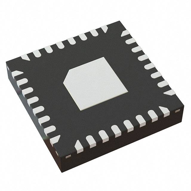


 工商网监
湘ICP备2023018690号
工商网监
湘ICP备2023018690号

