Product
Folder
Order
Now
Technical
Documents
Tools &
Software
Support &
Community
bq77908A
SLUSAV5A – FEBRUARY 2012 – REVISED OCTOBER 2014
bq77908A Multi-Cell Lithium-Ion/Polymer Precision Protector
1
1 Features
•
•
•
•
•
•
•
4-, 5-, 6-, 7-, or 8-Series Cell Protection
Individual Cell-Voltage Monitoring
Low-Side NMOS FET Drive for Charge and
Discharge Control
Compatible With 1-mΩ Current-Sense Resistor
Supply-Voltage Range From 5.6 V to 40 V
Integrated 3.3-V Micro-Power LDO Regulator
Low Supply Current
– Normal Mode: 50 µA, Typical
– Shutdown Mode, LDO OFF: 5 µA, Typical
•
•
38-Pin TSSOP Package
Internal 50-mA Automatic Cell Balancing
2 Applications
•
•
•
•
•
Cordless Power Tools
Cordless Lawn Equipment
Electric Bikes
UPS
Light Electric Vehicles (LEV)
3 Description
The bq77908A is a battery protection and cell balancing device intended for Li-Ion and Li-Polymer battery packs.
The bq77908A monitors 4- to 8-series individual cell voltages and provides fast-acting outputs that may be used
to drive N-channel MOSFETs to interrupt the power path. Activation delays and recovery methods for safety
conditions are fully programmable in non-volatile memory.
Automatic cell balancing is provided using internal 50-mA cell circuits. A robust balancing algorithm ensures
optimum performance by maintaining all cell voltages in balance. Balancing may be configured to operate at all
times, only during charge, or can be disabled completely.
Device Information(1)
PART NUMBER
PACKAGE
BODY SIZE (NOM)
bq77908A
TSSOP (38)
9.70 mm × 4.40 mm
(1) For all available packages, see the orderable addendum at the end of the data sheet.
WARNING
The bq77908A-series integrated circuit helps system designers greatly enhance
the safety of their Li-Ion and Li-Polymer battery packs when integrated
effectively and in accordance with the instructions detailed in this document by
technically qualified personnel familiar with battery pack application safety. This
data sheet must be read in its entirety before working with the bq77908A.
1
An IMPORTANT NOTICE at the end of this data sheet addresses availability, warranty, changes, use in safety-critical applications,
intellectual property matters and other important disclaimers. PRODUCTION DATA.
�bq77908A
SLUSAV5A – FEBRUARY 2012 – REVISED OCTOBER 2014
www.ti.com
Table of Contents
1
2
3
4
5
6
7
Features ..................................................................
Applications ...........................................................
Description .............................................................
Revision History.....................................................
Description (continued).........................................
Pin Configuration and Functions .........................
Specifications.........................................................
7.1
7.2
7.3
7.4
7.5
7.6
1
1
1
2
3
4
5
Absolute Maximum Ratings ...................................... 5
Handling Ratings....................................................... 6
Recommended Operating Conditions....................... 6
Thermal Information .................................................. 7
Electrical Characteristics........................................... 8
Serial Communication Interface (for Configuration
Only)......................................................................... 10
8
Detailed Description ............................................ 11
8.1
8.2
8.3
8.4
8.5
9
Overview .................................................................
Functional Block Diagram .......................................
Feature Description.................................................
Device Functional Modes........................................
Programming and Register Maps ...........................
11
11
11
25
26
Application and Implementation ........................ 37
9.1 Application Information............................................ 37
10 Device and Documentation Support ................. 52
10.1
10.2
10.3
10.4
Documentation Support ........................................
Trademarks ...........................................................
Electrostatic Discharge Caution ............................
Glossary ................................................................
52
52
52
52
11 Mechanical, Packaging, and Orderable
Information ........................................................... 52
4 Revision History
Changes from Original (February 2012) to Revision A
Page
•
Deleted the reference to medical equipment in the Applications section............................................................................... 1
•
Changed the minimum values for discharge and charge short circuit ................................................................................ 12
•
Added two table notes to Table 2......................................................................................................................................... 12
•
Added further detail to the DPCKN description .................................................................................................................... 13
•
Deleted an incorrect cross-reference label .......................................................................................................................... 15
•
Added a default to Discharge Overcurrent Detection Delay Settings ................................................................................. 31
•
Added new table notes ........................................................................................................................................................ 31
•
Added a new WARNING ..................................................................................................................................................... 31
•
Added a default to SCD Delay Settings .............................................................................................................................. 32
•
Changed the delay for 0000 in Charge Short-Circuit Delay-Time Settings.......................................................................... 33
•
Added a new table note ....................................................................................................................................................... 33
•
Changed the Cell-Balance Enable Control table ................................................................................................................. 34
•
Added application disclaimer note to the Application and Implementation section.............................................................. 37
2
Submit Documentation Feedback
Copyright © 2012–2014, Texas Instruments Incorporated
Product Folder Links: bq77908A
�bq77908A
www.ti.com
SLUSAV5A – FEBRUARY 2012 – REVISED OCTOBER 2014
5 Description (continued)
Additional advanced safety features of the bq77908A include the ability to control split power-path MOSFETs, an
open-cell sense-line detection mechanism, and the ability to detect an open or shorted external temperature
sensor fault condition.
Programmable Protection Functions
• Wide range of programmable detection thresholds and delay times
• Configurable for multiple cell types and application requirements:
– Cell overvoltage
– Cell undervoltage
– Pack discharge overcurrent
– Pack discharge short circuit
– Pack charge short-circuit current
• Variable gain (×1 or ×5) current-sense circuit
– Compatible with a wide range of current-sense resistors (1-mΩ to 5-mΩ typical) sized for application
requirements
Fixed Hardware Protection Functions
• Preset overtemperature protections
• Open-cell detection
• Open and shorted thermistor detection
• Brownout protection quickly shuts off FETs under low-battery conditions to minimize the risk of FET
overheating
Table 1. Device Comparison Table
PART NUMBER
PACKAGE TYPE
bq77908ADBT
TSSOP
PACKAGING
50-piece tube
bq77908ADBTR
TSSOP
2000-piece reel
Submit Documentation Feedback
Copyright © 2012–2014, Texas Instruments Incorporated
Product Folder Links: bq77908A
3
�bq77908A
SLUSAV5A – FEBRUARY 2012 – REVISED OCTOBER 2014
www.ti.com
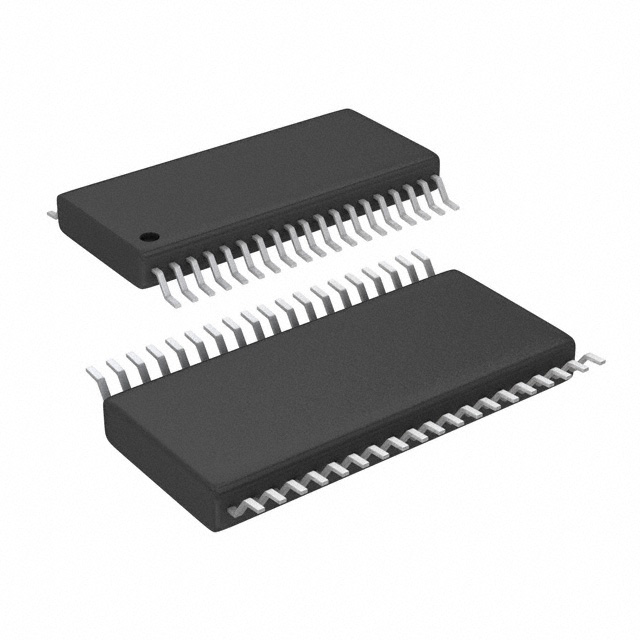
6 Pin Configuration and Functions
DBT PACKAGE
(TOP VIEW)
VC4
1
38
VC3
NC
2
37
NC
VC5
3
36
VC2
NC
4
35
NC
VC6
5
34
VC1
VC7
6
33
NC
VC8
7
32
NC
VC9
SENSE(–)
8
31
BAT
9
30
NC
SENSE(+)
10
29
VSS1
VSS2
11
28
EEPROM
VREG
12
27
SCLK
TS
13
26
SDATA
CHGST
14
25
GND
VTSB
15
24
GND
DCAP
16
23
GND
DSG
17
22
ZEDE
DPCKN
18
21
CHG
CPCKN
19
20
CCAP
P0034-05
Pin Functions
PIN
4
NAME
NO.
DESCRIPTION
BAT
31
Power supply voltage, tied to highest cell(+)
CCAP
20
Energy storage capacitor for charge FET drive
CHG
21
Charge FET (n-channel) gate drive
CHGST
14
Charger-status input, used to detect charger connection/wakeup
CPCKN
19
Pack—charger negative terminal (charger return)
DCAP
16
Energy storage capacitor for discharge FET drive
DPCKN
18
Pack—discharge negative terminal (load return)
DSG
17
Discharge FET (n-channel) gate drive
EEPROM
28
EEPROM programming voltage input. Connect to VSS for normal operation.
GND
23, 24, 25
NC
2, 4, 30, 32,
33, 35, 37
Logic ground (not for power return or analog reference). Tie to VSS.
No connect (DO NOT CONNECT) externally. Failure to leave NC pins open can cause faulty operation.
SCLK
27
Serial-communication clock input used for EEPROM programming
SDATA
26
Serial-communication data input/output used for EEPROM programming (open-drain)
SENSE(+)
10
Current-sense input
SENSE(–)
9
Current-sense input
TS
13
Temperature sensing input
VC1
34
Sense-voltage input terminal for most-positive cell
VC2
36
Sense-voltage input terminal for second-most-positive cell
VC3
38
Sense-voltage input terminal for third-most-positive cell
VC4
1
Sense-voltage input terminal for fourth-most-positive cell
VC5
3
Sense-voltage input terminal for fifth-most-positive cell
Submit Documentation Feedback
Copyright © 2012–2014, Texas Instruments Incorporated
Product Folder Links: bq77908A
�bq77908A
www.ti.com
SLUSAV5A – FEBRUARY 2012 – REVISED OCTOBER 2014
Pin Functions (continued)
PIN
DESCRIPTION
NAME
NO.
VC6
5
Sense-voltage input terminal for sixth-most-positive cell
VC7
6
Sense-voltage input terminal for seventh-most-positive cell
VC8
7
Sense-voltage input terminal for eighthmost-positive (most-negative) cell
VC9
8
Most-negative cell(–) terminal (BAT–)
VREG
12
Integrated 3.3-V regulator output
VSS1
29
Analog ground (substrate reference)
VSS2
11
Analog ground (substrate reference)
VTSB
15
Thermistor bias supply (sourced from VREG)
ZEDE
22
Zero Delay test mode pin. Enables serial communications interface and minimizes protection delay times
when connected to logic high. Connect to VSS for normal operation. A strong connection is
recommended.
7 Specifications
7.1 Absolute Maximum Ratings (1)
Over-operating free-air temperature range (unless otherwise noted)
MIN
DC supplyvoltage
range, VMAX
–0.3
BAT
CPCKN
(BAT – 50)
(BAT + 0.9) V
V
–0.3
9
V
SENSE(+)
–3
3
V
SENSE(–)
–0.3
50
V
SCLK, SDATA, ZEDE (2)
–0.3
7
V
TS, CHGST (3) (4)
–0.3
BAT
V
EEPROM
–0.3
15
V
(9 – x) × 5
3
V
CHG referenced to CPCKN
– 0.3
15
V
DSG referenced to VSS
–0.3
15
V
VTSB
–0.3
5
Storage temperature range, Tstg
(4)
V
–3
70
Regulator current, IREG
(3)
V
V
Current for cell balancing, ICB
(2)
(5 × N) V, N =
number of cells
implemented in pack
50
Cell input VC9
(1)
UNIT
–0.3
Cell input VCx, x = 1–8
Output
voltage
range, VO
MAX
DPCKN
Cell-to-cell differential, VCx to VC(x+1), x = 1 to 8
Input voltage
range, VIN
TYP
45
–65
V
mA
mA
150
°C
Stresses beyond those listed under Absolute Maximum Ratings may cause permanent damage to the device and expose the system to
potential safety risks, resulting from the damage to the IC. These are stress ratings only. Functional operation of the device at these or
any other conditions beyond those indicated under Recommended Operating Conditions is not implied. Exposure to absolute-maximumrated conditions for extended periods may affect device reliability or cause damage to the device.
All signal/logic pins that may be connected to the pack external terminals are internally clamped to a maximum voltage of 5 V. If the
external source driving these signals exceeds the clamp threshold, series resistance from the pin to the pack terminal is required to
avoid overstress on the clamping circuit.
CHGST and TS pins are tolerant of applied overvoltage as noted to allow for charger single-fault tolerance. Normal operating range is
typically 3.3 V or less at this pin; thus, high voltage seen here may correspond to a fault condition.
Although no damage results when CHGST = VSS – 0.3 V, for proper operation at power up, CHGST must be ≥ VSS – 0.25 V.
Submit Documentation Feedback
Copyright © 2012–2014, Texas Instruments Incorporated
Product Folder Links: bq77908A
5
�bq77908A
SLUSAV5A – FEBRUARY 2012 – REVISED OCTOBER 2014
www.ti.com
7.2 Handling Ratings
TSTG
Storage temperature range
MAX
–65
150
°C
2
kV
500
V
110
°C
Human body model (HBM) ESD stress voltage (1)
ESD Rating
Charged device model (CDM) ESD stress voltage (2)
TFUNC
(1)
(2)
MIN
Functional Temperature
–40
UNIT
JEDEC document JEP155 states that 500-V HBM allows safe manufacturing with a standard ESD control process.
JEDEC document JEP157 states that 250-V CDM allows safe manufacturing with a standard ESD control process.
7.3 Recommended Operating Conditions
Over-operating free-air temperature range (unless otherwise noted)
MIN
Supply voltage
BAT (1)
Cell differential, VCx to VC(x + 1),
(x = 1 to 8 )
VI
Input voltage range
VIH
Logic-level input, high
VIL
Logic-level input, low
TYP
UNIT
35 (3)
V
1.4
4.375
(9 – x) ×
4.375 V
Cell input VCx, x = 1 – 8
Cell input VC9
VSENSE(+)
MAX
5.6 (2)
SCLK, SDATA, EEPROM, ZEDE
–1
V
1
0.8 × VREG
V
0.2 × VREG
V
VSS – 1
VSS + 1
V
–0.2
BAT
V
1000
Ω
VSENSE(–)
Voltage applied at SENSE(±)
pins
RVCX
Recommended VCx nominal
input resistance
IREG
Regulator current
10
mA
ICB
Cell balancing current
50
mA
CVCX
Recommended VCx nominal
input filter capacitance
1
µF
RCPCKN,
RDPCKN
Recommended isolation-pin
input resistance
100
Ω
RLDRM_DET
Pulldown for load-removal
detection
50
kΩ
CVREG
External 3.3-V REG capacitor
50
100
1
µF
EEPROM number of writes
3
times
TOPR
Operating temperature
Meeting all specification limits
–25
85
°C
TFUNC
Functional temperature
Operational but may be out of spec limits,
no damage to part
–40
100
°C
CCCAP,
CDCAP
External capacitance on CCAP
and DCAP pins (4)
RP
Serial communication interface
SCLK, SDATA
pullup resistance (5)
(1)
(2)
(3)
(4)
(5)
0.1
1
µF
2.2
kΩ
The voltage rate of change at the BAT pin should be limited to a maximum of 1 V per µs in order to prevent unwanted device shutdown.
Minimum voltage assumes 4-cell connection at 1.4 V/cell.
Maximum voltage assumes 8-cell connection at 4.375 V/cell.
CCCAP and CDCAP act as charge reservoirs for the CHG and DSG pins when driving large protection FETs. Minimum value is required
for stability, independent of the CHG and DSG loading.
Pullups for configuration of device during pack manufacturing. SCLK and SDATA should be pulled high or low in application.
NOTE
Refer to the Open-Cell Detection overview in the Application Information section for a
description of RVCX and CVCX sizing.
6
Submit Documentation Feedback
Copyright © 2012–2014, Texas Instruments Incorporated
Product Folder Links: bq77908A
�bq77908A
www.ti.com
SLUSAV5A – FEBRUARY 2012 – REVISED OCTOBER 2014
7.4 Thermal Information
bq77908A
THERMAL METRIC (1)
DBT
UNIT
38 PINS
Junction-to-ambient thermal resistance, non-LDO (2)
θJA
(2) (3)
71.7
°C/W
θJA2
Junction-to-ambient thermal resistance, LDO
115.8
°C/W
θJCtop
Junction-to-case (top) thermal resistance (4)
18.5
°C/W
θJB
Junction-to-board thermal resistance (5)
33.9
°C/W
ψJT
Junction-to-top characterization parameter, non-LDO
ψJT2
Junction-to-top characterization parameter, LDO (6)
ψJB
θJCbot
(1)
(2)
(3)
(4)
(5)
(6)
(7)
(8)
(6)
1
°C/W
38.9
°C/W
Junction-to-board characterization parameter (7)
33.2
°C/W
(8)
N/A
°C/W
Junction-to-case (bottom) thermal resistance
(3)
For more information about traditional and new thermal metrics, see the Semiconductor and IC Package Thermal Metrics application
report (SPRA953).
The junction-to-ambient thermal resistance under natural convection is obtained in a simulation on a JEDEC-standard, high-K board, as
specified in JESD51-7, in an environment described in JESD51-2a.
These metrics should be used only for calculating junction temperature due to power dissipation resulting from the IOUT load on VREG.
Junction temperature calculations for all other sources of power dissipation should use the standard values θJA and ψJT.
The junction-to-case (top) thermal resistance is obtained by simulating a cold plate test on the package top. No specific JEDECstandard test exists, but a close description can be found in the ANSI SEMI standard G30-88.
The junction-to-board thermal resistance is obtained by simulating in an environment with a ring cold plate fixture to control the PCB
temperature, as described in JESD51-8.
The junction-to-top characterization parameter, ψJT, estimates the junction temperature of a device in a real system and is extracted
from the simulation data for obtaining RθJA, using a procedure described in JESD51-2a (sections 6 and 7).
The junction-to-board characterization parameter, ψJB, estimates the junction temperature of a device in a real system and is extracted
from the simulation data for obtaining RθJA, using a procedure described in JESD51-2a (sections 6 and 7).
The junction-to-case (bottom) thermal resistance is obtained by simulating a cold plate test on the exposed (power) pad. No specific
JEDEC standard test exists, but a close description can be found in the ANSI SEMI standard G30-88.
Spacer
Submit Documentation Feedback
Copyright © 2012–2014, Texas Instruments Incorporated
Product Folder Links: bq77908A
7
�bq77908A
SLUSAV5A – FEBRUARY 2012 – REVISED OCTOBER 2014
www.ti.com
7.5 Electrical Characteristics
VCELL(n) = 1.4 to 4.375 for all cells, TA = –25°C to 85ºC, BAT = 5.6 to 35 V; Typical values stated where TA = 25°C and BAT =
28.8 V (unless otherwise noted)
PARAMETER
TEST CONDITIONS
MIN
TYP
MAX
UNIT
50
75
µA
VCELL< VUV, VREG = off (EEPROM set), CPCKN = 0.3 V
5
17
VCELL < VUV, VREG = off (EEPROM set), CPCKN = 0.5 V
20
60
SUPPLY CURRENT
ICC
NORMAL-mode average supply current
ISHUTDOWN_2 (1)
SHUTDOWN mode, LDO off
CHG, DSG = on (no dc load), VREG = on,
IREG = 0 mA, BAT = 28.8 V
µA
INTERNAL POWER CONTROL (STARTUP, SHUTDOWN, GATE DRIVE UNDERVOLTAGE)
Minimum voltage for initial power up (2)
Measured at BAT pin
LDO POR voltage – voltage on LDO that
initiates a POR
ILDO = 2 mA
2.7
VGATE_UV
FET gate shutdown threshold (voltage falling)
Measured at CCAP/DCAP pins
4.5
VGATE_UV_H
FET gate shutdown hysteresis voltage
Measured at CCAP/DCAP pins
0.45
VSTARTUP
VPOR
(3)
4.9
7
V
3.2
V
5.3
V
0.7
V
FET DRIVE (4)
V(FETON)
V(FETOFF)
Gate drive voltage at DSG and CHG pins for
FET ON (enabled) conditions
Gate drive voltage at DSG and CHG pins for
FET OFF (disabled) conditions
BAT voltage = 35 V (gate-drive circuit in regulation mode),
no dc load
11
BAT voltage = 10 V (gate-drive circuit in dropout mode), no
dc load
9
BAT voltage = 6.4 V (gate-drive circuit in dropout mode), no
dc load
>VGATE_UV
V
0.2
VO(FETOFFCHG) = V(VHG) – Vpack–
0.2
Rise time, measured at IC pin (CHG or DSG)
CL = 50 nF, BAT = 6.4 V
CL = 50 nF, BAT = 35 V
tf
14
VO(FETOFFDSG) = V(DSG) – VGND
CL = 50 nF, BAT = 35 V
tr
12
Fall time, measured at IC pin (CHG or DSG)
CL = 50 nF, BAT = 6.4 V
V
VDSG: 10% to 90%
90
140
VCHG: 10% to 90%
90
140
VDSG: 10% to 90%
90
140
VCHG: 10% to 90%
90
140
VDSG : 90% to 10%
10
20
VCHG: 90% to 10%
20
40
VDSG : 90% to 10%
50
100
VCHG: 90% to 10%
50
100
µs
µs
VREG, INTEGRATED 3.3-V LDO
VREG
Output-voltage regulation under all line, load,
temperature conditions
ISC
Short-circuit current limit
(1)
(2)
(3)
(4)
(5)
(6)
8
IOUT = 10 mA (maximum dc load) (5)
3.1
3.3
3.55
IOUT = 0.2 mA
3.1
3.3
3.55
V
VREG = 0 V, forced external short (thermally protected) (6)
20
45
mA
V
For predictable shutdown current, the voltage at CPCKN with respect to VSS must be controlled. In the parallel FET case, CPCKN is
clamped through the body diode of the charge FET. In the series FET case, external circuitry is required to keep CPCKN from floating.
Contact TI for recommended application circuits.
At this voltage, the LDO has sufficient voltage to maintain regulation. The POR then enables the charger-detect logic. Logic is held in
reset until inserted into charger and LDO has reached VPOR. The part still operates below 7 V to the spec limit of 5.6 V.
VPOR and VREG are derived from the same internal reference, so that the MAX value of VPOR and the MIN value of VREG do not occur
at the same time.
FET drive is disabled if voltage at CCAP or DCAP pins < VGATE_UV. Turnoff due to gate-drive undervoltage condition meets the same
timing requirements as logic-initiated gate turnoff.
Electrical Characteristics assume that IOUT = 0 so that the internal junction temperature (TJ) is effectively equal to the ambient
temperature (TA). For larger non-zero values of IOUT, TJ can be significantly higher than TA. In these cases, TJ should be substituted for
TA in the test and operating conditions. TJ can be calculated from the device power dissipation as described under Thermal
Characteristics. The device power dissipation due to IOUT is (VBAT – VREG) × IOUT.
Regulator shuts down prior to current-limit maximum specification if junction temperature exceeds safe range.
Submit Documentation Feedback
Copyright © 2012–2014, Texas Instruments Incorporated
Product Folder Links: bq77908A
�bq77908A
www.ti.com
SLUSAV5A – FEBRUARY 2012 – REVISED OCTOBER 2014
Electrical Characteristics (continued)
VCELL(n) = 1.4 to 4.375 for all cells, TA = –25°C to 85ºC, BAT = 5.6 to 35 V; Typical values stated where TA = 25°C and BAT =
28.8 V (unless otherwise noted)
PARAMETER
TEST CONDITIONS
MIN
TYP
MAX
UNIT
TS TEMPERATURE SENSING
VTSB pin pullup resistance
IOUT = –1 mA at VTSB pin, rDS(on) = (VREG – VVTSB) / 1 mA
50
150
TS pin fault-signal pulldown resistance
OV_TS_CTRL = 1, VCELL > VOV
50
150
ITS_PD
TS pin thermistor check pulldown current
TS = 3.3 V (externally driven)
2
4
µA
tTHERM_CHECK
Thermistor fault sampling interval
VEXT_BIAS_DET
Thermistor external-bias supply-detection
threshold
Internal VTSB supply off
13%
17%
VREG
VHOT
Overtemperature-detection threshold
(ratiometric to VTSB)
Internal VTSB supply on, no external bias
17%
21%
VREG
VTH_SHORT
Thermistor short-detection trip threshold
(ratiometric to VTSB)
Internal VTSB supply on, no external bias
1%
10%
VREG
VTH_HYST
TS comparator hysteresis
Hysteresis for short, open, and overtemperature
comparators
3%
8%
VREG
VTH_OPEN
Thermistor open detection (ratiometric to
VTSB)
Internal VTSB supply on, no external bias
90%
98%
VREG
Cell-balance internal resistance (7)
rDS(on) for internal FET
switch, TA = 0°C to 50°C
rDS(on)
Ω
1
4
15%
s
CELL BALANCE
RBAL
tCELL_BAL_CHECK
VCELL = CBVMAX = 3.9
–50%
10
50%
VCELL = CBVMAX = 3.2
–50%
20
50%
VCELL = CBVMAX = 2.5
–50%
30
50%
Cell balancing update interval
7.5
Ω
min
OPEN-CELL CONNECTION
ILOAD_OPEN_CELL (8)
Cell loading during open-cell detect
tOPEN_CELL_CHECK
Open-cell fault-sampling interval
(N = total number of cells in pack)
ROPEN_CELL
Minimum impedance from cell terminal to VCx
input that is interpreted as an open condition
BATTERY-PROTECTION-THRESHOLD TOLERANCES
75
450
4×N
s
100
kΩ
(9)
OV detection threshold accuracy for VOV = 4.2
V (10)
TA = 0°C to 50°C
–25
25
TA = –25°C to 85°C
–50
50
OV detection threshold accuracy for VOV = 3.2
V (10)
TA = 0°C to 50°C
–50
50
TA = –25°C to 85°C
–75
75
ΔVUV
UV detection threshold accuracy
TA = –25°C to 85°C
–100
100
ΔVSCD
ΔVOCD
OCC/SCD detection threshold accuracy
TA = –25°C to 85°C
–20%
20%
ΔVOV
ΔVSCC
µA
SCC detection threshold accuracy
VSCC from 10 mV to 15 mV
VSCC > 15 mV
mV
–3
3
–20%
20%
mV
mV
BATTERY PROTECTION DELAY-TIME TOLERANCES (9)
ΔtOV
OV detection delay time accuracy
–15%
15%
ΔtUV
UV detection delay time accuracy
–15%
15%
ΔtSCD
OCD/SCD detection delay time accuracy
–15%
15%
ΔtSCC
SCD detection delay time accuracy
–15%
15%
Default EEPROM setting
tSCD Max
(7)
Balance current is not internally limited. External series resistance must be used to ensure balance current is below 50 mA maximum to
limit IC internal power dissipation.
(8) This current is sufficient to detect an open-cell condition down to 100 kΩ across the cell from circuitry outside of the bq77908A. The
average current from this loading is less than 1 µA for a 8-cell configuration.
Application Note: When using this part with other devices that connect to the battery cells, care must be taken to avoid excessive
parallel capacitances on the cell input pins.
(9) Nominal values are set by EEPROM programming; see EEPROM table for possible values.
(10) Standard production parts are calibrated at 4.2 V. An additional OV threshold accuracy shift of 25 mV per volt of OV set point is
possible. Contact TI for calibration options at set point voltages other than 4.2 V.
Submit Documentation Feedback
Copyright © 2012–2014, Texas Instruments Incorporated
Product Folder Links: bq77908A
9
�bq77908A
SLUSAV5A – FEBRUARY 2012 – REVISED OCTOBER 2014
www.ti.com
Electrical Characteristics (continued)
VCELL(n) = 1.4 to 4.375 for all cells, TA = –25°C to 85ºC, BAT = 5.6 to 35 V; Typical values stated where TA = 25°C and BAT =
28.8 V (unless otherwise noted)
PARAMETER
TEST CONDITIONS
MIN
TYP
MAX
UNIT
5.6 V < BAT < 35 V
0.3
0.5
0.7
V
CHARGER DETECTION (11)
Voltage at CHGST pin, referenced to VSS, to
determine charger present (charger insertion
detected when voltage at CHGST pin >
VCHG_DET1)
VCHG_DET1
LOAD REMOVAL DETECTION
VOPEN_LOAD
Voltage at DPCKN, referenced to VSS, with
DSG FET disabled to detect load removal
(load removal detected when voltage at
DPCKN < VOPEN_LOAD)
5.6 V < BAT < 35 V
1.5
2
2.5
V
RDSG_GND
Internal resistance between DPCKN and VSS
5.6 V < BAT < 35 V
1000
1500
3000
kΩ
Data retention
5.6 V < BAT < 35 V
10
EEPROM LIFETIME
TDR
years
(11) Alternate charger detection options are available using the CPCKN pin. Contact TI for additional configuration versions.
7.6 Serial Communication Interface (for Configuration Only)
BAT = 5.6 V to 35 V, TA = –25°C to 85°C
PARAMETER
MIN
MAX
UNIT
tr
SCLK, SDATA rise time
1000
ns
tf
SCLK, SDATA fall time
300
ns
tw(H)
SCLK pulse duration, high
tw(L)
tsu(STA)
th(STA)
START condition hold time after which the first clock pulse is generated.
tsu(DAT)
th(DAT)
8
µs
SCLK pulse duration, low
10
µs
Setup time for START condition
9.4
µs
8
µs
Data setup time
250
ns
Data hold time
0
µs
tsu(STOP)
Setup time for STOP condition
8
µs
tsu(BUF)
Time the bus must be free before new transmission can start
9.4
µs
tV
Clock low to data out valid
th(CH)
Data out hold time after clock low
0
fSCL
Clock frequency
0
900
ns
50
kHz
ns
tsu(BUF)
10
Submit Documentation Feedback
Copyright © 2012–2014, Texas Instruments Incorporated
Product Folder Links: bq77908A
�bq77908A
www.ti.com
SLUSAV5A – FEBRUARY 2012 – REVISED OCTOBER 2014
8 Detailed Description
8.1 Overview
The bq77908A battery protection and cell balancing device for Li-Ion and Li-Polymer battery packs monitors 4- to
8-series individual cell voltages and provides fast-acting outputs that may be used to drive N-channel MOSFETs
to interrupt the power path. Activation delays and recovery methods for safety conditions are fully programmable
in non-volatile memory.
Automatic cell balancing is provided using internal 50-mA cell circuits. A robust balancing algorithm ensures
optimum performance by maintaining all cell voltages in balance. Balancing may be configured to operate at all
times, only during charge, or can be disabled completely.
8.2 Functional Block Diagram
BAT
VC1
VREG
3.3-V LDO
VC2
POR / STARTUP UVLO
VTSB
MULTI-LEVEL
TEMP
COMPARATOR
VC3
TS
VC4
VCELL
X
_
VC5
PROGRAMMABLE
DELAY
PROGRAMMABLE
UV COMPARATOR
EEPROM
1 mA
CELL
SELECTION
SWITCHES
VC6
NTC/ Charger
Disable
PROGRAMMABLE
OV COMPARATOR
Thermistor
Check
PROGRAMMABLE
DELAY
VC7
CELL SAMPLING SELECTION CONTROL
(1–8)
VC8
VC9
SENSE(+)
SENSE(–)
SCLK
2
CONTROL
LOGIC
I C SERIAL
INTERFACE
SDATA
EEPROM R/W
PROGRAMMABLE
DISCHARGE
OVERCURRENT
COMPARATOR
EEPROM
TESTMODE
CONTROL
PROGRAMMABLE
DELAY
ZEDE
COMP
PROGRAMMABLE
DISCHARGE
SHORT CIRCUIT
COMPARATOR
PROGRAMMABLE
DELAY
PROGRAMMABLE
CHARGE SHORT
CIRCUIT
COMPARATOR
PROGRAMMABLE
DELAY
CHGST
WAKE-UP
CIRCUIT
COMP
OC / SC
RECOVERY
CIRCUIT
COMP
VSS
DSG FET
NMOS DRIVER
DCAP DSG
CHG FET
NMOS DRIVER
DPCKN CCAP CHG
CPCKN
8.3 Feature Description
8.3.1 Programmable Protection Functions
The bq77908A provides the following types of protection functions:
• Cell overvoltage
• Cell undervoltage
• Discharge overcurrent
• Discharge-current short circuit
• Charge-current short circuit
Submit Documentation Feedback
Copyright © 2012–2014, Texas Instruments Incorporated
Product Folder Links: bq77908A
11
�bq77908A
SLUSAV5A – FEBRUARY 2012 – REVISED OCTOBER 2014
www.ti.com
Feature Description (continued)
All of the voltage/current and time-delay thresholds can be adjusted for a specific application by programming the
EEPROM settings of the IC. The ranges available are shown in Table 2.
CAUTION
Only a maximum of three EEPROM write cycles per byte should performed to ensure
long-term data retention stability. (For circuit development purposes, the EEPROM
may be rewritten many times.)
Table 2. Detection Voltage, Detection Delay Time Summary
PARAMETER
Overvoltage
RANGE
(EEPROM Selected)
MIN
MAX
STEP
Cell voltage
2.8 V
4.375 V
25 mV
Delay
0.5 s
2.25 s
0.25 s
Hysteresis
0 mV
300 mV
25 mV or 50 mV
Cell voltage
Undervoltage
Delay
Hysteresis
SENSE(–) pin voltage with
respect to SENSE(+)
Discharge overcurrent
Discharge short circuit
Delay (2)
Charge short circuit
SENSE(–) pin voltage with
respect to SENSE(+)
100 mV
32 s
Binary spacing
400 mV
1600 mV
400 mV
25 mV
100 mV
5 mV
High
125 mV
500 mV
25 mV
20 ms
300 ms
20 ms
400 ms
2000 ms
100 ms
Low
40 mV
190 mV
10 mV
High
200 mV
950 mV
50 mV
Fast
120 µs
960 µs
60 µs
Slow
50 ms
1500 ms
50 ms or 100 ms
Low
–10 mV
–85 mV
5 mV
High
–50 mV
–425 mV
25 mV
120 µs
960 µs
60 µs
Delay
(1)
(2)
2.9 V
Low
Delay (1)
SENSE(–) pin voltage with
respect to SENSE(+)
1.4 V
500 ms
If cell balancing during discharge is enabled, then the maximum permitted delay setting is 180 ms.
If cell balancing during discharge is enabled, then the maximum permitted delay setting is 100 ms.
8.3.1.1 Cell Overvoltage Detection and Recovery
The CHG FET is turned off if any one of the cell voltages remains higher than VOV for a period greater than tOV.
As a result, the cells are protected from an overcharge condition. After an overvoltage event occurs, the all cells
must relax to less than (VOV – VHYST) to allow recovery.
The VOV, tOV, and VHYST values can be set via the EEPROM bits OVT, OVD, and OVH.
8.3.1.2 Cell Undervoltage Detection and Recovery
When any one of the cell voltages falls below VUV, for a period of tUV, the bq77908A enters the undervoltage
protection state. The DSG FET is turned off, and depending on configuration, the device could enter the
SHUTDOWN mode. Both VUV and tUV can be configured via EEPROM bits UVT and UVD.
The recovery (fault release) is controlled by the EEPROM configuration bit UV_REC.
If UV_REC = 0, the DSG FET is re-enabled when all the cell voltages increase back above the VUV threshold
level plus the hysteresis value; there is no time-delay part of the recovery. In this case, when UV_REC = 0 and
under high load currents, the VCELL voltages could recover to >UV + hyst very quickly, re-enabling the FETs and
allowing the high load current to persist. Care should be taken when using this UV_REC = 0 mode, as the power
MOSFETs could oscillate rapidly.
12
Submit Documentation Feedback
Copyright © 2012–2014, Texas Instruments Incorporated
Product Folder Links: bq77908A
�bq77908A
www.ti.com
SLUSAV5A – FEBRUARY 2012 – REVISED OCTOBER 2014
WARNING
To minimize application safety risk, care should be taken to properly set
overcurrent and cell undervoltage trip thresholds, because it is possible that a
fully charged pack with a continuous high discharge load can oscillate in and
out of the undervoltage condition. This may result in overheating of the cells or
protection MOSFETs due to the potentially high-duty-cycle operation.
If UV_REC = 1, the DSG FET is re-enabled when all the cell voltages increase back above the VUV threshold
level plus the hysteresis value AND the load is removed.
Current is interrupted by opening the FETs, and at this point the cell voltages may quickly recover above the UV
+ hyst levels if the battery pack is not completely depleted. However, the external load may remain attached.
When the external load is removed, the IC detects load removal and reconnects the DSG FET.
If UV_REC_DLY = 1 and any cell remains below the VUV threshold level plus the hysteresis for longer than 8
seconds, the device enters SHUTDOWN mode. If UV_REC_DLY = 0, the device does not enter the
SHUTDOWN mode from the cell undervoltage fault condition.
The LDO is turned off during the SHUTDOWN mode. Insertion into a charger is required to recover from the
SHUTDOWN mode.
Charger detection methods are discussed in later sections, such as Application Information.
8.3.1.3 Overcurrent in Discharge (OCD) Detection
The OCD detection feature senses an overload current by measuring the voltage across the sense resistor.
When an overload condition is detected, both of the power FETS are disabled to prevent damage to the cells and
FET components. Criteria for fault recovery depend on the state of the SOR (EEPROM bit). Overcurrent trip level
(VOCD) and blanking time delay (tOCD) are programmable via EEPROM bits OCDT and OCDD to match individual
application requirements.
8.3.1.4 Short Circuit in Discharge (SCD) Detection
The SCD detection function senses severe discharge current by measuring the voltage across the sense
resistor. When a short circuit is detected, both of the power FETs are disabled to prevent damage to the cells
and FET components. Criteria for fault recovery depend on the state of the of the SOR (EEPROM bit). Shortcircuit trip level (VSCD) and blanking time delay (tSCD) are programmable via EEPROM bits SCDT and SCDD to
match individual application requirements.
8.3.1.5 Load Removal Detection/OCD and SCD Fault Recovery
The part includes an internal high-impedance connection between the DPCKN and VSS pins of approximately
1.5 MΩ. An external load (for example power tool motor winding), if still connected to the pack terminals, would
present a very low impedance relative to the high internal pulldown resistance.
NOTE
If the external load presents additional capacitance, then an external pulldown may be
required between the DPCKN and VSS pins. This extra pulldown does not increase
battery load current when the external load is removed.
If the DSG power FET is disabled after an overload or short-circuit event, the voltage at the DPCKN is
approximately equivalent to the BAT voltage potential while an external load (for example, power tool motor) is
present at the pack terminals. When the external load is removed, the high-value internal resistance pulls down
the DPCKN potential to the internal VSS level. An internal comparator monitors the DPCKN terminal voltage
during the protection state. DPCKN must rise above VOPEN_LOAD within approximately 75 µs for the load to be
detected. When the DPCKN voltage falls to < VOPEN_LOAD (approximately 2 V), the load removal is detected. Fault
recovery from an OCD or SCD event depends on the state of the SOR EEPROM bit.
If SOR = 0, the FETs are re-enabled only after the external load removal is detected.
If SOR = 1, the FETs are re-enabled after the load is removed and a charger insertion is detected.
Submit Documentation Feedback
Copyright © 2012–2014, Texas Instruments Incorporated
Product Folder Links: bq77908A
13
�bq77908A
SLUSAV5A – FEBRUARY 2012 – REVISED OCTOBER 2014
www.ti.com
(Details of charger presence detection methods are discussed in later sections.)
8.3.1.6 Short Circuit in Charge (SCC) Detection
The SCC detection function senses severe charge current by measuring the voltage across the sense resistor. In
this case, the voltage is negative (opposite polarity of OCD and SCD detection). When a short circuit is detected,
both of the power FETS are disabled to prevent damage to the cells and FET components. Short-circuit trip level
(VSCD) and blanking time delay (tSCD) are programmable via EEPROM bits SCCT and SCCD to match individual
application requirements.
NOTE
The current sensing element must be located along a common charge and discharge path
in order to protect against both charge and discharge current faults. This is particularly
important to note for parallel FET configurations or configurations that combine the FET
with the sense element.
8.3.1.7 Short Circuit in Charge Recovery
An SCC fault is cleared after charger removal is detected. (See later sections for details of charger insertion and
removal detection methods.)
8.3.2 Fixed Hardware Fault-Protection Functions
The bq77908A provides a number of fixed protection settings for hardware faults as listed:
• Open-cell connection
• Pack voltage Brownout condition—power FET protection
• Charger-enable temperature range
• Open thermistor connection
• Shorted thermistor connection
• Overtemperature protection
8.3.2.1 Open-Cell Connection
A mechanical or assembly fault in the pack can cause a high-impedance or broken connection between the IC
cell sense pins and the actual cells. During operation, the bq77908A periodically checks the validity of the
individual cell voltage reading by applying a micropower pulsed load across each cell. If the connection between
the pin and the cell is opened, the apparent cell voltage will collapse and a fault (permanent failure) condition is
detected. The open-cell detection reading is taken at a time interval of tOPEN_CELL_CHECK, as specified in the
parametric tables. Recommended external filter-capacitor maximum value is also listed in the Recommended
Operating Conditions. Because an open-cell fault may be considered as a permanent failure, the fault detection
logic must detect two consecutive open-cell conditions prior to activating the protection condition for an open-cell
fault. Due to the nature of open-cell fault conditions, other apparent faults may be observed during an open-cell
condition.
Summary of open-cell detection-logic operation:
• For an N-cell battery pack, the bq77908A always protects (by opening the FETs) in some manner within the 2
× N × tOPEN_CELL_CHECK time frame (sampling interval is tOPEN_CELL_CHECK, and two successive open-cell faults
are required to avoid nuisance tripping).
• Because an open-cell connection results in a floating VCx input, a UV or an OV fault may be detected before
the open-cell fault due to their shorter fault filter times. Furthermore, the OV or UV condition may not be
stable and the fault may recover during the open-cell check interval (that is, the FETs may toggle). In all
cases the open-cell fault is detected within the open-cell fault filter time and the FETs are shut off until the
recovery conditions are satisfied.
• The LDO shuts down following the detection of an open-cell fault, provided that a charger is not detected.
When the pack is awakened following this, the open-cell fault is initially cleared (FETs closed) and must be
re-evaluated over the filter time before the fault is again registered. Charger detection inhibits LDO shutdown;
however, once the charger is disconnected, the LDO then shuts down, provided that the recovery conditions
have not yet been satisfied.
14
Submit Documentation Feedback
Copyright © 2012–2014, Texas Instruments Incorporated
Product Folder Links: bq77908A
�bq77908A
www.ti.com
SLUSAV5A – FEBRUARY 2012 – REVISED OCTOBER 2014
8.3.2.2 Additional Fault Protection Functions
The brownout protection functionality is discussed in the IC Internal Power Control section of this document.
Thermistor fault detection, charger/thermistor interface and control are discussed in the Application Information
section.
8.3.3 IC Internal Power Control
8.3.3.1 Power-On Reset/UVLO
On initial application of power to the BAT pin, the IC internal power supply rail begins to ramp up. The IC
contains an internal undervoltage lockout (UVLO)/power-on reset (POR) circuit that prevents operation until the
BAT voltage is sufficient to ensure predictable start-up and operation. All power for the IC internal circuitry is
derived from the BAT pin. The UVLO/POR start-up threshold is specified in the parametric table as VSTARTUP.
Once the BAT voltage has exceeded this level, the internal LDO regulator and control circuitry are enabled and
continue to operate even if BAT falls below VSTARTUP. If the BAT pin falls below the operational range given
under Recommended Operating Conditions, the device powers down.
On initial power up, the state of the output MOSFET drive pins (CHG and DSG) is indeterminate until the voltage
on BAT reaches the VSTARTUP threshold. No load should be applied during this period.
8.3.3.2 BAT Holdup/Brownout Protection Functionality
The BAT pin is used to power the IC internal circuitry, and should be supplied through a diode and held up with a
capacitor placed near the IC as shown in the application diagrams (see Figure 2). The external diode prevents
discharge of the IC power rail during external transients on the PACK(+) node.
This allows the bq77908A to maintain proper control of the pack and system during brownout conditions.
Brownout is defined as a situation during which the stack voltage collapses to a voltage below the minimum
operating voltage of the IC (~5.6 V) for a short duration (~1 s). A typical application case is shown below.
Additional examples are provided in the Application Information section later in this document.
If there are short-duration sags in the PACK(+) voltage (typically due to high load transients), the operating
current for the IC is momentarily provided by the external capacitor. Assuming that there is no external load on
the VREG (LDO output) pin, the IC draws approximately 50-µA average current from the capacitor. The holdup
time before the IC goes into SHUTDOWN mode depends on the initial pack voltage. For a normal low battery
initial condition using a 4-cell stack, the cells may be in the range of 3 V/cell or 12 V total for the pack voltage. If
a load transient occurs at this point, and the pack voltage sags down to below the IC POR threshold, the voltage
at the BAT pin is held above 5 V for slightly greater than one second using a 10-µF capacitor.
Waveforms typical of a load transient during low pack voltage conditions are shown as follows. In the first load
transient, the PACK(+) rail momentarily collapses but the load is disconnected before the holdup time limit is
exceeded. In the second load transient, the load is left on for a duration exceeding the holdup capability, so when
the IC operating voltage reaches the gate-drive undervoltage limit, the external power FETs are disabled to
disconnect the load.
Submit Documentation Feedback
Copyright © 2012–2014, Texas Instruments Incorporated
Product Folder Links: bq77908A
15
�bq77908A
SLUSAV5A – FEBRUARY 2012 – REVISED OCTOBER 2014
www.ti.com
Load Disconnect (Gate Drive Shutoff)
80
I_LOAD
60
40
20
14
12
V_PACK(+)
10
8
Minimum
Operating
Voltage
(5.6 V)
6
4
14
12
10
V_BAT
(at IC PIN) 8
6
4
T_holdup ~ 1 s
Minimum
Operating
Voltage
(5.6 V)
Time (s)
Figure 1. Load Transient Examples
8.3.3.3 BAT Voltage Peak Detection/Transient Suppression
The use of an external diode and holdup capacitor allows the IC to provide controlled operation during brownout
conditions. However, when the battery pack is at a high level, a different issue must be considered.
During normal operation of power equipment, load transients may induce high-voltage pulses on the PACK(+) rail
that exceed the steady-state dc voltage output of the battery pack. In some cases, these transient voltages can
exceed the battery rail by several volts. The voltage at the BAT pin may be held up to these higher voltages for a
longer duration because the diode prevents the capacitor from discharging back into the cell stack after the
transient pulses decay. When the dc level of the battery pack voltage is near 35 Vdc, high-current load
disconnection may cause transients that would exceed the absolute maximum ratings of the device.
The BAT pin incorporates an internal Zener clamp that dissipates any transient voltage at the BAT pin that
exceeds 50 V. This internal clamp has very limited energy absorption ability. Therefore, additional external
circuitry is required for transient suppression, depending on the application environment. A Zener or equivalent
rated at 3 W is recommended.
8.3.3.4 BAT Voltage Rate of Change
In addition to providing the holdup function, the filter components at the BAT pin serve to limit the maximum
voltage rate of change. The voltage rate of change at the BAT pin should be limited to a maximum of 1 V per µs
in order to prevent unwanted device shutdown.
16
Submit Documentation Feedback
Copyright © 2012–2014, Texas Instruments Incorporated
Product Folder Links: bq77908A
�bq77908A
www.ti.com
SLUSAV5A – FEBRUARY 2012 – REVISED OCTOBER 2014
PACK(+)
BAT
VREG
3.3-V LDO
VTSB
VC4
RVCX
TS
CVCX
VC5
1 mA
RVCX
NTC / Charger
Disable
CVCX
Thermistor
Check
VC6
bq77908A
Cell Monitoring and Control Subsystems
RVCX
CVCX
VC7
RVCX
CVCX
CHG_DET
VC8
CHGST
RVCX
1000 W
COMP
CVCX
RVCX
VC9
COMP
1 kW
REF
(AGND)
1 mW
PWR
(PGND)
SENSE (+)
COMP
0.1 mF
SENSE (–)
1 kW
DSG FET
NMOS DRIVER
0.1 mF
RLDRM_DET
RDPCKN
CHG
REF
(AGND)
CPCKN
CCAP
DPCKN
DSG
DCAP
VSS
CHG FET
NMOS DRIVER
RCPCKN
PACK(–)
Figure 2. Example 5-Cell, Series FET Configuration Schematic Using bq77908A
Submit Documentation Feedback
Copyright © 2012–2014, Texas Instruments Incorporated
Product Folder Links: bq77908A
17
�bq77908A
SLUSAV5A – FEBRUARY 2012 – REVISED OCTOBER 2014
www.ti.com
Waveforms illustrative of load transients during high pack voltage conditions are shown here.
80
I_LOAD
60
40
20
60
50
40
V_PACK(+)
30
20
10
60
50
V_BAT
(at IC PIN)
VCLAMP THRESHOLD
40
30
20
10
Time mS
Figure 3. High-Voltage Load-Transient Waveforms
8.3.3.5 FET Gate Drive Control
As noted in the previous section, the BAT voltage at the IC pin is held up slightly longer than the external
PACK(+) voltage using the external diode/capacitor to feed the BAT rail. Thus, if the BAT pin voltage at the IC
sags, the external voltage sag will have exceeded the holdup time, and the IC is no longer able to operate for an
extended period of time. At this point, the DSG and CHG gate drive outputs are actively driven low. The FET
driver stages use two additional external capacitors (connected at the CCAP and DCAP pins) to maintain a local
power reservoir dedicated to the gate drive circuitry, as the system (BAT) voltage may be collapsing during the
time that the FETs are being turned off. The FETs are turned off when the voltage at the CCAP and/or DCAP
pins falls below VGATE_UV.
By turning off the FETs quickly, the system avoids the condition of insufficient gate drive due to low battery
voltage.
NOTE
If the FET gate drive is not high enough, the power components may not be in their linear
operating region, and could overheat due to resistive losses at high load currents.
18
Submit Documentation Feedback
Copyright © 2012–2014, Texas Instruments Incorporated
Product Folder Links: bq77908A
�bq77908A
www.ti.com
SLUSAV5A – FEBRUARY 2012 – REVISED OCTOBER 2014
In the case of a system undervoltage condition, both FETs are disabled within 500 µs maximum; in all cases the
FET fall time is less than fall time specified in the Electrical Characteristics section (FET Drive). During initial
power up, once the UVLO threshold has been reached and the IC powers up fully, the rise time of the FET gate
drive signal is also < 200 µs. This assumes a nominal gate capacitance of 50 nF as specified in the Electrical
Characteristics tables.
NOTE
Selection of power FETs should consider the resistive losses that may occur during the
undefined voltage range during power up from a complete collapse of battery voltage and
holdup capacitance.
8.3.4 Initial Power Up
8.3.4.1 Cell Connection
The IC design allows connection of the cells in any order. For EEPROM programming, only the VSS and BAT
terminals must be connected to allow the device to communicate using the serial communication interface.
For normal pack assembly, the recommended connection procedure is to start with the VSS connection, followed
by the (+) terminal of the lowest (most negative) cell, and continuing up the stack to the top (most positive) cell.
The BAT voltage shown in Start-Up Timing assumes this connection sequence is used.
8.3.4.2 Power-Up Sequence and Continuous Fault-Detection Logic
The bq77908A goes through a fixed set of safety checks on each power-up sequence. The same checks are
performed on each recovery cycle from the SHUTDOWN state (after a charger is detected).
For each power up, the following tests are made. If any of the conditions indicate a fault, the IC goes into the
appropriate protection state. External connections may be required for fault recovery (such as load removal or
insertion into charger). The device goes through a power-up sequence in < 100 ms, assuming no faults exist.
After the release of the internal digital reset, the logic begins a power-up safety check. Two internal signals,
designated PWRUP_SAFE_CHK and PWRUP_DONE, control the sequence.
When PWRUP_DONE is low, the following conditions are forced:
1. CHG and DSG external pins/gate drive signals are low.
2. UV_HYST = HI (internal logic signal—use hysteresis level above UV threshold to clear fault)
3. OV_HYST = HI (internal logic signal—use hysteresis level below OV threshold to clear fault)
After 50 ms of time has elapsed, a pulse of PWRUP_SAFE_CHK performs a check of each of the following
circuits (with all time delays disabled):
1. UV comparator
2. OV comparator
3. OCD comparator
4. SCD comparator
If a fault condition was found for any of the above protection circuits, an internal fault status bit is set. For another
50 ms, the circuit has a chance to recover if the sample was corrupted. At the end of 100 ms, the
PWRUP_DONE signal is released. If no faults exist, the CHG, DSG, UV_HYST, and OV_HYST return to their
normal-mode state.
Several of the protection circuits were not included in the power-up sequence (SCC, OT, TS, TO, OC). These
faults are checked after the power-up sequence is completed.
NOTE
This check is only performed on a power up from LDO-off or a digital reset occurring (that
is, POR state).
Submit Documentation Feedback
Copyright © 2012–2014, Texas Instruments Incorporated
Product Folder Links: bq77908A
19
�bq77908A
SLUSAV5A – FEBRUARY 2012 – REVISED OCTOBER 2014
www.ti.com
8.3.4.3 Start-Up Timing
The following timing diagrams refer to signals at the device pins as well as to the following INTERNAL logic
signals.
• BAT_UVLO = HI when the BAT pin is below the POR threshold (undervoltage lockout).
• WAKEUP = HI whenever a charger is attached.
• UV_STATUS = HI when n UV condition has been detected.
• OV_STATUS = HI when an OV condition has been detected.
LDO off in SLEEP mode
5.6 V
BAT
• BAT voltage rises as individual cells are connected
from stack bottom to top.
• In this example, one (arbitrary) cell is below the cell
UV threshold on initial connection.
BAT_UVLO
WAKEUP
CHG_DETECT
VREG
UV_HYST
OV_HYST
PWRUP_SAFE_CHK
PWRUP_DONE
UV_STATUS
UV fault condition detected ~50 ms after power up
OV fault not detected
OV_STATUS
DSG
CHG
DSG FET remains off until UV condition is no longer present
CHG FET enabled ~100 ms after power up with no OV fault
Figure 4. Initial Power Up With Single-Cell UV Fault
20
Submit Documentation Feedback
Copyright © 2012–2014, Texas Instruments Incorporated
Product Folder Links: bq77908A
�bq77908A
www.ti.com
SLUSAV5A – FEBRUARY 2012 – REVISED OCTOBER 2014
Initial power up with normal conditions (no fault)
LDO off in SLEEP mode
5.6 V
• BAT voltage rises as individual cells are connected
from stack bottom to top
BAT
BAT_UVLO
WAKEUP
CHG_DETECT
VREG
UV_HYST
OV_HYST
PWRUP_SAFE_CHK
PWRUP_DONE
UV_STATUS
OV_STATUS
DSG
CHG
• DSG and CHG FETs enabled ~100 ms after power up
Figure 5. Initial Power Up With Normal Conditions (No Fault)
Submit Documentation Feedback
Copyright © 2012–2014, Texas Instruments Incorporated
Product Folder Links: bq77908A
21
�bq77908A
SLUSAV5A – FEBRUARY 2012 – REVISED OCTOBER 2014
www.ti.com
Table 3. Fault Detection, Action, and Recovery Condition Summary
Action Taken
Fault Condition
CELL
OVERVOLTAGE
CELL UNDERVOLTAGE
Fault Detection
Parameter
Any cell > VOV
Any cell < VUV
Filter Time
FET
MODE
tOV
CHG
DSG
OFF
ON
EEPROM Config
(if Applicable)
OV FAULT protection state
OV_TS_CTRL = 0
EXT CHGR DISABLE
(TS pin→low)
OV_TS_CTRL = 1
All cells < OV-hyst
OFF (1) (2)
OFF
UV FAULT protection
state (3)
UV_REC bit = 0
1) Both FETS ON when all cells >UV +
hyst (4)
2) CHG FET enabled immediately if
charger detected
OFF (5) (2)
OFF
UV FAULT protection
state (3)
UV_REC bit = 1
1) Both FETs enabled when all cells >
UV + hyst AND load removed
2) CHG FET enabled immediately if
charger detected
OFF
OFF
TMP_REC bit = 0
VTS > VHOT + hysteresis (6)
TMP_REC bit = 1
VTS > VHOT + hysteresis (6) and load
removed
SOR bit = 0
Both ON when load removed
SOR bit = 1
Both ON when load removed AND
charger detected
SOR bit = 0
Both ON when load removed
SOR bit = 1
Both ON when load removed AND
charger detected
tUV
PACK OVERTEMPERATURE
Pack temperature out
of range,
VTS < VHOT
(1-2) × tTHERM_CHECK
OVERCURRENT
IN DISCHARGE
(VSC – VSS) > VOCD
SHORT CIRCUIT
IN DISCHARGE
Recovery Conditions
OT FAULT protection state
OFF
OFF
tOCD
OFF
OFF
(VSC – VSS) > VSCD
tSCD
OFF
SHORT CIRCUIT
IN CHARGE
(VSS – VSC) > VSCC
tSCC
OFF
OFF
SCD FAULT protection
state
N/A
Charger removed
OPEN
THERMISTOR
VTS > VTH_OPEN
(1 to 2) × tTHERM_CHECK
OFF
OFF
OPEN
THERM/UNDERTEMP
protection state
N/A
VTS < VTH_OPEN – VTH_HYST (6)
SHORTED
THERMISTOR
VTS < VTH_SHORT
(1 to 2) × tTHERM_CHECK
OFF
OFF
SHUTDOWN (low-power
state)
Charger detected and VTS > VTH_SHORT
+ VTH_HYST (6) (7) (8)
OPEN-CELL
INPUT
Cell-to-pin impedance
> ROPEN_CELL
(1 to 2) ×
tOPEN_CELL_CHECK
OFF
OFF
SHUTDOWN (low-power
state)
Charger detected and open-cell
condition absent > filter time (9)
(1)
(2)
(3)
(4)
(5)
(6)
(7)
(8)
(9)
OFF
OCD FAULT protection
state
SCD FAULT protection
state
The LDO is turned off in the SHUTDOWN mode. When the LDO is disabled, the CHG FET drive output is OFF by default, as all outputs
of the device are disabled.
Regardless of EEPROM setting, if a battery pack in the UV protection state is inserted into a charger (charger presence is detected), the
CHG FET is turned ON to allow recharge of the pack. The DSG FET is turned on after UV recovery, as noted in Table 3 (conditions
based on EEPROM setting).
a) If UV_REC_DLY = 1 and any cell remains < UV + hyst for longer than 8 seconds, the device enters SHUTDOWN mode and requires
insertion into charger to recover. If UV_REC_DLY = 0, the device does not enter SHUTDOWN mode from the UV FAULT protection
state.
b) The LDO is turned off in the SHUTDOWN mode. Charger insertion is required to recover from the SHUTDOWN mode.
CAUTION: Care should be taken when using UV_REC = 0, because the power MOSFETs can oscillate when high load currents cause
repeated cell UV conditions, which could result in overheating of cells or MOSFETs.
If the UV_HYST_INH bit = 1, then the hysteresis threshold is inhibited and recovery occurs whenever the cells exceed the UV threshold
(without hysteresis). If UV_HYST_INH = 1, the UV_REC bit should also be configured = 1. Otherwise, UV fault/recovery modes may
chatter without hysteresis.
If the LDO is left ON, the CHG FET is disabled when the fault condition occurs and re-enabled as soon as a charger is attached. The
DSG FET does not re-enable until the UV condition is cleared (VCELL > VUV + hysteresis).
Recovery occurs within tTHERM_CHECK after recovery conditions are met.
If a thermistor short occurs while charger is not detected, the FETs initially are re-enabled when charger is detected. If short condition is
still present tTHERM_CHECK after charger detection and CHG_TMP_DIS = 0, the FETs re-open until the short condition is removed. If
CHG_TMP_DIS = 1, the FETs remain enabled regardless of the short condition.
If a charger is presently detected when the shorted thermistor fault is registered, the LDO does not shut off. Within 0 to 4 seconds after
the short is removed, the FETs re-enable and the device recovers. However, if the charger is disconnected after the short is removed,
but before the FETs are re-enabled, the device will shut down with the LDO off and require charger detection for recovery.
If an open-cell fault occurs while a charger is detected, the device does not shut down. However, the device does shut down if the
charger is later disconnected while the open-cell condition is still present. If the charger is disconnected after the open-cell condition is
removed, the device recovers (that is, FETs are re-enabled). Following a shutdown caused by an open-cell condition, the FETs initially
re-enable when a charger is detected. However, if the open-cell condition is still present, the FETs re-open after the filter time.
8.3.5 Cell-Balancing Function
The bq77908A implements an internal cell-balance control circuit and power FET structure. Because no CPU is
available to manage a complex algorithm, a simple and robust hardware algorithm is implemented.
8.3.5.1 Overview
• Uses a separate comparator to check if cells have reached the balancing threshold to start balancing (that is,
does not use the OV trip comparator)
22
Submit Documentation Feedback
Copyright © 2012–2014, Texas Instruments Incorporated
Product Folder Links: bq77908A
�bq77908A
www.ti.com
•
•
•
•
SLUSAV5A – FEBRUARY 2012 – REVISED OCTOBER 2014
Balance and charge can run concurrently—no charge-time extension
Compare cell voltages—cell with highest voltage is bled off for time tCELL_BAL_CHECK.
Balancing current set by RVCX—effect of balancing current on cell-to-cell voltage differential depends on cell
capacity and tCELL_BAL_CHECK.
Cell-balancing options programmable—balancing threshold, when to balance (always, only during charge, or
never), and how long to balance
8.3.5.2 Control Algorithm Description
• Potential balancing action is updated (latched) every minimum dwell time tCELL_BAL_CHECK
1. Action = bleed highest cell above cell-balance start voltage [Note: no hysteresis]
2. Only one cell is bled at a time
3. A minimum dwell time of 7.5 minutes equates to cell balance-start threshold).
6. Suspend balancing immediately if charger is disconnected.
8.3.5.3 Balancing Algorithm Configurable Parameters
• Cell-balance start voltage: 4 bits, 3.9 V–2.4 V in 0.1-V increments, default = 3.9 V
• Cell-balance enable/control: based on charger present, timer expiration, or both (See EEPROM map for
details)
• Time-out value (optional): 2 bits: 1, 2, 4, 8 hours
8.3.5.4 External Connections for Cell Balancing
Multiple options are supported for different cell-balancing requirements. These are summarized in the following
sections. These diagrams do NOT show the other external connections such as BAT, TS, CHGST, or power FET
arrangements. See subsequent sections for more complete application diagrams showing all external
connections.
Submit Documentation Feedback
Copyright © 2012–2014, Texas Instruments Incorporated
Product Folder Links: bq77908A
23
�bq77908A
SLUSAV5A – FEBRUARY 2012 – REVISED OCTOBER 2014
www.ti.com
8.3.5.4.1 Normal Configuration—Balancing With Internal FETs
The basic cell balancing-configuration is shown here. Balance current must be limited using external resistance.
Resistive component sizes limit the balance current as the return current flows through the VCx pins. Because
resistor values are relatively low (to allow sufficient balance current), it may be necessary to maximize external
capacitor sizes, depending on the filtering requirements.
50 W
VC1
CB1
1 µF
50 W
VC2
CB2
1 µF
50 W
VC3
Cell Measurement /
Interface Circuits
50 W
VC7
CB7
1 µF
50 W
VC8
CB8
1 µF
50 W
VC9
Figure 6. Typical Balancing Configuration (~50 mA)
8.3.5.4.2 Low-Current Cell Balancing—External Filtering for Cell-Voltage Readings
To limit balancing current further, the external series resistance can be increased as shown. Balancing can be
fully disabled by setting EEPROM bit CB_EN = 0 if desired.
24
Submit Documentation Feedback
Copyright © 2012–2014, Texas Instruments Incorporated
Product Folder Links: bq77908A
�bq77908A
www.ti.com
SLUSAV5A – FEBRUARY 2012 – REVISED OCTOBER 2014
1000 W
VC1
CB1
0.1 µF
1000 W
VC2
CB2
0.1 µF
1000 W
VC3
Cell Measurement /
Interface Circuits
1000 W
VC7
CB7
0.1 µF
1000 W
VC8
CB8
0.1 µF
1000 W
VC9
Figure 7. Typical Low-Current Balancing Configuration (~2 mA)
8.3.5.4.3 High-Current (Approximately 100-mA to 150-mA) Balancing Using External Power FETs
In this example, external PMOS devices are driven from the IC internal NMOS balance FETs. Current limiting is
controlled by the external resistors and is on the order of 100 mA to 150 mA, depending on cell voltage. Contact
TI for application example.
8.4 Device Functional Modes
WARNING
The Texas Instruments bq77908/bq77908A-series and bq77910/bq77910A-series
integrated circuits help system designers greatly enhance the safety of their LiIon and Li-Polymer battery packs when these ICs are integrated effectively and
in accordance with the instructions detailed in this document by technically
qualified personnel familiar with battery pack application safety. Failure to
follow the instructions in this document could result in risk of property damage,
personal injury, or death due to the hazards associated with a battery pack
overheating, fire, rupture, or explosion.
The bq77908A has the following power modes: active and shutdown (LDO disabled). The following table outlines
the operational functions in the different power modes.
Submit Documentation Feedback
Copyright © 2012–2014, Texas Instruments Incorporated
Product Folder Links: bq77908A
25
�bq77908A
SLUSAV5A – FEBRUARY 2012 – REVISED OCTOBER 2014
www.ti.com
Device Functional Modes (continued)
POWER MODE
MODE DESCRIPTION
Active
The IC is operating with internal LDO enabled and battery monitoring functions available and operating. The active
power mode includes normal operation, that is, all cell voltages, load current, and temperature are within range,
and DSG and CHG FETs are enabled. The active power mode also includes any fault detection/protection states
that do not require the IC to drop to a low-power state.
Shutdown—LDO
disabled
Under certain fault conditions (see Table 3), the bq77908A enters the lowest possible power state to minimize
current drain on the battery pack. The LDO output is turned off. All functions of the IC are inactive until a charger
recovery condition is detected.
8.4.1 NORMAL Operation Mode
When no cell voltage, pack current, temperature, open cell, or thermistor faults are present, the CHG and DSG
FETs are turned ON, allowing normal operation of the system.
The architecture of the bq77908A allows the customer to implement different arrangements of power FET
components within the battery pack. Some examples of different power FET arrangements are shown in the
Application Information section.
8.5 Programming and Register Maps
8.5.1 Memory Map
The bq77908A has 10 programmable EEPROM registers and one RAM register used to access/write the
EEPROM data. The EEPROM bits are used to program the various threshold, delay, configuration, and recovery
control settings. The address, register names, and individual control bit names are shown in the following table.
Descriptions of each individual register and available programming options are provided in the subsequent
sections. Bits labeled RSVDx (gray) are unused and left for future options.
Address
Register Name
0x00
EE_PROG (1)
0x01
SYS_CFG
CNF2
CNF1
CNF0
CHG_TMP_DIS
TMPEN
OT_REC
RSVD1
SOR
0x02
OV_CFG1
RSVD2
RSVD3
OVT5
OVT4
OVT3
OVT2
OVT1
OVT0
0x03
OV_CFG2
OV_TS_CTRL
OVH2
OVH1
OVH0
RSVD4
OVD2
OVD1
OVD0
0x04
UV_CFG1
UV_HYST_INH
RSVD6
RSVD7
RSVD8
UVT3
UVT2
UVT1
UVT0
0x05
UV_CFG2
UV_REC
UV_REC_DLY
UVH1
UVH0
RSVD10
UVD2
UVD1
UVD0
0x06
OCD_DELAY
RSVD11
RSVD12
RSVD13
OCDD4
OCDD3
OCDD2
OCDD1
OCDD0
0x07
SCD_DELAY
RSVD14
RSVD15
ISNS_RNG
SCDD_RNG
SCDD3
SCDD2
SCDD1
SCDD0
0x08
OCD_SCD_TRIP
SCDT3
SCDT2
SCDT1
SCDT0
OCDT3
OCDT2
OCDT1
OCDT0
0x09
SCC_CFG
SCCD3
SCCD2
SCCD1
SCCD0
SCCT3
SCCT2
SCCT1
SCCT0
0x0A
CELL_BAL_CFG
CB_EN1
CB_EN0
CBT1
CBT0
CBV3
CBV2
CBV1
CBV0
(1)
7
6
5
4
3
2
1
0
VGOOD (1)
Read-only bit.
8.5.2 System Configuration (SYS_CFG, Address 0x01)
Bit Number
Bit Name
7
6
5
4
3
2
1
0
CNF2
CNF1
CNF0
CHG_TMP_DIS (1) (2)
TMPEN
OT_REC
RSVD1
SOR
If 0
If 1
(1)
(2)
26
8 possible settings to
determine pack
configuration (4 to 8
cells); see following
table
Default value—thermal
protection active in all
modes
Disable temperature
sensing
Thermal protection
enabled only when no
charger detected; thermal Enable temperature
protection DISABLED
sensing
when CHARGER
PRESENT
Recover from OT fault
when pack has cooled
below limit (incl.
hysteresis)
Recover from OT fault
when pack has cooled
below limit (incl.
hysteresis) AND LOAD
REMOVED
Recover from
OCD/SCD when
load removed
This bit must be
set to 0.
Recover from
OCD/SCD when
load removed and
charger attached
If CHG_TMP_DIS = 1, all thermal faults are cleared when a pack is inserted into a charger.
CHG_TMP_DIS takes priority over OT_REC. If both are = 1, then thermal faults are cleared whenever inserted into a charger.
Submit Documentation Feedback
Copyright © 2012–2014, Texas Instruments Incorporated
Product Folder Links: bq77908A
�bq77908A
www.ti.com
SLUSAV5A – FEBRUARY 2012 – REVISED OCTOBER 2014
8.5.2.1 Pack Configuration (Number of Cells)
Various pack sizes between 4 and 8 series cells are configured using the CNF[2:0] bits as shown.
CNF[2:0]
Pack Configuration (# Cells)
000
Do not use
001
Do not use
010
8
011
7
100
6
101
5
110
4
111
Do not use
8.5.3 OV Detection Configuration #1 (OV_CFG1, Address 0x02)
Bit Number
Bit Name
If 0
If 1
7
RSVD2
NOT USED
NOT USED
6
RSVD3
NOT USED
NOT USED
5
OVT5
4
OVT4
3
OVT3
2
OVT2
1
OVT1
0
OVT0
Overvoltage trip threshold (64 possible values); see following table.
8.5.3.1 Programmable Overvoltage Threshold Settings
Using the 5 bits OVT[5:0], up to 64 possible set points for overvoltage trip are possible, as shown. OVT setting is
chosen to match the cell type and application requirements.
Submit Documentation Feedback
Copyright © 2012–2014, Texas Instruments Incorporated
Product Folder Links: bq77908A
27
�bq77908A
SLUSAV5A – FEBRUARY 2012 – REVISED OCTOBER 2014
www.ti.com
OVT[5:0]
OV Trip (Volts)
OVT[5:0]
OV Trip (Volts)
0x00
2.800
0x20
3.600
0x01
2.825
0x21
3.625
0x02
2.850
0x22
3.650
0x03
2.875
0x23
3.675
0x04
2.900
0x24
3.700
0x05
2.925
0x25
3.725
0x06
2.950
0x26
3.750
0x07
2.975
0x27
3.775
0x08
3.000
0x28
3.800
0x09
3.025
0x29
3.825
0x0A
3.050
0x2A
3.850
0x0B
3.075
0x2B
3.875
0x0C
3.100
0x2C
3.900
0x0D
3.125
0x2D
3.925
0x0E
3.150
0x2E
3.950
0x0F
3.175
0x2F
3.975
0x10
3.200
0x30
4.000
0x11
3.225
0x31
4.025
0x12
3.250
0x32
4.050
0x13
3.275
0x33
4.075
0x14
3.300
0x34
4.100
0x15
3.325
0x35
4.125
0x16
3.350
0x36
4.150
0x17
3.375
0x37
4.175
0x18
3.400
0x38
4.200
0x19
3.425
0x39
4.225
0x1A
3.450
0x3A
4.250
0x1B
3.475
0x3B
4.275
0x1C
3.500
0x3C
4.300
0x1D
3.525
0x3D
4.325
0x1E
3.550
0x3E
4.350
0x1F
3.575
0x3F
4.375
8.5.4 OV Detection Configuration #2 (OV_CFG2, Address 0x03)
Bit Number
Bit Name
If 0
If 1
7
OV_TS_CTRL
6
OVH2
Do not use TS line for external charger
control
Use TS line for external charger control
(if OV event, pull TS = low)
5
OVH1
4
OVH0
8 possible settings to control
OV hysteresis (see following
table)
3
RSVD4
2
OVD
2
1
OVD1
0
OVD0
NOT USED 8 possible settings to
control OV sense delay
NOT USED (see following table)
8.5.4.1 OV Hysteresis Settings
Eight possible hysteresis settings are selectable using the bits OVH[2:0] as shown in the following table.
28
OVH[2:0]
OV Hysteresis (mV)
000
300
001
250
010
200
011
150
Submit Documentation Feedback
Copyright © 2012–2014, Texas Instruments Incorporated
Product Folder Links: bq77908A
�bq77908A
www.ti.com
SLUSAV5A – FEBRUARY 2012 – REVISED OCTOBER 2014
OVH[2:0]
OV Hysteresis (mV)
100
100
101
50
110
25
111
0
8.5.4.2 OV Delay Settings
Eight possible OV trip time delay settings are selectable using the bits OVD[2:0]
OVH[2:0]
OV Delay (Seconds)
000
0.50
001
0.75
010
1.00
011
1.25
100
1.50
101
1.75
110
2.00
111
2.25
8.5.5 UV Detection Configuration #1 (UV_CFG1, Address 0x04)
Bit Number
7
6
5
4
3
2
1
0
Bit Name
UV_HYST_INH
RSVD6
RSVD7
RSVD8
UVT3
UVT2
UVT1
UVT0
If 0
Use hysteresis threshold to allow recovery after UV
condition (DEFAULT)
NOT USED
NOT USED
NOT USED
If 1
Do not use (inhibit) hysteresis threshold to allow recovery
from UV threshold
NOT USED
NOT USED
NOT USED
Set one of 16 possible values; see
following table.
8.5.5.1 Undervoltage Trip Threshold Settings
The specific undervoltage trip point required by the cell type and application can be set using the UVT[3:0] bits
as shown here:
UVT[3:0]
UV Trip Level
(Volts)
UVT[3:0]
UV Trip Level
(Volts)
0000
1.4
1000
2.2
0001
1.5
1001
2.3
0010
1.6
1010
2.4
0011
1.7
1011
2.5
0100
1.8
1100
2.6
0101
1.9
1101
2.7
0110
2.0
1110
2.8
0111
2.1
1111
2.9
8.5.6 UV Detection Configuration #2 (UV_CFG2, Address 0x05)
Bit
Number
7
6
5
4
3
2
1
0
UV_REC_DLY
UVH1
UVH0
RSVD10
UVD2
UVD1
UVD0
Bit Name
UV_REC
If 0
Recover from UV fault when all cell voltages increase above
VUV threshold+hyst. CHG FET enabled immediately if
charger detected
Part does NOT enter SHUTDOWN mode from
the UV fault state.
Recover from UV fault only when all cell voltages increase
above VUV threshold+hyst AND load is removed.
Part does enter SHUTDOWN mode if any cell
voltage remains 8 seconds in
the UV fault state.
If 1
1 of 4 possible
values, see
table below.
NOT
USED
NOT
USED
1 of 8 possible values,
binary spacing, see the
following table.
Submit Documentation Feedback
Copyright © 2012–2014, Texas Instruments Incorporated
Product Folder Links: bq77908A
29
�bq77908A
SLUSAV5A – FEBRUARY 2012 – REVISED OCTOBER 2014
www.ti.com
8.5.6.1 UV Hysteresis Level
The UV hysteresis is set using UVH[1:0] bits. Four possible values are available as shown; however, the
maximum recovery level is set to 3.5 V in the case of a combination of high UV trip point plus high UV hysteresis
values.
UVH[1:0]
Hysteresis (Volts)
00
0.4
01
0.8
10
1.2
11
1.6
Table 4. Recovery Voltage (Combination of UVT + UVH settings)
UV Trip Level
Hysteresis
0.4 V
0.8 V
1.2 V
1.6 V
1.4
1.8
2.2
2.6
3.0
1.5
1.9
2.3
2.7
3.1
1.6
2.0
2.4
2.8
3.2
1.7
2.1
2.5
2.9
3.3
1.8
2.2
2.6
3.0
3.4
1.9
2.3
2.7
3.1
3.5
2.0
2.4
2.8
3.2
3.5
2.1
2.5
2.9
3.3
3.5
2.2
2.6
3.0
3.4
3.5
2.3
2.7
3.1
3.5
3.5
2.4
2.8
3.2
3.5
3.5
2.5
2.9
3.3
3.5
3.5
2.6
3.0
3.4
3.5
3.5
2.7
3.1
3.5
3.5
3.5
2.8
3.2
3.5
3.5
3.5
2.9
3.3
3.5
3.5
3.5
8.5.6.2 UV Delay Time
Eight possible time delay settings for the UV trip delay are selectable using the UVD[2:0] bits as shown.
UVH[2:0]
Delay (Seconds)
000
0.5
001
1
010
2
011
4
100
8
101
16
110
32
111
OFF
8.5.7 Overcurrent in Discharge Delay Settings (OCD_DELAY, Address 0x06)
Bit Number
Bit Name
If 0
If 1
30
7
RSVD11
NOT USED
NOT USED
6
RSVD12
NOT USED
NOT USED
5
RSVD13
NOT USED
NOT USED
4
OCDD4
3
OCDD3
2
OCDD2
1
OCDD1
0
OCDD0
One of 32 possible delay settings, see following table.
Submit Documentation Feedback
Copyright © 2012–2014, Texas Instruments Incorporated
Product Folder Links: bq77908A
�bq77908A
www.ti.com
SLUSAV5A – FEBRUARY 2012 – REVISED OCTOBER 2014
8.5.7.1 Discharge Overcurrent Detection Delay Settings
OCDD[4:0]
(HEX)
OC Detection Delay
(ms) (1)
OCDD[4:0 ]
(HEX)
OC Detection Delay
(ms) (1)
0x00
20
0x10
500 (2)
0x01
40
0x11
600 (2)
0x02
60
0x12
700 (2)
0x03
80
0x13
800 (2)
0x04
100
0x14
900 (2)
0x05
120
0x15
1000 (2)
0x06
140
0x16
1100 (2)
0x07
160
0x17
1200 (2)
0x08
180 (Default)
0x18
1300 (2)
0x09
200 (2)
0x19
1400 (2)
0x0A
220
(2)
0x1A
1500 (2)
240
(2)
0x1B
1600 (2)
0x0C
260
(2)
0x1C
1700 (2)
0x0D
280 (2)
0x1D
1800 (2)
0x0E
300
(2)
0x1E
1900 (2)
400
(2)
0x1F
2000 (2)
0x0B
0x0F
(1)
(2)
During cell balancing, OC Detection Delay may be doubled.
See WARNING below.
WARNING
Discharge overcurrent and short circuit detection delay settings greater than
180 ms cannot be used in conjunction with cell balancing. This may result in an
unsafe condition. For delays greater than 180 ms, ensure that cell balancing is
disabled in CELL_BAL_CFG, Address 0x0A.
8.5.8 Short Circuit in Discharge Delay Settings (SCD_DELAY, Address 0x07)
Bit Number
7
6
5
4
3
2
1
0
Bit Name
RSVD14
RSVD15
ISNS_RNG
SCDD_RNG
SCDD3
SCDD2
SCDD1
SCDD0
If 0
NOT USED
NOT USED
If 1
NOT USED
NOT USED
Use lower range of values for all
short-circuit and overcurrent-trip
thresholds
Use fast delay settings
Use higher range of values for all
short-circuit and overcurrent-trip
thresholds
Use slow delay settings
One of 16 possible delay settings in each
range, see following table.
Submit Documentation Feedback
Copyright © 2012–2014, Texas Instruments Incorporated
Product Folder Links: bq77908A
31
�bq77908A
SLUSAV5A – FEBRUARY 2012 – REVISED OCTOBER 2014
www.ti.com
8.5.8.1 SCD Delay Settings
Two separate ranges of 16 possible delay time values are selectable as shown here.
Fast Range (SCDD_RNG = 0)
(1)
(2)
Slow Range (SCDD_RNG = 1)
SCDD[3:0]
SC Detection Delay (µs) (1)
SCDD[3:0]
SC Detection Delay
(ms) (1)
0x00
Reserved
0x00
50
0x01
120
0x01
100
0x02
180
0x02
200 (2)
0x03
240
0x03
300 (2)
0x04
300
0x04
400 (2)
0x05
360
0x05
500 (2)
0x06
420
0x06
600 (2)
0x07
480
0x07
700 (2)
0x08
540
0x08
800 (2)
0x09
600
0x09
900 (2)
0x0A
660
0x0A
1000 (2)
0x0B
720
0x0B
1100 (2)
0x0C
780
0x0C
1200 (2)
0x0D
840
0x0D
1300 (2)
0x0E
900
0x0E
1400 (2)
0x0F
960 (Default)
0x0F
1500 (2)
During cell balancing, SC Detection Delay may be doubled.
See WARNING above.
8.5.9 Discharge Overcurrent/Short-Circuit Trip Levels (OCD_SCD_TRIP, Address 0x08)
Bit Number
Bit Name
If 0
If 1
7
6
5
4
SCDT3
SCDT2
SCDT1
SCDT0
One of 16 possible SC trip settings (sense resistor voltage),
see following table.
3
OCDT3
2
OCDT2
1
OCDT1
0
OCDT0
One of 16 possible OC trip settings (sense resistor voltage),
see following table.
NOTE: SCD and OCD trip levels are controlled by current-sense gain-control bit ISNS_RNG located in
register 0x07. Trip levels measured at SENSE– are referenced to SENSE+.
8.5.9.1 Discharge Short-Circuit Trip-Level Settings (Sense-Resistor Voltage)
32
SCDT[3:0]
Discharge Short-Circuit Trip Level,
mV at SENSE (–),
With ISNS_RNG = 0
Discharge Short-Circuit Trip Level,
mV at SENSE(–),
With ISNS_RNG = 1
0000
40
200
0001
50
250
0010
60
300
0011
70
350
0100
80
400
0101
90
450
0110
100
500
0111
110
550
1000
120
600
1001
130
650
1010
140
700
1011
150
750
1100
160
800
Submit Documentation Feedback
Copyright © 2012–2014, Texas Instruments Incorporated
Product Folder Links: bq77908A
�bq77908A
www.ti.com
SLUSAV5A – FEBRUARY 2012 – REVISED OCTOBER 2014
SCDT[3:0]
Discharge Short-Circuit Trip Level,
mV at SENSE (–),
With ISNS_RNG = 0
Discharge Short-Circuit Trip Level,
mV at SENSE(–),
With ISNS_RNG = 1
1101
170
850
1110
180
900
1111
190
950
8.5.9.2 Discharge Overcurrent Trip-Level Settings (Sense-Resistor Voltage)
OCDT[3:0]
Discharge Overcurrent Trip Level,
mV at SENSE(–),
With ISNS_RNG = 0
Discharge Overcurrent Trip Level,
mV at SENSE(–),
With ISNS_RNG = 1
0000
25
125
0001
30
150
0010
35
175
0011
40
200
0100
45
225
0101
50
250
0110
55
275
0111
60
300
1000
65
325
1001
70
350
1010
75
375
1011
80
400
1100
85
425
1101
90
450
1110
95
475
1111
100
500
8.5.10 Charge Short-Circuit Threshold and Delay Settings (SCC_CFG, Address 0x09)
Bit Number
Bit Name
If 0
If 1
7
6
5
4
SCCD3
SCCD2
SCCD1
SCCD0
One of 16 possible charger short-circuit sensing delay
settings, see following table.
3
SCCT3
2
SCCT2
1
SCCT1
0
SCCT0
One of 16 possible charger short-circuit sensing threshold
settings (sense resistor voltage), see following table.
NOTE: SCC trip-level range is controlled by current-sense gain-control bit ISNS_RNG, located in register
0x07. Trip levels measured at SENSE– are referenced to SENSE+.
8.5.10.1 Charge Short-Circuit Delay-Time Settings
(1)
SCCD[3:0]
Charge Short-Circuit
Delay (µs) (1)
SCCD[3:0]
Charge Short-Circuit
Delay (µs) (1)
0000
Reserved
1000
540
0001
120
1001
600
0010
180
1010
660
0011
240
1011
720
0100
300
1100
780
0101
360
1101
840
0110
420
1110
900
0111
480
1111
960
During cell balancing, Charge Short-Circuit Delay may be doubled.
Submit Documentation Feedback
Copyright © 2012–2014, Texas Instruments Incorporated
Product Folder Links: bq77908A
33
�bq77908A
SLUSAV5A – FEBRUARY 2012 – REVISED OCTOBER 2014
www.ti.com
8.5.10.2 Charge Short-Circuit Trip-Level Settings
SCCT[3:0]
Charge Short-Circuit Trip Level,
mV at SENSE(–),
With ISNS_RNG = 0
Charge Short-Circuit Trip Level,
mV at SENSE(–),
With ISNS_RNG = 1
0000
–10
0–50
0001
–15
0–75
0010
–20
–100
0011
–25
–125
0100
–30
–150
0101
–35
–175
0110
–40
–200
0111
–45
–225
1000
–50
–250
1001
–55
–275
1010
–60
–300
1011
–65
–325
1100
–70
–350
1101
–75
–375
1110
–80
–400
1111
–85
–425
8.5.11 Cell-Balancing Configuration (CELL_BAL_CFG, Address 0x0A)
Bit Number
Bit Name
If 0
If 1
7
6
CB_EN1
CB_EN0
See 4 possible values
following
5
CBT1
4
CBT0
See 4 possible values following
3
CBV3
2
CBV2
1
CBV1
0
CBV0
One of 16 possible settings for cell-balance threshold
(highest cell voltage to initiate balance action)
8.5.11.1 Cell-Balance Enable Control
CB_EN[1:0]
00
Cell Balance Function
Disable cell-balance function (Default)
Maximum OCD
Delay
Maximum SCD
Delay
20–2000 ms
120 µs–1500 ms
20–180 ms
120 µs–100 ms
(1)
(1)
01
Enable cell-balance function at all times—start balancing (timer counting)
whenever CBV threshold is reached, terminate when timer expires. Balancing
restarts once all cells have first fallen below the CBV threshold and then at least
one cell again reaches the CBV threshold.
10
Enable cell balance function (1) when charger detected, terminate when charger
removed.
(Note: This is recommended only with chargers that keep the battery topped-off,
that is, maintenance charge implemented after regular charge completion.)
11
Enable cell-balance function (1) when charger is detected, terminate when
charger is removed OR when timer expires. Following timer expiration, the
charger must be disconnected then reconnected to restart balancing.
Enable cell balance function means that the logic checks cell voltages to decide if balancing action (current bleed/bypass) should occur.
Start balancing is defined as the time when the algorithm is active, that is, actually diverting current around a cell. Timer initiation begins
when balancing action starts, not when charger is detected.
8.5.11.2 Cell-Balance Timer
Cell balancing, if enabled, begins when the charger is present and the first cell exceeds the CBV start threshold.
Cell balancing is terminated when the charger is removed, or after CBT timeout interval regardless of chargerremoval detection. This method is used to prevent continuous drain of the cells in the case where the battery
pack is stored in the charger after charge termination.
34
Submit Documentation Feedback
Copyright © 2012–2014, Texas Instruments Incorporated
Product Folder Links: bq77908A
�bq77908A
www.ti.com
SLUSAV5A – FEBRUARY 2012 – REVISED OCTOBER 2014
CBT[1:0]
Timeout Length (Hours)
00
1
01
2
10
4
11
8
8.5.11.3 Cell Balance Voltage Threshold Settings
When any cell reaches the programmed setting, the cell balance algorithm begins as discussed previously in the
operation/applications section. Cell balancing must be enabled via the CB_EN control bit, and in some cases
(see the Cell-Balance Enable Control section) the charger must be detected for the algorithm to initiate.
CBV[3:0]
Cell Voltage
0000
3.9
0001
3.8
0010
3.7
0011
3.6
0100
3.5
0101
3.4
0110
3.3
0111
3.2
1000
3.1
1001
3.0
1010
2.9
1011
2.8
1100
2.7
1101
2.6
1110
2.5
1111
2.4
8.5.12 EEPROM Control Register (EEPROM, Address 0x0B)
Bit Number
Bit Name
7
EEPROM7
6
EEPROM6
5
EEPROM5
4
EEPROM4
3
EEPROM3
2
EEPROM2
1
EEPROM1
0
EEPROM0
These bits enable data write to EEPROM locations (0x01–0x0A) when written with data 0100 0001 (0x41). Preread of EEPROM data is available by setting these bits with 0110-0010 (0x62). Default is 0000-0000 (0x00).
8.5.13 EEPROM Write Sequence
EEPROM is written by I2C command. When ZEDE = H, the SCLK and SDATA lines are enabled to allow I2C
communication.
I2C Address +R/W bit
I C Address
(MSB)
(MSB)
Write
Read
0
(LSB)
2
0
1
0
0
(LSB)
0
0
0
1
The bq77908A has integrated configuration EEPROM for OV, UV, OCD, SCD, and SCC thresholds and delays.
The appropriate configuration data is programmed to the configuration registers and then 0x41 is sent to the
EEPROM register to enable programming. By driving the EEPROM pin (set high and then low), the data is
written to the EEPROM. The recommended voltage at BAT for EEPROM writing is >7 V. A flowchart showing the
EEPROM write/check sequence is shown in Figure 8.
Submit Documentation Feedback
Copyright © 2012–2014, Texas Instruments Incorporated
Product Folder Links: bq77908A
35
�bq77908A
SLUSAV5A – FEBRUARY 2012 – REVISED OCTOBER 2014
www.ti.com
8.5.14 Parity Check
The bq77908A uses EEPROM for storage of protection thresholds and delay times as previously described.
Additional EEPROM is also used to store internal trimming data. For safety reasons, the bq77908A uses a
column-parity error-checking scheme. If the column-parity bit is changed from the written data, both DSG and
CHG FETs are forced OFF as a fail-safe mechanism.
START
Wait 1 ms
Set BAT > 7
Set ZEDE and
CHGST High
(3.3 V ± 5%)
Set EEPROM pin
= 14 V ±0.5 V
Wait 16 ms
2
Send I C
commands to set
all device
configuration
registers
(0x01–0x0A) to
desired values
Write 0x62 to
EEPROM control
register (address
0x0B)
Read back and
verify all device
configuration
registers
Set EEPROM pin
= 0 V (VSS)
Wait 1 ms
Write 0x00 to
EEPROM control
register (address
0x0B)
Read back and
verify all device
configuration
registers
Write 0x41 to
EEPROM control
register (address
0x0B)
Set ZEDE and
CHGST Low
(0 V = VSS)
END
Figure 8. EEPROM Programming Flow Diagram
36
Submit Documentation Feedback
Copyright © 2012–2014, Texas Instruments Incorporated
Product Folder Links: bq77908A
�bq77908A
www.ti.com
SLUSAV5A – FEBRUARY 2012 – REVISED OCTOBER 2014
9 Application and Implementation
NOTE
Information in the following applications sections is not part of the TI component
specification, and TI does not warrant its accuracy or completeness. TI’s customers are
responsible for determining suitability of components for their purposes. Customers should
validate and test their design implementation to confirm system functionality.
9.1 Application Information
9.1.1 Open-Cell Detection
As part of the bq77908A open-cell detection feature, a small load current is periodically applied across each cell
in succession. This load results in a momentary voltage drop that reduces the apparent cell voltage measured by
the bq77908A. The voltage drop must be taken into consideration when choosing the desired over voltage (OV)
hysteresis and selecting resistor values for the cell input filters.
A mechanical or assembly fault in the pack can cause a high-impedance or broken connection between the IC
cell sense pins and the actual cells. During operation, the bq77908A periodically checks the validity of the
individual cell voltage reading by applying a test current across each cell. If the connection between the pin and
the cell is open the apparent cell voltage will collapse and a fault condition is detected.
RIN
+
Open
connection
−
RIN
VCELL,N
Measurement
Circuit
CIN
VCA
ILOAD_OPEN _CELL
+
CIN
−
RIN
+
Open cell test
current
VCB
CIN
−
Measurement
Circuit
Measurement
Circuit
RIN
Figure 9. Open-Cell Check
9.1.1.1 Detecting an Open-Cell
Referring to Figure 9, VCELL,N is measured as the difference between VCA and VCB. If the wire connecting VCA to
the cell is open, the test current will discharge the input capacitor (CIN) and VCA will collapse toward VCB causing
the measured difference to approach zero.
The test current (ILOAD_OPEN_CELL) is applied for ~125 ms. At the end of this time, a measured difference between
VCA and VCB less than 1 V is considered an open-cell fault.
9.1.1.2 Open-Cell Check Under Normal Conditions
If the connection to the cell is not open, the test current is easily supplied by the battery cell and VCA will not
collapse toward VCB. However, the test current will induce a small voltage drop across the input resistors (RIN)
so that the measured cell voltage will be less than the actual cell voltage.
Submit Documentation Feedback
Copyright © 2012–2014, Texas Instruments Incorporated
Product Folder Links: bq77908A
37
�bq77908A
SLUSAV5A – FEBRUARY 2012 – REVISED OCTOBER 2014
www.ti.com
Application Information (continued)
As shown in Figure 10, the measurement error is equal to –(ILOAD_OPEN_CELL × 2 × RIN). For example, the data
sheet maximum for ILOAD_OPEN_CELL = 450 µA. If RIN = 50 Ω, then the measurement error will
be –(450×10–6) × 2 × 50 = -0.045 V = –45 mV.
ILOAD_OPEN _CELL
Open cell test
current
125 ms
VCA
VCA – VCB =
VCELL,N
VCA – VCB =
V CELL,N – ( ILOAD_OPEN _CELL × 2 × RIN )
VCB
Figure 10. Effect of Open-Cell Check on Cell Voltage Measurement
9.1.1.2.1 Effect of Measurement Error on OV and UV Detection
The measurement error induced by the open-cell check does not affect the over voltage (OV) and under voltage
(UV) fault detection accuracy because the minimum fault filtering time (500 ms) is four times longer than the time
the test current is applied (125 ms). Furthermore, the test current is applied to only one cell every 4 seconds. In a
system with N cells, each cell has the test current applied only once every N × 4 seconds.
9.1.1.2.2 Effect of Measurement Error on OV Recovery
Recovery from an OV fault occurs when the measured cell voltage drops below the OV threshold minus the OV
hysteresis. Recovery is immediate; there is no minimum filtering time for fault recovery.
Therefore, an open-cell check that causes a drop in the measured cell voltage can cause a spontaneous OV
recovery if the actual cell voltage minus the drop is less than the OV threshold minus the OV hysteresis setting:
VCELL,N - (ILOAD_OPEN_CELL ´ 2 ´ R IN ) < VOV - VOV_HYST
It is important to note that because the open-cell check is performed on only one cell at a time, spontaneous
recovery due to the open-cell check will only occur if all other cells are also below the OV threshold by at least
the OV hysteresis voltage.
9.1.1.3 Selection of RIN and OV Hysteresis to Avoid Spontaneous OV Recovery
The voltage drop across RIN during open-cell checking reduces the OV hysteresis by ILOAD_OPEN_CELL × 2 × RIN.
Re-arranging the equation above reveals the actual OV recovery voltage:
VCELL,N = VOV - (VOV_HYST - ILOAD_OPEN_CELL ´ 2 ´ R IN )
And the effective OV hysteresis:
VOV_HYST,EFF = VOV_HYST - ILOAD_OPEN_CELL ´ 2 ´ R IN
From the equation above, the programmed OV hysteresis (VOV_HYST) and RIN can be chosen to give the desired
effective OV hysteresis (VOV_HYST,EFF). Using the data sheet maximum for ILOAD_OPEN_CELL = 450 µA, examples of
these parameters are calculated in Table 5.
38
Submit Documentation Feedback
Copyright © 2012–2014, Texas Instruments Incorporated
Product Folder Links: bq77908A
�bq77908A
www.ti.com
SLUSAV5A – FEBRUARY 2012 – REVISED OCTOBER 2014
Application Information (continued)
NOTE
Again it should be noted that VOV_HYST,EFF applies only during the 125 ms during which a
cell is being checked for an open condition, and only one cell is checked every 4 sec.
Otherwise, the hysteresis is the programmed value VOV_HYST. Therefore, the actual
hysteresis observed in a system can be either of these two values. For example, if
VOV_HYST = 200 mV and RIN = 56 Ω, the observed hysteresis can be either 150 or 200 mV
(see Table 5).
Additionally, when selecting the appropriate value for lower RIN, the upper limit on cell
balancing of 50 mA per cell must be observed. For example, if your cells have a maximum
of 4.3 V, each RIN must not fall below 43 Ω, as (4.3 V / (2 × 43 Ω) = 50 mA. If such lower
resistances are to be used, the cell balancing feature must be disabled.
Table 5. VOV_HYST,EFF for Various VOV_HYST and RIN Selections
VOV_HYST (mV)
0
25
RIN (Ω)
VOV_HYST,EFF (mv)
This Setting Must Only Be Used When Not Directly Controlling FETs with the CHG/DSG
Outputs and Recovery Decisions are Made By A Separate Device
50
44
10
100
83
25
100
56
50
150
139
25
150
111
50
150
56
100
200
194
25
200
167
50
200
111
100
200
56
150
250
250
25
250
222
50
250
167
100
250
111
150
250
56
200
300
306
25
300
278
50
300
222
100
300
167
150
300
111
200
9.1.2 Internal Voltage Regulator
The bq77908A has an integrated low-power linear regulator that provides power to both internal and any optional
user-defined external circuitry. The input for the regulator is derived from the BAT terminals. VREG nominal
output value is 3.3 V and is also internally current-limited. The minimum output capacitance for stable operation
is 1 µF.
The regulator (and the IC internal circuitry) is disabled during the SHUTDOWN mode. When the regulator circuit
is disabled (including the time during the power-up sequence of the IC) the DSG and CHG FETs are driven OFF.
9.1.3 Charger Detection and Wake-Up
The bq77908A contains a mechanism to detect the presence of an external charger and allow the device to
wake up from the low-power SHUTDOWN mode when the LDO has been turned off. A low-power wake-up circuit
monitors the CHGST pin to determine the charger connection event.
Submit Documentation Feedback
Copyright © 2012–2014, Texas Instruments Incorporated
Product Folder Links: bq77908A
39
�bq77908A
SLUSAV5A – FEBRUARY 2012 – REVISED OCTOBER 2014
www.ti.com
9.1.3.1 CHGST Pin Detection
Because the bq77908A is designed to use low-side NMOS FETs to control current flow to/from the battery pack,
charger presence detection cannot be determined simply by checking the positive terminal voltage. To allow
detection of the presence/absence of an external charger under any operating conditions, the bq77908A
implements a charger sense pin, designated CHGST. If a voltage of greater than (nominally) 0.5 V is detected at
the CHGST pin, the bq77908A logic assumes that a charger has been connected. The voltage monitoring circuit
at the CHGST pin is an always-on subsystem within the chip. When the proper voltage appears at the CHGST
pin, the IC wakes up from the SHUTDOWN mode after a charger is connected. If fault conditions exist, the part
may re-enter a low-power or SHUTDOWN state, depending on the configuration.
The means of connecting the CHGST pin is user- and application-dependent, and may vary with the external
contact structure of the battery pack.
For example, a dedicated CHARGER(+) contact with attenuating resistors can be used such that the CHGST pin
is pulled high whenever the pack is inserted into a charger.
For a system/application that uses a charge-protection FET to disconnect the charger (–) during a fault condition,
it is recommended that the connection to the CHGST pin be pulled up to the charger (+) potential (using a pullup
resistor) on the charger side to prevent this signal from going negative with respect to the pack internal reference
(VSS pin) when the charge FET in the battery pack may be open.
If the system does not use a charge FET within the battery pack, the VSS (internal) reference and CPCKN
(charger reference) are the same, which allows CHGST to be pulled up to any logic-high level above VCHG_DET1
to detect charger insertion.
A timing diagram corresponding to the UV fault/recovery condition using the CHGST signal is shown in
Figure 11.
9.1.3.2 CPCKN Pin Detection
When the device is shut down with LDO off, a potential less than approximately VSS – 2 V applied to CPCKN
causes the LDO to turn on and the power-up sequence to commence. However, the power-up state is not
latched, and if CPCKN falls above the VSS – 2 V threshold, the device again shuts down.
Normal Operation
VCx
UV Fault on VCELLx
Charger connection
UV Threshold + Hysteresis
UV Threshold
UV_HYST
Fast turnoff of discharge FET
Discharge FET re-enabled after cell voltage rises
above UV Threshold + Hysteresis
DSG
Go to SLEEP state after UV fault
WAKEUP
Fast turnoff of charge FET before disabling LDO
CHG
Charge FET re-enabled after charger detection
Disable VREG after entering Power Down Sleep
VREG
IC wakeup re-enable VREG LDO when charger detected
UV_STATUS
UV fault cleared after cell rises
above UV Threshold + Hysteresis
Charger Insertion
CHGST
Figure 11. Normal Operation, UV Fault on VCELLx, Then Charger Connection
40
Submit Documentation Feedback
Copyright © 2012–2014, Texas Instruments Incorporated
Product Folder Links: bq77908A
�bq77908A
www.ti.com
SLUSAV5A – FEBRUARY 2012 – REVISED OCTOBER 2014
9.1.4 Temperature Sensing
9.1.4.1 TS and VTSB Pin Interface
The bq77908A uses the TS pin input to read the voltage on an external thermistor to determine the pack/system
temperature. The VTSB pin allows the IC to generate its own bias voltage to drive the thermistor. To save power,
the VTSB bias supply is pulsed ON only when the temperature readings are being taken. The VTSB pin is
powered by the LDO output (VREG) and with a maximum output impedance of 150 Ω.
VREG
3.3 V LDO
R T_PU
VTSB
COMP
TS
RT
NTC
THERMISTOR
CT
1 mA
Thermistor
Check
NTC/ Charger
Disable
Figure 12. TS and VTSB Pin Interface
A negative-temperature-coefficient thermistor in the topology shown in Figure 12 is assumed. With this
arrangement, the voltage at the TS will be lower for high temperature, and higher for low temperature. If the
voltage measured at the TS pin is below the VHOT threshold, a pack overtemperature condition is detected.
In the extreme fault cases, an open (disconnected) thermistor indicates a voltage at the TS pin equivalent to the
VREG pullup voltage, and a shorted thermistor indicates a voltage close to 0 (VSS). An open-thermistor fault
recovers within the fault filter time following removal of the open condition. Shorted-thermistor detection places
the device into the low-power SHUTDOWN mode, requiring re-insertion into a charger for wakeup.
9.1.4.2 External Bias Supply Detection
During the time period in which the bq77908A checks the thermistor status, a weak (nominal 1-µA) current is
applied from the TS pin to VSS. If V_TS > V_EXT_PU, then the IC operates as if an external supply is present
and does not enable the VTSB internal supply. A sequence of operations is performed to determine the
existence of shorted thermistor, open thermistor, or pack overtemperature faults as listed in the following section.
Submit Documentation Feedback
Copyright © 2012–2014, Texas Instruments Incorporated
Product Folder Links: bq77908A
41
�bq77908A
SLUSAV5A – FEBRUARY 2012 – REVISED OCTOBER 2014
www.ti.com
9.1.4.3 Temperature Measurement/Fault Detection Logic Flow Diagram
Initialize threshold selector
Disable VTSB
Enable CHGST detection
Release delay timer
Update otherm_hit with
comparator output.
Clear open thermistor status
if necessary.
Turn on 1-mA pulldown
Wait 50 ms
Increment threshold selector
Restart delay timer
Wait 50 ms
Is VTS <
VEXT_BIAS_DET ?
NO
Is VTS < VTH_SHORT
AND previous
check (stherm_hit)
=1?
YES
Set the VTSB enable on
disable CHGST detection
logic
NO
YES
Set short thermistor status
Wait to complete cycle time
Increment threshold selector
Restart delay timer
Update otherm_hit with
comparator output.
Clear open thermistor status
if necessary.
Wait 50 ms
Increment threshold selector
Restart delay timer
Wait 50 ms
Is VTS > VTH_OPEN
AND previous
check (otherm_hit)
=1?
YES
Set open thermistor status
Wait to complete 4-s cycle
time
NO
Is VTS< VTH_HOT
AND previous
check (otemp_hit) =
1?
NO
Update otherm_hit with
comparator output.
Clear open thermistor status
if necessary.
YES
Set overtemperature status
Wait to complete cycle time
9.1.4.4 Battery Pack/Charger Shared-Thermistor Functionality
The pulsing of the VTSB pin is enabled ONLY when the IC determines that there is no external supply (for
example, from the charger) already driving the thermistor. This allows a single thermistor to be used by both the
bq77908A and the external charger to measure pack temperature. This can also be used as a method of charger
presence detection in case a dedicated charger-detect pin is not implemented in the end-equipment pack design.
42
Submit Documentation Feedback
Copyright © 2012–2014, Texas Instruments Incorporated
Product Folder Links: bq77908A
�bq77908A
www.ti.com
SLUSAV5A – FEBRUARY 2012 – REVISED OCTOBER 2014
By connecting the CHGST pin to the TS pin on the battery-pack internal circuit board, a three-terminal batterypack design with (+), (–) and (T) (thermistor) contacts is compatible with the charger-detection mechanism of the
bq77908A. Because the external charger normally applies a bias voltage to the TS pin from an external source,
there is a voltage present on the CHGST pin whenever the pack is inserted into the charger.
NOTE
VTH_xxx (thresholds) are ratiometric based upon VREG. Care should be taken if using an
external pullup to a voltage other than the VREG voltage to account for the difference in
these detection thresholds.
Depending on the arrangement of the power FETs within the pack, the sharing of a
common thermistor between the BMU and the external charger may not be feasible.
Applications that do not use a CHG disconnection FET are supported, because there is a
common ground reference between the external charger and the internal IC ground.
In case of applications that do use a CHG FET, the following issues should be understood from the system point
of view:
• When the CHG FET is disabled (as in a fault condition), the internal reference (VSS pin of the IC) is
disconnected from the external reference (CPCKN connected to charger return path).
• When a charger is connected and powered on, the CPCKN voltage is negative, and it is possible that the
CHGST pin is negative with respect to the IC VSS pin.
• The CHGST and TS pins are not internally protected from negative voltages.
• If an external clamp circuit is used to prevent the CHGST voltage from going below 0 V with respect to VSS,
and the CHGST/TS pins are connected within the pack, the TS pin indicates an invalid temperature range (or
perceived thermistor-shorted fault) until the CHG FET is closed.
• If a charger is connected and not powered on, the CHGST pin may be pulled up to the PACK+ rail. This pin is
internally clamped to a safe voltage; however, series resistance is required to avoid overcurrent damage to
the internal clamping circuit. If the CHGST and TS pins are tied together within the pack, this resistance
affects the reading of the pack internal thermistor by the external device.
• Ideally, the external charger should be designed such that a negative voltage (with respect to the pack
internal VSS) cannot be imposed on the CHGST/TS pin when a charger is connected.
• In the case of the CHG FET ON and current flowing, the CPCKN potential may be a few hundred millivolts
below the IC VSS pin (depending on charge current level and charge FET on-resistance). This also affects
the accuracy of the thermistor voltage as read by the external charger. A suggested approach is for the
external charger to momentarily interrupt charge current flow while taking the pack temperature reading when
a CHG FET is implemented.
9.1.4.5 Charge/Discharge Enable Operating Thresholds
If the voltage measured at the TS pin is below VTH_HOT, a pack overtemperature condition is detected. The
bq77908A disables the charge and discharge FETs (but remains in the active mode). Using a standard 103AT
thermistor and 10-kΩ pullup resistor, this corresponds to approximately 60°C. The temperature level is chosen to
be slightly above the normal charge disable level implemented by an external charger, and would not normally
activate during charge unless the charger's own overtemperature shutdown did not trigger before this level. The
external charger typically also has a cold-temperature charge inhibit (roughly between 0°C and 10°C) as shown
in Figure 13.
Submit Documentation Feedback
Copyright © 2012–2014, Texas Instruments Incorporated
Product Folder Links: bq77908A
43
�bq77908A
SLUSAV5A – FEBRUARY 2012 – REVISED OCTOBER 2014
www.ti.com
3.5
V_OPENTHERM/UNDERTEMP
3
V_TS
V_COLDDELAY
(typical - set by charger)
2.5
2
VTSB = 3.3 V,
pullup = 10 k
1.5
V_HOTDELAY
V_SHORTED
1
0.5
0
-40
-20
0
20
40
60
80
100
Figure 13. Typical Thermistor Response and Protection Thresholds (VTSB = 3.3 V, Pullup = 10 kΩ)
The bq77908A limits pack operation in the case of an overtemperature, undertemperature, open, or shorted
thermistor. An overtemperature fault opens the protection FETs only; a shorted-thermistor fault also puts the
device into low-power/fault protection mode. Due to the range of resistance values available with a typical
thermistor, an undertemperature fault is indistinguishable from an open-thermistor fault and has the same
protection mechanism (enter protection state, but device stays awake). The VTH_OPEN, VHOT, and VTH_SHORT
thresholds are ratiometric to the VTSB pin bias voltage. Typical values are shown; see the parametric tables for
details.
9.1.4.6 OV_TS_CTRL (EEPROM Bit) Interface
In the case of a battery pack that implements a CHG pass FET, the charging function can be disabled by
opening the FET during fault conditions. However, in the case of a design that does not implement a CHG pass
FET, use of the EEPROM bit OV_TS_CTRL can allow the bq77908A to communicate an overvoltage fault
condition to the external charger.
With a charger using the thermistor located within the battery pack (which is also connected to the TS pin), if the
OV_TS_CTRL bit is set to 1, the TS pin is pulled to VSS whenever an OV fault occurs. The result is that the
external charger reads a thermistor value equivalent to a hot battery condition and suspends charging. When the
bq77908A is pulling the TS pin to ground, the CHGST detection function is momentarily disabled as noted in the
Temperature Measurement / Fault Detection Logic Flow Diagram section. If the OV_TS_CTRL bit is set to 1, the
TS line is pulled to ground regardless of the state of the CHG_TMP_DIS bit (the TS pulldown functionality is
implemented based on OV fault condition, even if internal temperature monitoring is disabled). When TS is pulled
down, charger-presence detection still operates on a sampled basis. The TS pin is released for 200 ms out of
every 4 seconds to test for an external charger connection.
9.1.5 UV Fault—Secondary Delay Function (See Also Cell Undervoltage Detection and Recovery)
When an undervoltage fault occurs (any cell voltage < VUV) and remains for a time exceeding the UV fault delay
timer (tUV), then the discharge FET is disabled (opened) to stop the discharge current.
Recovery depends on the configuration of the UV_REC bit: If UV_REC = 0, then recovery occurs when all the
cell voltages are > VUV + hysteresis, which could be almost instantaneously if the load current is high and the
cells still contain capacity. Care should be taken when using UV_REC = 0, as it can cause the FETs and
cells to overheat if threshold settings are not properly considered.
If UV_REC = 1, then all the cell voltages must be >VUV + hysteresis, AND the load must also be removed.
44
Submit Documentation Feedback
Copyright © 2012–2014, Texas Instruments Incorporated
Product Folder Links: bq77908A
�bq77908A
www.ti.com
SLUSAV5A – FEBRUARY 2012 – REVISED OCTOBER 2014
Additionally, if UV_REC_DLY = 1 and all the cell voltages remain 8 seconds, or
b. Disable delay time (pull ZEDE to logic high) AND connect TS to VSS for > 1 second.
2. As shown in the fault detection/recovery table, the device goes into low-power SHUTDOWN mode due to a
perceived shorted-thermistor fault.
50
Submit Documentation Feedback
Copyright © 2012–2014, Texas Instruments Incorporated
Product Folder Links: bq77908A
�bq77908A
www.ti.com
SLUSAV5A – FEBRUARY 2012 – REVISED OCTOBER 2014
For battery packs that allow the TS pin signal to be brought to an external contact, the above procedure can be
implemented after final pack mechanical assembly. Use of the TS pin to simulate a fault avoids the risks
associated with forcing a momentary cell UV condition after the pack has been fully or partially assembled.
9.1.9 Serial Communication Interface
9.1.9.1 Device Addressing and Protocol Overview
The bq77908A uses a subset of the I2C communication protocol to allow programming and test of internal
registers. The data is clocked via separate data (SDATA) and clock (SCLK) pins. The bq77908A acts as a slave
device and does not generate clock pulses; it must be addressed and controlled from an external I2C bus master
device. The slave address for the bq77908A has a 7-bit value of 0010 000.
The bq77908A communications protocol varies from the full I2C standard as follows:
• The bq77908A is always regarded as a slave.
• The bq77908A does not support the general code of the I2C specification.
• The bq77908A does not support address auto-increment, which allows continuous reading and writing.
• The bq77908A allows data to be written or read from the same location without re-sending the location
address.
I2C Address +R/W bit
I C Address
(MSB)
(MSB)
Write
Read
(LSB)
2
0
0
1
0
(LSB)
0
0
0
1
0
9.1.10 Bus Write Command to bq77908A
SCLK
…
SDATA
A6
…
A5 A4 … A0 R/W ACK
0
0
R7
R5 … R0 ACK
0
R6
Slave Address
Start
…
D7
D6
… D0 ACK
D5
0
Register Address
Stop
Data
Note: Slave = bq77908A
bq77PL910
9.1.11 Bus Read Command from bq77908A (Protocol A)
SCLK
…
SDATA
A6
Start
…
A5 … A0 R/W ACK
0
0
R7
…
R6 … R0 ACK
0
A6
Register Address
Slave Address
…
A0
R/W ACK D7
1
0
NACK
Slave Drives
Data
Slave Address
Repeated
Start
Note: SLAVE = bq77908A
D6 … D0
Master
Drives
NACK and
Stop
Stop
9.1.12 Bus Read Command from bq77908A (Protocol B)
SCLK
…
SDATA
A6
…
A5 … A0 R/W ACK
0
Start
R7
R6 … R0 ACK
0
Slave Address
…
A6
A5 … A0
R/W ACK D7 … D0
1
0
Register Address
…
Stop
Start
Slave Address
0
Slave Drives
Data
NACK
Master
Drives
NACK and
Stop
Stop
Note: Slave = bq77908A
Submit Documentation Feedback
Copyright © 2012–2014, Texas Instruments Incorporated
Product Folder Links: bq77908A
51
�bq77908A
SLUSAV5A – FEBRUARY 2012 – REVISED OCTOBER 2014
www.ti.com
10 Device and Documentation Support
10.1 Documentation Support
10.1.1 Related Documentation
For related documentation, see the bq77908A Evaluation Module User's Guide (SLUU854).
10.2 Trademarks
10.3 Electrostatic Discharge Caution
This integrated circuit can be damaged by ESD. Texas Instruments recommends that all integrated circuits be handled with
appropriate precautions. Failure to observe proper handling and installation procedures can cause damage.
ESD damage can range from subtle performance degradation to complete device failure. Precision integrated circuits may be more
susceptible to damage because very small parametric changes could cause the device not to meet its published specifications.
10.4 Glossary
SLYZ022 — TI Glossary.
This glossary lists and explains terms, acronyms, and definitions.
11 Mechanical, Packaging, and Orderable Information
The following pages include mechanical, packaging, and orderable information. This information is the most
current data available for the designated devices. This data is subject to change without notice and revision of
this document. For browser-based versions of this data sheet, refer to the left-hand navigation.
52
Submit Documentation Feedback
Copyright © 2012–2014, Texas Instruments Incorporated
Product Folder Links: bq77908A
�PACKAGE OPTION ADDENDUM
www.ti.com
2-Apr-2022
PACKAGING INFORMATION
Orderable Device
Status
(1)
Package Type Package Pins Package
Drawing
Qty
Eco Plan
(2)
Lead finish/
Ball material
MSL Peak Temp
Op Temp (°C)
Device Marking
(3)
(4/5)
(6)
BQ77908ADBT
ACTIVE
TSSOP
DBT
38
50
RoHS & Green
Call TI | NIPDAU
Level-2-260C-1 YEAR
-40 to 85
BQ77908A
BQ77908ADBTR
ACTIVE
TSSOP
DBT
38
2000
RoHS & Green
NIPDAU
Level-2-260C-1 YEAR
-40 to 85
BQ77908A
(1)
The marketing status values are defined as follows:
ACTIVE: Product device recommended for new designs.
LIFEBUY: TI has announced that the device will be discontinued, and a lifetime-buy period is in effect.
NRND: Not recommended for new designs. Device is in production to support existing customers, but TI does not recommend using this part in a new design.
PREVIEW: Device has been announced but is not in production. Samples may or may not be available.
OBSOLETE: TI has discontinued the production of the device.
(2)
RoHS: TI defines "RoHS" to mean semiconductor products that are compliant with the current EU RoHS requirements for all 10 RoHS substances, including the requirement that RoHS substance
do not exceed 0.1% by weight in homogeneous materials. Where designed to be soldered at high temperatures, "RoHS" products are suitable for use in specified lead-free processes. TI may
reference these types of products as "Pb-Free".
RoHS Exempt: TI defines "RoHS Exempt" to mean products that contain lead but are compliant with EU RoHS pursuant to a specific EU RoHS exemption.
Green: TI defines "Green" to mean the content of Chlorine (Cl) and Bromine (Br) based flame retardants meet JS709B low halogen requirements of