BUF11705
SBOS349A − DECEMBER 2005 − REVISED DECEMBER 2007
22-V Supply, 10+1 Channel
Gamma Correction Buffer
FEATURES
DESCRIPTION
D
D
D
D
The BUF11705 is a multi-channel buffer targeted
towards gamma correction in high-resolution LCD
panels. It is pin-compatible with the existing BUF11702
and BUF11704 and operates at higher supply voltages
up to 22 V (24 V absolute max). The higher supply
voltage enables faster response times and brighter
images in large-screen LCD panels. This is especially
important in LCD TV applications.
The BUF11705 offers 10 gamma channels. For
additional space and cost savings, a VCOM channel with
> 100 mA drive capability is integrated into the
BUF11705.
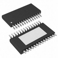
The BUF11705 is available in the TSSOP-28
PowerPAD package for dramatically increased power
dissipation capability. This allows a large number of
channels to be handled safely in one package.
A flow-through pinout has been adopted to allow
simple PCB routing and maintain cost-effectiveness. All
inputs and outputs of the BUF11705 incorporate
internal ESD protection circuits that prevent functional
failures at voltages up to 8 kV (HBM), 2 kV (CDM), and
300 V (MM).
D
D
D
D
D
D
Wide Supply Range: 7 V to 22 V
Gamma Correction Channels: 10
Integrated VCOM Buffer
Excellent Output Current Drive:
− Gamma Channels:
> 30 mA at 0.5 V Swing to Rails(1)
− VCOM:
> 100 mA typ at 2 V Swing to Rails(1)
Large Capacitive Load Drive Capability
Rail-to-Rail Output
PowerPAD Package
Low-Power/Channel: < 500 µA
High ESD Rating: 8 kV HBM, 2 kV CDM,
300 V MM
Specified for −25°C to +85°C
(1) See Typical Characteristic curves for details.
V DD
So urce Driver
BUF117 05
Gamma 1
Gamma 2
Gamma 3
Gamma (n − 2)
Gamma (n − 1)
Gamma (n )
V COM
Please be aware that an important notice concerning availability, standard warranty, and use in critical applications of Texas Instruments
semiconductor products and disclaimers thereto appears at the end of this data sheet.
PowerPAD is a trademark of Texas Instruments. All other trademarks are the property of their respective owners.
Copyright 2005−2007, Texas Instruments Incorporated
��������� �
�
��
�������� �� ������� �� �
����������� ����� ��������
���
��� �� �����
�������� ��� ��� ����� �
����� ����������� �������� ���������
���������� ���������! ���� ��� ����������� ������� ������! �
��� �����������
www.ti.com
�"�#$$%&'
www.ti.com
SBOS349A − DECEMBER 2005 − REVISED DECEMBER 2007
This integrated circuit can be damaged by ESD. Texas Instruments recommends that all integrated circuits be handled with appropriate
precautions. Failure to observe proper handling and installation procedures can cause damage.
ESD damage can range from subtle performance degradation to complete device failure. Precision integrated circuits may be more susceptible to
damage because very small parametric changes could cause the device not to meet its published specifications.
ABSOLUTE MAXIMUM RATINGS(1)
Over operating free-air temperature range unless otherwise noted.
PARAMETERS
Supply voltage, VDD(2)
Input voltage range, VI
BUF11705
UNIT
24
V
Continuous total power dissipation
±VDD
See dissipation rating table
Operating free-air temperature range, TA
−25 to +85
°C
Maximum junction temperature, TJ
+125
°C
Storage temperature range, TSTG
−65 to +150
°C
+260
°C
Human body model (HBM)
8
kV
Charged-device model (CDM)
2
kV
Lead temperature 1.6mm (1/16 inch) from case for 10s
ESD rating:
Machine model (MM)
300
V
(1) Stresses beyond those listed under absolute maximum ratings may cause permanent damage to the device. These are stress ratings only, and
functional operation of the device at these or any other conditions beyond those indicated under recommended operating conditions is not
implied. Exposure to absolute-maximum-rated conditions for extended periods may affect device reliability.
(2) All voltage values are with respect to GND.
ORDERING INFORMATION(1)
PRODUCT
PACKAGE-LEAD
BUF11705
TSSOP-28
PACKAGE MARKING
BUF11705
(1) For the most current package and ordering information, see the Package Option Addendum located at the end of this data sheet or see the
TI website at www.ti.com.
DISSIPATION RATING TABLE
PACKAGE TYPE
PACKAGE
DESIGNATOR
θJC(1)
(°C/W)
TSSOP-28
PWP (28)
0.72
(1) PowerPAD attached to PCB, 0 lfm airflow, and 76mm x 76mm copper area.
qJA(1)
(°C/W)
TA ≤ 25°C
POWER RATING
27.9
3.58 W
RECOMMENDED OPERATING CONDITIONS
MIN
Supply voltage, VDD
Operating free-air temperature, TA
2
NOM
MAX
UNIT
7
22
V
−25
+85
°C
�"�#$$%&'
www.ti.com
SBOS349A − DECEMBER 2005 − REVISED DECEMBER 2007
ELECTRICAL CHARACTERISTICS: BUF11705
Over operating free-air temperature range, VDD = 18 V, TA = +25°C, unless otherwise noted.
PARAMETER
TEST CONDITIONS
Gamma buffers
VIO
Input offset voltage
TA
+25°C
MIN
VCOM
+25°C
−1
Full range(1)
IIB
Input bias current
VI = VDD/2
PSRR
Power-Supply Rejection Ratio
VDD = 4.5 V to 22 V
Buffer gain
VI = 5 V
3dB bandwidth
SR
Slew rate
Crosstalk
IDD
Supply current
ALL
30
VOH1-5
62
Full range(1)
60
VOH6-10
VOL1-5
High-level output
voltage
V/V
+25°C
1
0.6
MHz
CL = 100 pF, RL = 2 kΩ
VIN = 2 V to 16 V
+25°C
1.6
4.6
V/µs
VIPP = 6 V, f = 1 kHz
+25°C
85
dB
25°C
5
VO = VDD/2
No Load
Full range
Low-level output
voltage
VOL6-10
Buffers 1-10 sinking
Buffers 1-10 sourcing
IO = −1 mA to −10 mA
VIN = 17 V
VOHCOM
VOLCOM
Buffers 6-10
High-level output
voltage
VCOM buffer
Low-level output
voltage
VCOM buffer
GND
1
IO = 1 mA to 100 mA,
VIN = 2 V
VIN = 18 V
ISOURCE = 10 mA
VIN = 17 V
ISINK = 10 mA
VIN = 17 V
ISOURCE = 10 mA
VIN = 1 V
ISINK = 10 mA
VIN = 1 V
ISOURCE = 10 mA
VIN = 0 V
ISINK = 10 mA
VIN = 16 V
ISINK = 100 mA
VIN = 16 V
ISOURCE = 100 mA
VIN = 2 V
ISINK = 100 mA
VIN = 2 V
ISOURCE = 100 mA
+25°C
VDD
VDD − 1
VDD
1
Full range
mA
V
5
5
+25°C
1
Full range
5
5
+25°C
1
Full range
5
mV/mA
5
+25°C
1
Full range
+25°C
9.0
9.0
1
+25°C
+25
C
IO = 1 mA to 10 mA
VIN = 1 V
Buffers 1-5
dB
0.9995
IO = −1 mA to −100 mA
VIN = 16 V
Buffers 6-10
80
+25°C
VCOM buffer sourcing
Buffers 1-5
pA
200
+25°C
VCOM buffer
Load regulation
mV
CL = 100 pF, RL = 2 kΩ
Buffers 6-10
VCOM buffer sinking
30
1
Full range(1)
Buffers 1-5
Common-mode input range
UNIT
20
20
+25°C
BW_3dB
MAX
−1
Full range(1)
VI = 9V
Gamma buffers
VCOM buffer
Gamma buffers
VCOM buffer
TYP
5
5
17.85
17.9
17
V
17.15
+25°C
V
16.85
17
1.0
1.15
+25°C
V
0.85
+25°C
1.0
0
0.15
16
16.15
+25°C
V
V
15.85
16
2
+25°C
2.15
V
1.85
2
(1) Full range is −25°C to +85°C.
3
�"�#$$%&'
www.ti.com
SBOS349A − DECEMBER 2005 − REVISED DECEMBER 2007
EQUIVALENT SCHEMATICS OF INPUTS AND OUTPUTS
INPUT STAGE OF BUFFERS
BUF11705: 1 to 5 and VCOM
OUTPUT STAGE OF ALL BUFFERS
INPUT STAGE OF BUFFERS
BUF11705: 6 to 10
VS
VS
VS
Previous
Stage
Next Stage
Next Stage
Buffer
Input
Buffer
Output
Buffer
Input
Buffer
Output
Next Stage
Next Stage
GND
Previous
Stage
GND
GND
Internal to BUF11705
Internal to BUF11705
PIN CONFIGURATION
BUF11705
VDD
1
28
VDD
NC
2
27
NC
OUT1
3
26
IN1(1)
OUT2
4
25
IN2(1)
OUT3
5
24
IN3(1)
OUT4
6
23
IN4(1)
OUT5
7
22
IN5(1)
OUT6
8
21
IN6(1)
OUT7
9
20
IN7(1)
OUT8
10
19
IN8(1)
OUT9
11
18
IN9(1)
OUT10
12
17
IN10(1)
OUTCOM
13
16
INCOM(1)
GND
14
15
GND
TSSOP−28
PowerPAD
NC = No Internal Connection
(1) Connecting a capacitor to this node is not recommended.
4
Inverting
Input
Buffer
Output
�"�#$$%&'
www.ti.com
SBOS349A − DECEMBER 2005 − REVISED DECEMBER 2007
TYPICAL CHARACTERISTICS
Over operating free-air temperature range, unless otherwise noted.
DC CURVES
INPUT OFFSET VOLTAGE vs INPUT VOLTAGE
INPUT OFFSET VOLTAGE vs INPUT VOLTAGE
20
VS = 18 V
Channels 1−5
15
VOS − Input Offset Voltage − mV
VOS − Input Offset Voltage − mV
20
10
5
0
−5
−10
−15
−20
VS = 18 V
Channels 6−10
15
10
5
0
−5
−10
−15
−20
0
3
6
9
12
15
18
0
6
12
15
Figure 1
Figure 2
18
INPUT BIAS CURRENT vs FREE−AIR TEMPERATURE
250
IIB − Input Bias Current − pA
Channels VCOM
VS = 18 V
15
10
5
0
−5
−10
200
150
100
50
−15
0
−20
0
3
6
9
12
15
0
18
10
20
30
40
50
60
70
80 85
TA − Free−Air Temperature − _C
VIN − Input Voltage − V
Figure 3
Figure 4
HIGH−LEVEL OUTPUT VOLTAGE vs
HIGH−LEVEL OUTPUT CURRENT
OUTPUT VOLTAGE vs OUTPUT CURRENT
18
−10_ C
+25_C
VDD = 18 V
Channels 1−5
14
12
+85_ C
10
8
+25_C
6
4
2
−10_ C
0
VOH − High−Level Output Voltage − V
18.0
16
VO − Output Voltage − V
9
VIN − Input Voltage − V
INPUT OFFSET VOLTAGE vs INPUT VOLTAGE
20
VOS − Input Offset Voltage − mV
3
VIN − Input Voltage − V
TA = −10_ C
17.8
TA = +25_ C
17.6
17.4
TA = +85_ C
17.2
VDD = 18 V
Channels 1−5
17.0
0
10
20
30
40
50
60
70
IO − Output Current − mA
Figure 5
80
90
100
0
5
10
IOH
15
20
25
30
35
40
45
50
− High−Level Output Current − mA
Figure 6
5
�"�#$$%&'
www.ti.com
SBOS349A − DECEMBER 2005 − REVISED DECEMBER 2007
TYPICAL CHARACTERISTICS (continued)
Over operating free-air temperature range, unless otherwise noted.
DC CURVES (continued)
BLANK SPACE
OUTPUT VOLTAGE vs OUTPUT CURRENT
LOW−LEVEL OUTPUT VOLTAGE vs
LOW−LEVEL OUTPUT CURRENT (Detailed View)
18
VOL − Low−Level Output Voltage − V
1.0
VO − Output Voltage − V
16
14
12
10
8
−10_ C
6
+25_ C
4
2
+85_C
VSUPPLY = 18 V
Channels 6−10
0
0
10
20
30
40
50
60
70
80
90
Channels 6−10
0.9
0.8
0.7
+85_C
0.6
0.5
0.4
0.3
+25_ C
0.2
−10_ C
0.1
0
100
0
10
I O − Output Current − mA
20
30
40
50
IOL − Low−Level Output Current − mA
Figure 7
Figure 8
OUTPUT VOLTAGE vs OUTPUT CURRENT
SUPPLY CURRENT vs SUPPLY VOLTAGE
18
6
5
14
Supply Current − mA
VO − Output Voltage − V
16
12
VSUPPLY = 18 V
VCOM Buffer
10
+85_ C
+25_C
−10_C
8
6
4
4
3
2
1
2
0
0
0
25
50
75
100 125
150 175 200 225 250
0
2
4
6
8
I O − Output Current − mA
Figure 9
12
14
16
18
20
Figure 10
INPUT BIAS CURRENT vs INPUT VOLTAGE
SUPPLY CURRENT vs FREE−AIR TEMPERATURE
6
5
VS = 18 V
4
5
IB − Input Bias Current − pA
I Q − Supply Current − mA
10
Supply Voltage − V
4
3
2
1
3
2
1
0
−1
−2
−3
−4
−5
0
−50
−25
0
25
50
75
TA − Free−Air Temperature − _C
Figure 11
6
100
125
0
2
4
6
8
10
12
14
VIN − Input Voltage − V
Figure 12
16
18
20
�"�#$$%&'
www.ti.com
SBOS349A − DECEMBER 2005 − REVISED DECEMBER 2007
TYPICAL CHARACTERISTICS (continued)
Over operating free-air temperature range, unless otherwise noted.
POWER−SUPPLY REJECTION RATIO vs FREQUENCY
VDD = 10 V
RL = 2 k
CL = 100 pF
80
70
60
50
Gamma Channels
40
VCOM Buffer
30
20
10
0
10
100
1k
10 k
100 k
f − Frequency − Hz
Figure 13
1M
10 M
CMRR − Common−Mode Rejection Ratio − dB
PSRR − Power−Supply Rejection Ratio − dB
AC CURVES
CROSSTALK vs FREQUENCY
0
VSUPPLY = 10 V
VIN = 1 VPP
20
40
60
80
100
120
140
10
100
1k
10 k
100 k
1M
f − Frequency − Hz
Figure 14
7
�"�#$$%&'
www.ti.com
SBOS349A − DECEMBER 2005 − REVISED DECEMBER 2007
TYPICAL CHARACTERISTICS (continued)
Over operating free-air temperature range, unless otherwise noted.
SMALL- AND LARGE-SIGNAL WAVEFORM CURVES
SMALL−SIGNAL WAVEFORM
50 mV/div
50 mV/div
SMALL−SIGNAL WAVEFORM
RLOAD = 2 kΩ
CLOAD = 100 pF
Channels 1−5
t − Time − 500 ns/div
RLOAD = 2 kΩ
CLOAD = 100 pF
Channels 6−10
t − Time − 500 ns/div
Figure 16
Figure 15
SMALL−SIGNAL WAVEFORMVCOM BUFFER
LARGE−SIGNAL WAVEFORM
RLOAD = 2 kΩ
CLOAD = 100 pF
VCOM Buffer
3 V/div
50 mV/div
RLOAD = 2 kΩ
CLOAD = 100 pF
VDD = 15 V
t − Time − 500 ns/div
Channels 1−5
t − Time − 4 µs/div
Figure 17
Figure 18
LARGE−SIGNAL WAVEFORMVCOM BUFFER
LARGE−SIGNAL WAVEFORM
RLOAD = 2 kΩ
C LOAD = 100 pF
VCOM Buffer
VDD = 15 V
3 V/div
3 V/div
RLOAD = 2 kΩ
CLOAD = 100 pF
VDD = 15 V
Channels 6−10
8
t − Time − 4 µs/div
t − Time − 4 µs/div
Figure 19
Figure 20
�"�#$$%&'
www.ti.com
SBOS349A − DECEMBER 2005 − REVISED DECEMBER 2007
correction resistor ladder. The low output impedance of
the BUF11705 forces the external gamma correction
voltage on the respective reference node of the LCD
source driver. Figure 21 shows an example of the
BUF11705 in a typical block diagram driving an LCD
source driver with 10-channel gamma correction
reference inputs.
APPLICATION INFORMATION
The requirements on the number of gamma correction
channels vary greatly from panel to panel. Therefore,
the BUF11705 series of gamma correction buffers offer
different channel combinations using 10 gamma
channels plus one VCOM channel. The VCOM channel
can be used to drive the VCOM node on the LCD panel.
Gamma correction voltages are often generated using
a simple resistor ladder, as shown in Figure 21. The
BUF11705 buffers the various nodes on the gamma
VDD
Source Driver
BUF11705
RS(1)
Gamma 1
(2)
(1)
Gamma 2
(2)
(1)
Gamma 3
(2)
(1)
Gamma 8
(2)
(1)
Gamma 9
(2)
(1)
Gamma 10
(2)
VCOM
(1) Optional resistor increases stability.
(2) Optional capacitor.
Figure 21. LCD Source Driver Typical Block Diagram
9
�"�#$$%&'
www.ti.com
SBOS349A − DECEMBER 2005 − REVISED DECEMBER 2007
ESD RATINGS
The BUF11705 has excellent ESD performance: 8 kV
HBM; 2 kV CDM; and 300 V MM. These ESD ratings
allow for increased manufacturability, fewer production
failures, and higher reliability.
INPUT VOLTAGE RANGE GAMMA BUFFERS
Figure 22 shows a typical gamma correction curve with
10 gamma correction reference points (GMA1 through
GMA10). As can be seen from this curve, the voltage
requirements for each buffer vary greatly. The swing
capability of the input stages of the various buffers is
carefully matched to the application. Buffers 1 through
5 have input stages that include VDD, but will only swing
within 1 V to GND. Buffers 1 through 5 have only a single
NMOS input stage. Buffers 6 through 10 have only a
single PMOS input stage. The input range of the PMOS
input stage includes GND.
VDD1
GMA1
VDD (typically, VCC − 100 mV at 10 mA). The ability of
buffers 1 through 5 to swing to GND is limited. Buffers
6 through 10 swing closer to GND than VDD. Buffers 6
through 10 are designed to swing very close to GND;
typically, GND + 100 mV at a 10 mA load current. See
the Typical Characteristics for more details. This
approach significantly reduces the silicon area and
overall cost of the whole solution. However, due to this
architecture, the correct buffer must be connected to
the correct gamma correction voltage. Connect buffer
1 to the gamma voltage closest to VDD, and buffers 2
through 5 to the sequentially voltages. Buffer 10 should
be connected to the gamma correction voltage closest
to GND (or the negative rail), and buffers 9 through 6 to
the sequentially higher voltages.
COMMON BUFFER (VCOM)
The common buffer output of the BUF11705 has a
greater output drive capability than the gamma buffers
in order to meet the heavier current demands of driving
the common node of the LCD panel. The common
buffer output was also designed to drive heavier
capacitive loads. Excellent output swing is possible with
high currents ( > 100 mA), as shown in Figure 23.
GMA2
GMA3
GMA4
GMA5
OUTPUT VOLTAGE vs OUTPUT CURRENT
GMA6
GMA10
VSS1
0
10
20
30
40
Input Data (Hex)
Figure 22. Gamma Correction Curve
Output Voltage − V
GMA7
GMA8
GMA9
18
17
16
15
14
13
12
11
VDD = 18 V
TA = 25_ C
7
6
5
4
3
2
1
0
0
OUTPUT VOLTAGE SWING GAMMA BUFFERS
The output stages have been designed to match the
characteristic of the input stage. This means that the
output stage of buffers 1 through 5 swing very close to
10
25
50
75
100 125 150 175 200 225 250
Output Current − mA
Figure 23. VCOM Output Drive Capability
�"�#$$%&'
www.ti.com
SBOS349A − DECEMBER 2005 − REVISED DECEMBER 2007
CAPACITIVE LOAD DRIVE
APPLICATIONS WITH >10 GAMMA CHANNELS
The BUF11705 has been designed to sink/source large
dc currents. Its output stage has been designed to
deliver output current transients with little disturbance
of the output voltage. However, there are times when
very fast current pulses are required. Therefore, in LCD
source driver buffer applications, it is quite normal for
capacitors to be placed at the outputs of the reference
buffers. These capacitors improve the transient load
regulation and will typically have values of 100pF or
more. The BUF11705 gamma buffers were designed to
drive capacitances in excess of 100 pF. The output is
able to swing within 150 mV of the rails on
10 mA of output current, as shown in Figure 24.
When a greater number of gamma correction channels
are required, two or more BUF11705 devices can be
used in parallel, as shown in Figure 25. This capability
provides a cost-effective way of creating more reference voltages over the use of quad-channel op amps or
buffers. The suggested configuration in Figure 25
simplifies layout. The various different channel versions
provide a high degree of flexibility and also minimize
total cost and space.
OUTPUT VOLTAGE vs OUTPUT CURRENT
BUF11705
OUT1
GMA1
OUT2
2
OUT3
3
OUT4
4
OUT5
5
OUT6
6
OUT7
7
OUT8
8
OUT9
9
18.0
VDD = 18 V
TA = 25_C
17.8
Channels 1−5
Output Voltage − V
17.6
17.4
17.2
17.0
1.0
0.8
0.6
0.4
OUT10
GMA10
OUT11
GMA11
OUT12
12
OUT13
13
OUT14
14
OUT15
15
OUT16
16
OUT17
17
OUT18
18
OUT19
19
OUT20
GMA20
Channels 6−10
0.2
0
0
5
10
15
20
25
30
35
40
45
Output Current − mA
Figure 24. Gamma Buffer Drive Capability
50
BUF11705
Figure 25. Creating > 10 Gamma Voltage
Channels
11
�"�#$$%&'
www.ti.com
SBOS349A − DECEMBER 2005 − REVISED DECEMBER 2007
COMPLETE LCD SOLUTION FROM TI
In addition to the BUF11705 line of gamma correction
buffers, TI offers a complete set of ICs for the LCD panel
market, including various power-supply solutions, and
audio power solutions. Figure 26 shows the total IC
solution from TI.
Reference
VCOM
Gamma Correction
BUF11705
2.7 V to 5 V
TPS651xx
LCD
Supply
15 V
26 V
−14 V
3.3 V
TPA300x
Audio
Speaker
Driver
n
Logic and
Timing
Controller
Gate Driver
Source Driver
High−Resolution
TFT−LCS Panel
Figure 26. TI LCD Solution
12
n
�"�#$$%&'
www.ti.com
SBOS349A − DECEMBER 2005 − REVISED DECEMBER 2007
The BUF11705 is available in the thermally-enhanced
PowerPAD package. This package is constructed using
a downset leadframe upon which the die is mounted, as
shown in Figure 27(a) and (b). This arrangement
results in the lead frame being exposed as a thermal
pad on the underside of the package; see Figure 27(c).
Due to this thermal pad having direct thermal contact
with the die, excellent thermal performance is achieved
by providing a good thermal path away from the thermal
pad.
The PowerPAD package allows for both assembly and
thermal management in one manufacturing operation.
During the surface-mount solder operation (when the
leads are being soldered), the thermal pad must be
soldered to a copper area underneath the package.
Through the use of thermal paths within this copper
area, heat can be conducted away from the package
into either a ground plane or other heat-dissipating
device. Soldering the PowerPAD to the PCB is
always required, even with applications that have
low power dissipation. This provides the necessary
thermal and mechanical connection between the lead
frame die pad and the PCB.
The PowerPAD must be connected to the most
negative supply voltage of the device.
1. Prepare the PCB with a top-side etch pattern. There
should be etching for the leads as well as etch for the
thermal pad.
2. Place recommended holes in the area of the thermal
pad. Ideal thermal land size and thermal via patterns
can be seen in technical brief, SLMA002 PowerPAD
Thermally-Enhanced Package, available for download at www.ti.com. These holes should be 13 mils
(0.33 mm) in diameter. Keep them small, so that
solder wicking through the holes is not a problem
during reflow.
DIE
Side View (a)
3. Additional vias may be placed anywhere along the
thermal plane outside of the thermal pad area. This
helps dissipate the heat generated by the
BUF11705 IC. These additional vias may be larger
than the 13-mil diameter vias directly under the
thermal pad. They can be larger because they are
not in the thermal pad area to be soldered; so that,
wicking is not a problem.
4. Connect all holes to the internal ground plane.
5. When connecting these holes to the ground plane,
do not use the typical web or spoke via connection
methodology. Web connections have a high thermal
resistance connection that is useful for slowing the
heat transfer during soldering operations. Web
connections make the soldering of vias easier. In
this application, however, low thermal resistance is
desired for the most efficient heat transfer.
Therefore, the holes under the BUF11705
PowerPAD package should make their connection
to the internal ground plane with a complete
connection around the entire circumference of the
plated-through hole.
6. The top-side solder mask should leave the terminals
of the package and the thermal pad area with its ten
holes exposed. The bottom-side solder mask
should cover the holes of the thermal pad area. This
prevents solder from being pulled away from the
thermal pad area during the reflow process.
7. Apply solder paste to the exposed thermal pad area
and all of the IC terminals.
8. With these preparatory steps in place, the
BUF11705 IC is simply placed in position and run
through the solder reflow operation as any standard
surface-mount component. This preparation results
in a properly installed part.
Thermal
Pad
GENERAL PowerPAD DESIGN
CONSIDERATIONS
DIE
End View (b)
Bottom View (c)
The thermal pad is electrically isolated from all terminals in the package.
Figure 27. Views of Thermally-Enhanced DGN Package
13
�"�#$$%&'
www.ti.com
SBOS349A − DECEMBER 2005 − REVISED DECEMBER 2007
For a given qJA, the maximum power dissipation is
shown in Figure 28, and is calculated by the following
formula:
T MAX * T A
PD +
q JA
ǒ
Where:
PD = maximum power dissipation (W)
TMAX = absolute maximum junction temperature (125°C)
Ǔ
TA = free-ambient air temperature (°C)
qJA = qJC + qCA
qJC = thermal coefficient from junction to case (°C/W)
qCA = thermal coefficient from case-to-ambient air (°C/W)
8
TSSOP−28
Maximum Power Dissipation − W
7
6
5
4
3
2
1
0
Dissipation with PowerPAD
soldered down.
−40
−20
0
20
40
60
80
100
TA −Free−Air Temperature −_C
Figure 28. Views of Thermally-Enhanced DGN Package
14
�PACKAGE OPTION ADDENDUM
www.ti.com
10-Dec-2020
PACKAGING INFORMATION
Orderable Device
Status
(1)
Package Type Package Pins Package
Drawing
Qty
Eco Plan
(2)
Lead finish/
Ball material
MSL Peak Temp
Op Temp (°C)
Device Marking
(3)
(4/5)
(6)
BUF11705AIPWPR
NRND
HTSSOP
PWP
28
2000
RoHS & Green
NIPDAU
Level-2-260C-1 YEAR
-25 to 85
BUF11705
(1)
The marketing status values are defined as follows:
ACTIVE: Product device recommended for new designs.
LIFEBUY: TI has announced that the device will be discontinued, and a lifetime-buy period is in effect.
NRND: Not recommended for new designs. Device is in production to support existing customers, but TI does not recommend using this part in a new design.
PREVIEW: Device has been announced but is not in production. Samples may or may not be available.
OBSOLETE: TI has discontinued the production of the device.
(2)
RoHS: TI defines "RoHS" to mean semiconductor products that are compliant with the current EU RoHS requirements for all 10 RoHS substances, including the requirement that RoHS substance
do not exceed 0.1% by weight in homogeneous materials. Where designed to be soldered at high temperatures, "RoHS" products are suitable for use in specified lead-free processes. TI may
reference these types of products as "Pb-Free".
RoHS Exempt: TI defines "RoHS Exempt" to mean products that contain lead but are compliant with EU RoHS pursuant to a specific EU RoHS exemption.
Green: TI defines "Green" to mean the content of Chlorine (Cl) and Bromine (Br) based flame retardants meet JS709B low halogen requirements of


 工商网监
湘ICP备2023018690号
工商网监
湘ICP备2023018690号
