SN74ALVC164245-EP
16-BIT 2.5-V TO 3.3-V/3.3-V TO 5-V LEVEL-SHIFTING TRANSCEIVER
WITH 3-STATE OUTPUTS
www.ti.com
SCAS774A – JUNE 2004 – REVISED SEPTEMBER 2005
FEATURES
•
•
•
•
•
•
•
•
•
(1)
Controlled Baseline
– One Assembly/Test Site, One Fabrication
Site
Enhanced Diminishing Manufacturing
Sources (DMS) Support
Enhanced Product-Change Notification
Qualification Pedigree(1)
Member of the Texas Instruments Widebus™
Family
Max tpd of 5.8 ns at 3.3 V
±24-mA Output Drive at 3.3 V
Control Inputs VIH/VIL Levels Are Referenced
to VCCA Voltage
Latch-Up Performance Exceeds 250 mA Per
JESD 17
Component qualification in accordance with JEDEC and
industry standards to ensure reliable operation over an
extended temperature range. This includes, but is not limited
to, Highly Accelerated Stress Test (HAST) or biased 85/85,
temperature cycle, autoclave or unbiased HAST,
electromigration, bond intermetallic life, and mold compound
life. Such qualification testing should not be viewed as
justifying use of this component beyond specified
performance and environmental limits.
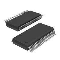
DGG OR DL PACKAGE
(TOP VIEW)
1DIR
1B1
1B2
GND
1B3
1B4
(3.3 V, 5 V) VCCB
1B5
1B6
GND
1B7
1B8
2B1
2B2
GND
2B3
2B4
(3.3 V, 5 V) VCCB
2B5
2B6
GND
2B7
2B8
2DIR
1
48
2
47
3
46
4
45
5
44
6
43
7
42
8
41
9
40
10
39
11
38
12
37
13
36
14
35
15
34
16
33
17
32
18
31
19
30
20
29
21
28
22
27
23
26
24
25
1OE
1A1
1A2
GND
1A3
1A4
VCCA (2.5 V, 3.3 V)
1A5
1A6
GND
1A7
1A8
2A1
2A2
GND
2A3
2A4
VCCA (2.5 V, 3.3 V)
2A5
2A6
GND
2A7
2A8
2OE
DESCRIPTION/ORDERING INFORMATION
This 16-bit (dual-octal) noninverting bus transceiver contains two separate supply rails. B port has VCCB, which is
set to operate at 3.3 V and 5 V. A port has VCCA, which is set to operate at 2.5 V and 3.3 V. This allows for
translation from a 2.5-V to a 3.3-V environment, and vice versa, or from a 3.3-V to a 5-V environment, and vice
versa.
The SN74ALVC164245 is designed for asynchronous communication between data buses. The control circuitry
(1DIR, 2DIR, 1OE, and 2OE) is powered by VCCA.
To ensure the high-impedance state during power up or power down, the output-enable (OE) input should be tied
to VCC through a pullup resistor; the minimum value of the resistor is determined by the current-sinking capability
of the driver.
ORDERING INFORMATION
PACKAGE (1)
TA
–40°C to 85°C
(1)
TOP-SIDE MARKING
Reel of 1000
CALVC164245IDLREP
ALVC164245
TSSOP – DGG
Reel of 2000
CALVC164245IDGGREP
ALVC164245
VFBGA – GQL
VFBGA – ZQL (Pb-free)
–55°C to 125°C
ORDERABLE PART NUMBER
SSOP – DL
TSSOP – DGG
Reel of 1000
Reel of 2000
CALVC164245IGQLREP
CALVC164245IZQLREP
CALVC164245MDGGREP
VC4245EP
C164245MEP
Package drawings, standard packing quantities, thermal data, symbolization, and PCB design guidelines are available at
www.ti.com/sc/package.
Please be aware that an important notice concerning availability, standard warranty, and use in critical applications of Texas
Instruments semiconductor products and disclaimers thereto appears at the end of this data sheet.
Widebus is a trademark of Texas Instruments.
PRODUCTION DATA information is current as of publication date.
Products conform to specifications per the terms of the Texas
Instruments standard warranty. Production processing does not
necessarily include testing of all parameters.
Copyright © 2004–2005, Texas Instruments Incorporated
�SN74ALVC164245-EP
16-BIT 2.5-V TO 3.3-V/3.3-V TO 5-V LEVEL-SHIFTING TRANSCEIVER
WITH 3-STATE OUTPUTS
www.ti.com
SCAS774A – JUNE 2004 – REVISED SEPTEMBER 2005
GQL OR ZQL PACKAGE
(TOP VIEW)
1
2
3
4
5
TERMINAL ASSIGNMENTS (1)
1
6
2
3
5
6
A
1DIR
NC
NC
NC
NC
1OE
A
B
1B2
1B1
GND
GND
1A1
1A2
B
C
1B4
1B3
VCCB
VCCA
1A3
1A4
D
1B6
1B5
GND
GND
1A5
1A6
E
1B8
1B7
1A7
1A8
F
2B1
2B2
2A2
2A1
G
2B3
2B4
GND
GND
2A4
2A3
2A5
C
D
E
F
H
2B5
2B6
VCCB
VCCA
2A6
G
J
2B7
2B8
GND
GND
2A8
2A7
H
K
2DIR
NC
NC
NC
NC
2OE
J
K
(1)
NC – No internal connection
FUNCTION TABLE
(EACH 8-BIT SECTION)
INPUTS
OE
2
4
DIR
OPERATION
L
L
B data to A bus
L
H
A data to B bus
H
X
Isolation
�SN74ALVC164245-EP
16-BIT 2.5-V TO 3.3-V/3.3-V TO 5-V LEVEL-SHIFTING TRANSCEIVER
WITH 3-STATE OUTPUTS
www.ti.com
SCAS774A – JUNE 2004 – REVISED SEPTEMBER 2005
LOGIC DIAGRAM (POSITIVE LOGIC)
1DIR
1
2DIR
48
1A1
25
1OE
47
2A1
2
24
2OE
36
13
1B1
2B1
To Seven Other Channels
To Seven Other Channels
Pin numbers shown are for the DGG and DL packages.
Absolute Maximum Ratings (1)
over operating free-air temperature range for VCCB at 5 V and VCCA at 3.3 V (unless otherwise noted)
VCCA
VCCB
Supply voltage range
Except I/O ports (2)
VI
Input voltage range
MIN
MAX
–0.5
4.6
–0.5
6
–0.5
6
A (3)
–0.5 VCCA + 0.5
I/O port B (2)
–0.5 VCCB + 0.5
I/O port
UNIT
V
V
IIK
Input clamp current
VI < 0
–50
mA
IOK
Output clamp current
VO < 0
–50
mA
IO
Continuous output current
±50
mA
±100
mA
Continuous current through each VCC or GND
θJA
Tstg
(1)
(2)
(3)
(4)
Package thermal impedance (4)
Storage temperature range
DGG package
70
DL package
63
GQL/ZQL package
42
–65
150
°C/W
°C
Stresses beyond those listed under "absolute maximum ratings" may cause permanent damage to the device. These are stress ratings
only, and functional operation of the device at these or any other conditions beyond those indicated under "recommended operating
conditions" is not implied. Exposure to absolute-maximum-rated conditions for extended periods may affect device reliability.
This value is limited to 6 V maximum.
This value is limited to 4.6 V maximum.
The package thermal impedance is calculated in accordance with JESD 51-7.
3
�SN74ALVC164245-EP
16-BIT 2.5-V TO 3.3-V/3.3-V TO 5-V LEVEL-SHIFTING TRANSCEIVER
WITH 3-STATE OUTPUTS
www.ti.com
SCAS774A – JUNE 2004 – REVISED SEPTEMBER 2005
Recommended Operating Conditions (1)
for VCCB at 3.3 V and 5 V
MIN
MAX
VCCB
Supply voltage
3
5.5
VIH
High-level input voltage
2
VIL
Low-level input voltage
VIB
Input voltage
0
VCCB
VOB
Output voltage
0
VCCB
V
IOH
High-level output current
–24
mA
IOL
Low-level output current
24
mA
∆t/∆v
Input transition rise or fall rate
10
ns/V
TA
(1)
Operating free-air temperature
UNIT
V
V
VCCB = 3 V to 3.6 V
0.7
VCCB = 4.5 V to 5.5 V
0.8
CALVC16245I
–40
85
CALVC16245M
–55
125
V
V
°C
All unused inputs of the device must be held at VCC or GND to ensure proper device operation. Refer to the TI application report,
Implications of Slow or Floating CMOS Inputs, literature number SCBA004.
Recommended Operating Conditions (1)
for VCCA at 2.5 V and 3.3 V
VCCA
Supply voltage
VIH
High-level input voltage
VIL
Low-level input voltage
VIA
Input voltage
VOA
Output voltage
IOH
High-level output current
IOL
Low-level output current
∆t/∆v
Input transition rise or fall rate
TA
(1)
4
Operating free-air temperature
VCCA = 2.3 V to 2.7 V
VCCA = 3 V to 3.6 V
MIN
MAX
2.3
3.6
1.7
UNIT
V
V
2
VCCA = 2.3 V to 2.7 V
0.7
VCCA = 3 V to 3.6 V
0.8
V
0
VCCA
V
0
VCCA
V
VCCA = 2.3 V
–18
VCCA = 3 V
–24
VCCA = 2.3 V
18
VCCA = 3 V
24
10
CALVC16245I
–40
85
CALVC16245M
–55
125
All unused inputs of the device must be held at VCC or GND to ensure proper device operation. Refer to the TI application report,
Implications of Slow or Floating CMOS Inputs, literature number SCBA004.
mA
mA
ns/V
°C
�SN74ALVC164245-EP
16-BIT 2.5-V TO 3.3-V/3.3-V TO 5-V LEVEL-SHIFTING TRANSCEIVER
WITH 3-STATE OUTPUTS
www.ti.com
SCAS774A – JUNE 2004 – REVISED SEPTEMBER 2005
Electrical Characteristics
over recommended operating free-air temperature range for VCCA = 2.7 V to 3.6 V and VCCB = 4.5 V to 5.5 V
(unless otherwise noted)
PARAMETER
TEST CONDITIONS
IOH = –100 µA
B to A
IOH = –12 mA
IOH = –24 mA
VOH
VCCA
2.7 V to
3.6 V
MIN TYP (1)
CALVC164245M
MAX
MIN TYP (1) MAX
VCC – 0.2
2.7 V
2.2
2.2
3V
2.4
2.4
3V
2
2
4.5 V
4.3
4.3
5.5 V
5.3
5.3
4.5 V
3.7
3.7
5.5 V
4.7
4.7
A to B
IOL = 24 mA
VOL
CALVC164245I
VCC – 0.2
IOL = 100 µA
B to A
VCCB
V
IOL = 100 µA
2.7 V to
3.6 V
0.2
0.2
IOL = 12 mA
2.7 V
0.4
0.4
IOL = 24 mA
3V
0.55
0.55
IOL = 100 µA
4.5 V to
5.5 V
0.2
0.2
IOL = 24 mA
4.5 V to
5.5 V
0.55
0.55
A to B
UNIT
V
II
Control
inputs
VI = VCCA/VCCB or GND
3.6 V
5.5 V
±5
±5
µA
IOZ (2)
A or B
port
VO = VCCA/VCCB or GND
3.6 V
5.5 V
±10
±10
µA
ICC
VI = VCCA/VCCB or GND,
IO = 0
5.5 V
5.5 V
40
40
µA
∆ICC (3)
One input at VCCA/VCCB – 0.6 V,
Other inputs at VCCA/VCCB or GND
3 V to
3.6 V
4.5 V to
5.5 V
750
750
µA
Ci
Control
inputs
VI = VCCA/VCCB or GND
3.3 V
5V
6.5
6.5
pF
Cio
A or B
port
VO = VCCA/VCCB or GND
3.3 V
3.3 V
8.5
8.5
pF
(1)
(2)
(3)
All typical values are at VCCA = 3.3 V and VCCB = 5 V, TA = 25°C.
For I/O ports, the parameter IOZ includes the input leakage current.
This is the increase in supply current for each input that is at one of the specified TTL voltage levels, rather than at 0 or the associated
VCC.
5
�SN74ALVC164245-EP
16-BIT 2.5-V TO 3.3-V/3.3-V TO 5-V LEVEL-SHIFTING TRANSCEIVER
WITH 3-STATE OUTPUTS
www.ti.com
SCAS774A – JUNE 2004 – REVISED SEPTEMBER 2005
Electrical Characteristics
over recommended operating free-air temperature range for VCCA = 2.3 V to 2.7 V and VCCB = 3 V to 3.6 V
(unless otherwise noted)
PARAMETER
TEST CONDITIONS
CALVC164245I
CALVC164245M
VCCA
VCCB
2.3 V to 2.7 V
3 V to 3.6 V
VCCA – 0.2
VCCA – 0.2
2.3 V
3 V to 3.6 V
1.7
1.7
IOH = –12 mA
2.7 V
3 V to 3.6 V
1.8
1.8
IOL = 100 µA
2.3 V to 2.7 V
3 V to 3.6 V
VCCB – 0.2
VCCB – 0.2
IOL = 18 mA
2.3 V to 2.7 V
3V
2.2
2.2
IOL = 100 µA
2.3 V to 2.7 V
3 V to 3.6 V
0.2
0.2
IOL = 12 mA
2.3 V
3 V to 3.6 V
0.6
0.6
IOL = 100 µA
2.3 V to 2.7 V
3 V to 3.6 V
0.2
0.2
IOL = 18 mA
2.3 V
3V
0.55
0.55
VI = VCCA/VCCB or GND
2.3 V to 2.7 V
3 V to 3.6 V
±5
±5
µA
IOZ (1) A or B
port
VO = VCCA/VCCB or GND
2.3 V to 2.7 V
3 V to 3.6 V
±10
±10
µA
ICC
VI = VCCA/VCCB or GND,
IO = 0
2.3 V to 2.7 V
3 V to 3.6 V
20
40
µA
∆ICC (2)
One input at VCCA/VCCB – 0.6 V,
Other inputs at VCCA/VCCB or GND
2.3 V to 2.7 V
3 V to 3.6 V
750
750
µA
IOH = –100 µA
B to A
VOH
A to B
B to A
VOL
A to B
II
(1)
(2)
6
Control
inputs
IOH = –8 mA
MIN MAX
MIN
MAX
UNIT
V
V
For I/O ports, the parameter IOZ includes the input leakage current.
This is the increase in supply current for each input that is at one of the specified TTL voltage levels, rather than at 0 or the associated
VCC.
�SN74ALVC164245-EP
16-BIT 2.5-V TO 3.3-V/3.3-V TO 5-V LEVEL-SHIFTING TRANSCEIVER
WITH 3-STATE OUTPUTS
www.ti.com
SCAS774A – JUNE 2004 – REVISED SEPTEMBER 2005
Switching Characteristics
over recommended operating free-air temperature range (unless otherwise noted) (see Figure 1 through Figure 4)
CALVC16245I
PARAMETER
FROM
(INPUT)
TO
(OUTPUT)
VCCB = 3.3 V
± 0.3 V
VCCA = 2.5 V
± 0.2 V
MIN
tpd
MAX
VCCB = 5 V ± 0.5 V
VCCA = 3.3 V
± 0.3 V
VCCA = 2.7 V
MIN
MAX
MIN
MAX
A
B
7.6
5.9
1
5.8
B
A
7.6
6.7
1.2
5.8
UNIT
ns
ten
OE
B
11.5
9.3
1
8.9
ns
tdis
OE
B
10.5
9.2
2.1
9.5
ns
ten
OE
A
12.3
10.2
2
9.1
ns
tdis
OE
A
9.3
9
2.9
8.6
ns
Switching Characteristics
over recommended operating free-air temperature range (unless otherwise noted) (see Figure 1 through Figure 4)
CALVC16245M
PARAMETER
VCCB = 3.3 V
± 0.3 V
VCCB = 5 V ± 0.5 V
FROM
(INPUT)
TO
(OUTPUT)
MAX
MIN
MAX
A
B
8.6
6.9
1
6.8
B
A
8.6
7.7
1.2
6.8
VCCA = 2.5 V
± 0.2 V
MIN
tpd
MAX
VCCA = 2.7 V
MIN
VCCA = 3.3 V
± 0.3 V
UNIT
ns
ten
OE
B
12.5
10.3
1
9.9
ns
tdis
OE
B
11.5
10.2
2.1
10.5
ns
ten
OE
A
14.5
11.2
2
10.1
ns
tdis
OE
A
11.3
11
2.9
10.6
ns
Operating Characteristics
TA = 25°C
PARAMETER
TEST CONDITIONS
Outputs enabled (B)
Cpd
Power dissipation capacitance
Outputs disabled (B)
Outputs enabled (A)
Outputs disabled (A)
CL = 50 pF,
f = 10 MHz
CL = 50 pF,
f = 10 MHz
VCCB = 3.3 V
VCCB = 5 V
VCCA = 2.5 V
VCCA = 3.3 V
TYP
TYP
55
56
27
6
118
56
58
6
UNIT
pF
7
�SN74ALVC164245-EP
16-BIT 2.5-V TO 3.3-V/3.3-V TO 5-V LEVEL-SHIFTING TRANSCEIVER
WITH 3-STATE OUTPUTS
www.ti.com
SCAS774A – JUNE 2004 – REVISED SEPTEMBER 2005
Power-Up Considerations (1)
TI level-translation devices offer an opportunity for successful mixed-voltage signal design. A proper power-up
sequence always should be followed to avoid excessive supply current, bus contention, oscillations, or other
anomalies caused by improperly biased device pins. To guard against such power-up problems, take these
precautions:
1. Connect ground before any supply voltage is applied.
2. Power up the control side of the device (VCCA for all four of these devices).
3. Tie OE to VCCA with a pullup resistor so that it ramps with VCCA.
4. Depending on the direction of the data path, DIR can be high or low. If DIR high is needed (A data to B bus),
ramp it with VCCA. Otherwise, keep DIR low.
(1)
8
Refer to the TI application report, Texas Instruments Voltage-Level-Translation Devices, literature number SCEA021.
�SN74ALVC164245-EP
16-BIT 2.5-V TO 3.3-V/3.3-V TO 5-V LEVEL-SHIFTING TRANSCEIVER
WITH 3-STATE OUTPUTS
www.ti.com
SCAS774A – JUNE 2004 – REVISED SEPTEMBER 2005
PARAMETER MEASUREMENT INFORMATION
VCCA = 2.5 V ± 0.2 V to VCCB = 3.3 V ± 0.3 V
VCCB = 6 V
500 Ω
From Output
Under Test
S1
Open
GND
CL = 30 pF
(see Note A)
500 Ω
TEST
S1
tpd
tPLZ/tPZL
tPHZ/tPZH
Open
VCCB = 6 V
GND
LOAD CIRCUIT
VCCA
Output
Control
(low-level
enabling)
VCCA/2
0V
tPZL
VCCA
Input
VCCA/2
VCCA/2
0V
tPLH
tPHL
VOHB
Output
1.5 V
1.5 V
VOLB
VOLTAGE WAVEFORMS
PROPAGATION DELAY TIMES
tPLZ
VCCB
Output
Waveform 1
S1 at 6 V
(see Note B)
Output
Waveform 2
S1 at GND
(see Note B)
VCCA/2
1.5 V
VOL + 0.3 V
VOLB
tPZH
tPHZ
1.5 V
VOH − 0.3 V
VOHB
0V
VOLTAGE WAVEFORMS
ENABLE AND DISABLE TIMES
NOTES: A. CL includes probe and jig capacitance.
B. Waveform 1 is for an output with internal conditions such that the output is low, except when disabled by the output control.
Waveform 2 is for an output with internal conditions such that the output is high, except when disabled by the output control.
C. All input pulses are supplied by generators having the following characteristics: PRR≤ 10 MHz, ZO = 50 Ω, tr≤ 2 ns, tf≤ 2 ns.
D. The outputs are measured one at a time, with one transition per measurement.
E. tPLZ and tPHZ are the same as tdis.
F. tPZL and tPZH are the same as ten.
G. tPLH and tPHL are the same as tpd.
Figure 1. Load Circuit and Voltage Waveforms
9
�SN74ALVC164245-EP
16-BIT 2.5-V TO 3.3-V/3.3-V TO 5-V LEVEL-SHIFTING TRANSCEIVER
WITH 3-STATE OUTPUTS
www.ti.com
SCAS774A – JUNE 2004 – REVISED SEPTEMBER 2005
PARAMETER MEASUREMENT INFORMATION
VCCB = 3.3 V ± 0.3 V to VCCA = 2.5 V ± 0.2 V
2 × VCCA
500 Ω
From Output
Under Test
S1
Open
TEST
tpd
tPLZ/tPZL
tPHZ/tPZH
GND
CL = 30 pF
(see Note A)
500 Ω
S1
Open
2 × VCCA
GND
LOAD CIRCUIT
Output
Control
(low-level
enabling)
2.7 V
1.5 V
0V
tPZL
2.7 V
Input
1.5 V
1.5 V
0V
tPLH
VCCA/2
VCCA/2
VOLA
VOLTAGE WAVEFORMS
PROPAGATION DELAY TIMES
tPLZ
VCCA
VCCA/2
tPZH
VOHA
Output
Output
Waveform 1
S1 at 2 × VCCA
(see Note B)
tPHL
1.5 V
Output
Waveform 2
S1 at GND
(see Note B)
VOL + 0.15 V
VOLA
tPHZ
VCCA/2
VOHA
VOH − 0.15 V
0V
VOLTAGE WAVEFORMS
ENABLE AND DISABLE TIMES
NOTES: A. CL includes probe and jig capacitance.
B. Waveform 1 is for an output with internal conditions such that the output is low, except when disabled by the output control.
Waveform 2 is for an output with internal conditions such that the output is high, except when disabled by the output control.
C. All input pulses are supplied by generators having the following characteristics: PRR ≤ 10 MHz, ZO = 50 Ω, tr ≤ 2 ns, tf ≤ 2 ns.
D. The outputs are measured one at a time, with one transition per measurement.
E. tPLZ and tPHZ are the same as tdis.
F. tPZL and tPZH are the same as ten.
G. tPLH and tPHL are the same as tpd.
Figure 2. Load Circuit and Voltage Waveforms
10
�SN74ALVC164245-EP
16-BIT 2.5-V TO 3.3-V/3.3-V TO 5-V LEVEL-SHIFTING TRANSCEIVER
WITH 3-STATE OUTPUTS
www.ti.com
SCAS774A – JUNE 2004 – REVISED SEPTEMBER 2005
PARAMETER MEASUREMENT INFORMATION
VCCA = 3.3 V ± 0.3 V to VCCB = 5 V ± 0.5 V
S1
500 Ω
From Output
Under Test
2 � VCCB
TEST
S1
Open
tpd
tPLZ/tPZL
tPHZ/tPZH
Open
2 � VCCB
GND
GND
CL = 50 pF
(see Note A)
500 Ω
2.7 V
Output
Control
(low-level
enabling)
LOAD CIRCUIT
1.5 V
0V
tPZL
2.7 V
Input
1.5 V
1.5 V
0V
tPLH
50% VCCB
VOLTAGE WAVEFORMS
PROPAGATION DELAY TIMES
tPLZ
≈VCCB
50% VCCB
50% VCCB
VOL
20% VCCB
VOL
tPZH
VOH
Output
Output
Waveform 1
S1 at 2 � VCCB
(see Note B)
tPHL
1.5 V
Output
Waveform 2
S1 at GND
(see Note B)
tPHZ
50% VCCB
80% VCCB
VOH
0V
VOLTAGE WAVEFORMS
ENABLE AND DISABLE TIMES
NOTES: A. CL includes probe and jig capacitance.
B. Waveform 1 is for an output with internal conditions such that the output is low, except when disabled by the output control.
Waveform 2 is for an output with internal conditions such that the output is high, except when disabled by the output control.
C. All input pulses are supplied by generators having the following characteristics: PRR ≤ 10 MHz, ZO = 50 Ω, tr ≤ 2.5 ns, tf ≤ 2.5 ns.
D. The outputs are measured one at a time, with one transition per measurement.
E. tPLZ and tPHZ are the same as tdis.
F. tPZL and tPZH are the same as ten.
G. tPLH and tPHL are the same as tpd.
Figure 3. Load Circuit and Voltage Waveforms
11
�SN74ALVC164245-EP
16-BIT 2.5-V TO 3.3-V/3.3-V TO 5-V LEVEL-SHIFTING TRANSCEIVER
WITH 3-STATE OUTPUTS
www.ti.com
SCAS774A – JUNE 2004 – REVISED SEPTEMBER 2005
PARAMETER MEASUREMENT INFORMATION
VCCB = 5 V ± 0.5 V to VCCA = 2.7 V and 3.3 V ± 0.3 V
S1
500 Ω
From Output
Under Test
VCCA = 6 V
TEST
S1
Open
tpd
tPLZ/tPZL
tPHZ/tPZH
Open
VCCA = 6 V
GND
GND
CL = 50 pF
(see Note A)
500 Ω
3V
Output
Control
(low-level
enabling)
LOAD CIRCUIT
1.5 V
0V
tPZL
3V
Input
1.5 V
1.5 V
0V
tPLH
1.5 V
1.5 V
VOLA
VOLTAGE WAVEFORMS
PROPAGATION DELAY TIMES
tPLZ
≈3 V
1.5 V
VOL + 0.3 V
VOLA
tPZH
VOHA
Output
Output
Waveform 1
S1 at 6 V
(see Note B)
tPHL
1.5 V
Output
Waveform 2
S1 at GND
(see Note B)
tPHZ
1.5 V
VOH − 0.3 V
VOHA
0V
VOLTAGE WAVEFORMS
ENABLE AND DISABLE TIMES
NOTES: A. CL includes probe and jig capacitance.
B. Waveform 1 is for an output with internal conditions such that the output is low, except when disabled by the output control.
Waveform 2 is for an output with internal conditions such that the output is high, except when disabled by the output control.
C. All input pulses are supplied by generators having the following characteristics: PRR ≤ 10 MHz, ZO = 50 Ω, tr ≤ 2.5 ns, tf ≤ 2.5 ns.
D. The outputs are measured one at a time, with one transition per measurement.
E. tPLZ and tPHZ are the same as tdis.
F. tPZL and tPZH are the same as ten.
G. tPLH and tPHL are the same as tpd.
Figure 4. Load Circuit and Voltage Waveforms
12
�SN74ALVC164245-EP
16-BIT 2.5-V TO 3.3-V/3.3-V TO 5-V LEVEL-SHIFTING TRANSCEIVER
WITH 3-STATE OUTPUTS
www.ti.com
SCAS774A – JUNE 2004 – REVISED SEPTEMBER 2005
74ALVC164245MDGG*EP
Estimated Device Life at Elevated Temperatures Electromigration
and Wirebond Voiding Fail Modes
14
12
Years Estimated LIfe
Electromigration Fail Mode
10
8
6
4
Wirebond Voiding
Fail Mode
2
0
120
125
130
135
140
145
150
155
160
Tj − Continuous – °C
A.
Silicon operating life design goal is 10 years at 105°C junction temperature.
13
�PACKAGE OPTION ADDENDUM
www.ti.com
10-Dec-2020
PACKAGING INFORMATION
Orderable Device
Status
(1)
Package Type Package Pins Package
Drawing
Qty
Eco Plan
(2)
Lead finish/
Ball material
MSL Peak Temp
Op Temp (°C)
(3)
Device Marking
(4/5)
(6)
CALVC164245IDGGREP
ACTIVE
TSSOP
DGG
48
2000
RoHS & Green
NIPDAU
Level-1-260C-UNLIM
-40 to 85
ALVC164245
CALVC164245IDLREP
ACTIVE
SSOP
DL
48
1000
RoHS & Green
NIPDAU
Level-1-260C-UNLIM
-40 to 85
ALVC164245
CALVC164245MDGGREP
ACTIVE
TSSOP
DGG
48
2000
RoHS & Green
NIPDAU
Level-1-260C-UNLIM
-55 to 125
C164245MEP
V62/05612-01XE
ACTIVE
SSOP
DL
48
1000
RoHS & Green
NIPDAU
Level-1-260C-UNLIM
-40 to 85
ALVC164245
V62/05612-01YE
ACTIVE
TSSOP
DGG
48
2000
RoHS & Green
NIPDAU
Level-1-260C-UNLIM
-40 to 85
ALVC164245
V62/05612-02YE
ACTIVE
TSSOP
DGG
48
2000
RoHS & Green
NIPDAU
Level-1-260C-UNLIM
-55 to 125
C164245MEP
(1)
The marketing status values are defined as follows:
ACTIVE: Product device recommended for new designs.
LIFEBUY: TI has announced that the device will be discontinued, and a lifetime-buy period is in effect.
NRND: Not recommended for new designs. Device is in production to support existing customers, but TI does not recommend using this part in a new design.
PREVIEW: Device has been announced but is not in production. Samples may or may not be available.
OBSOLETE: TI has discontinued the production of the device.
(2)
RoHS: TI defines "RoHS" to mean semiconductor products that are compliant with the current EU RoHS requirements for all 10 RoHS substances, including the requirement that RoHS substance
do not exceed 0.1% by weight in homogeneous materials. Where designed to be soldered at high temperatures, "RoHS" products are suitable for use in specified lead-free processes. TI may
reference these types of products as "Pb-Free".
RoHS Exempt: TI defines "RoHS Exempt" to mean products that contain lead but are compliant with EU RoHS pursuant to a specific EU RoHS exemption.
Green: TI defines "Green" to mean the content of Chlorine (Cl) and Bromine (Br) based flame retardants meet JS709B low halogen requirements of