Product
Folder
Order
Now
Technical
Documents
Tools &
Software
Support &
Community
Reference
Design
CC2564MODN, CC2564MODA
SWRS160E – FEBRUARY 2014 – REVISED JANUARY 2017
CC2564MODx Bluetooth® Host Controller Interface (HCI) Module
1 Device Overview
1.1
Features
1
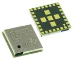
• Module Solution Based on TI's CC2564B DualMode Bluetooth®, Available in Two Variants:
– CC2564MODA With Integrated Antenna
– CC2564MODN With External Antenna
• Fully Certified Module for FCC, IC, CE, and
Bluetooth 4.1
– FCC (Z64-2564N), IC (451I-2564N) Modular
Grant (see Section 6.2.1.3, Section 7.1.1, and
Section 7.1.2)
– CE Certified as Summarized in the Declaration
of Conformity (see Section 7.1.3)
– Bluetooth 4.1 Controller Subsystem Qualified
(CC2564MODN: QDID 55257; CC2564MODA:
QDID 64631). Compliant up to the HCI Layer
• Highly Optimized for Design Into Small Form
Factor Systems and Flexibility:
– CC2564MODA
– Integrated Chip Antenna
– Module Footprint: 35 Terminals, 0.8-mm
Pitch, 7 mm × 14 mm × 1.4 mm (Typical)
– CC2564MODN
– Single-Ended 50-Ω RF Interface
– Module Footprint: 33 Terminals, 0.8-mm
Pitch, 7 mm × 7 mm × 1.4 mm (Typical)
• BR and EDR Features Include:
– Up to Seven Active Devices
– Scatternet: Up to Three Piconets
Simultaneously, One as Master and Two as
Slaves
– Up to Two Synchronous Connection Oriented
(SCO) Links on the Same Piconet
– Support for All Voice Air-Coding—Continuously
Variable Slope Delta (CVSD), A-Law, µ-Law,
and Transparent (Uncoded)
– Assisted Mode for HFP 1.6 Wideband Speech
(WBS) Profile or A2DP Profile to Reduce Host
Processing and Power
– Support of Multiple Bluetooth Profiles With
Enhanced QoS
• Low Energy Features Include:
– Support of up to 10 Simultaneous Connections
– Multiple Sniff Instances Tightly Coupled to
Achieve Minimum Power Consumption
•
•
•
•
– Independent Buffering for Low Energy Allows
Large Numbers of Multiple Connections Without
Affecting BR or EDR Performance
– Built-In Coexistence and Prioritization Handling
for BR, EDR, and Low Energy
Best-in-Class Bluetooth (RF) Performance (TX
Power, RX Sensitivity, Blocking)
– Class 1.5 TX Power up to +10 dBm
– –93 dbm Typical RX Sensitivity
– Internal Temperature Detection and
Compensation to Ensure Minimal Variation in
RF Performance Over Temperature, No
External Calibration Required
– Improved Adaptive Frequency Hopping (AFH)
Algorithm With Minimum Adaptation Time
– Provides Longer Range, Including Twice the
Range of Other Low-Energy-Only Solutions
Advanced Power Management for Extended
Battery Life and Ease of Design
– On-Chip Power Management, Including Direct
Connection to Battery
– Low Power Consumption for Active, Standby,
and Scan Bluetooth Modes
– Shutdown and Sleep Modes to Minimize Power
Consumption
Physical Interfaces:
– UART Interface With Support for Maximum
Bluetooth Data Rates
– UART Transport Layer (H4) With Maximum
Rate of 4 Mbps
– Three-Wire UART Transport Layer (H5) With
Maximum Rate of 4 Mbps
– Fully Programmable Digital Pulse-Code
Modulation (PCM)–I2S Codec Interface
CC256x Bluetooth Hardware Evaluation Tool:
PC-Based Application to Evaluate RF Performance
of the Device and Configure Service Pack
1
An IMPORTANT NOTICE at the end of this data sheet addresses availability, warranty, changes, use in safety-critical applications,
intellectual property matters and other important disclaimers. PRODUCTION DATA.
�CC2564MODN, CC2564MODA
SWRS160E – FEBRUARY 2014 – REVISED JANUARY 2017
1.2
•
•
•
•
•
www.ti.com
Applications
Mobile Accessories
Sports and Fitness Applications
Wireless Audio Solutions
Set-Top Boxes and Remote Controls
Toys
1.3
•
•
•
•
•
Test and Measurement
Industrial: Cable Replacement
Wireless Sensors
Automotive Aftermarket
Wellness and Health
Description
The CC2564MODx module from Texas Instruments™ is a complete Bluetooth® BR/EDR, and low energy
HCI solution that reduces design effort, cost, and time to market. The CC2564MODx module includes TI's
seventh-generation core and provides a versatile, product-proven solution that is Bluetooth 4.1-compliant.
The module is also certified for FCC, IC, and CE, requiring no prior RF experience to develop with this
device; and the device includes a royalty-free software stack compatible with several host MCUs and
MPUs. The CC2564MODx module provides best-in-class RF performance with transmit power and receive
sensitivity that provides twice the range and higher throughput than other Bluetooth-low-energy-only
solutions.
Furthermore, TI’s power-management hardware and software algorithms provide significant power savings
in all commonly used Bluetooth BR/EDR and low energy modes of operation.
The TI dual-mode Bluetooth stack software is certified and provided royalty free for TI's MSP430™ and
MSP432™ ARM® Cortex®-M3 and ARM® Cortex®-M4 MCUs, and Linux® based MPUs. Other processors
can be supported through TI's third party. The iPod® (MFi) protocol is supported by add-on software
packages. Multiple profiles and sample applications, including the following, are supported:
• Serial port profile (SPP)
• Advanced audio distribution profile (A2DP)
• Audio/video remote control profile (AVRCP)
• Hands-free profile (HFP)
• Human interface device (HID)
• Generic attribute profile (GATT)
• Several Bluetooth low energy profiles and services
For more information, see TI Dual-Mode Bluetooth Stack.
In addition to software, the BOOST-CC2564MODA and CC2564MODxEM evaluation boards are available
for each variant. For more information on TI’s wireless platform solutions for Bluetooth, see TI's wirelessconnectivity/dual-mode-bluetooth page.
Device Information (1)
PART NUMBER
CC2564MODNCMOET
PACKAGE
BODY SIZE
MOE (33)
7.0 mm × 7.0 mm × 1.4 mm (Typical)
CC2564MODNCMOER
MOE (33)
7.0 mm × 7.0 mm × 1.4 mm (Typical)
CC2564MODACMOG
MOG (35)
7.0 mm × 14.0 mm × 1.4 mm (Typical)
(1)
For more information on these devices, see Section 8.2.
space
2
Device Overview
Copyright © 2014–2017, Texas Instruments Incorporated
Submit Documentation Feedback
Product Folder Links: CC2564MODN CC2564MODA
�CC2564MODN, CC2564MODA
www.ti.com
1.4
SWRS160E – FEBRUARY 2014 – REVISED JANUARY 2017
Functional Block Diagram
VDD_IN VDD_IO
UART
Antenna
Filter
CC2564B
PCM
nSHUTD
32.768 kHz
Slow Clock
38.4 MHz
XTAL
Figure 1-1. CC2564MODA Functional Block Diagram
VDD_IN VDD_IO
UART
Antenna
Filter
CC2564B
PCM
nSHUTD
32.768 kHz
Slow Clock
38.4 MHz
XTAL
Figure 1-2. CC2564MODN Functional Block Diagram
Copyright © 2014–2017, Texas Instruments Incorporated
Submit Documentation Feedback
Product Folder Links: CC2564MODN CC2564MODA
Device Overview
3
�CC2564MODN, CC2564MODA
SWRS160E – FEBRUARY 2014 – REVISED JANUARY 2017
www.ti.com
Table of Contents
1
2
3
Device Overview ......................................... 1
5.5
Bluetooth low energy Description ................... 20
1.1
Features .............................................. 1
5.6
Bluetooth Transport Layers ......................... 21
1.2
Applications ........................................... 2
5.7
Host Controller Interface
1.3
Description ............................................ 2
5.8
Digital Codec Interface .............................. 23
1.4
Functional Block Diagram ............................ 3
5.9
Assisted Modes
Revision History ......................................... 4
Terminal Configuration and Functions .............. 5
.......................................... 5
3.2
Pin Attributes ......................................... 6
3.3
Connections for Unused Signals ..................... 7
Specifications ............................................ 8
4.1
Absolute Maximum Ratings .......................... 8
4.2
ESD Ratings .......................................... 8
4.3
Power-On Hours ...................................... 8
4.4
Recommended Operating Conditions ................ 8
4.5
Power Consumption Summary ....................... 9
4.6
Electrical Characteristics ............................ 10
4.7
Timing and Switching Characteristics ............... 11
Detailed Description ................................... 19
5.1
Overview ............................................ 19
5.2
Functional Block Diagram ........................... 19
5.3
Functional Blocks ................................... 20
5.4
Bluetooth BR and EDR Description ................. 20
3.1
4
5
6
Pin Diagram
7
8
............................
.....................................
21
25
Applications, Implementation, and Layout........ 31
.....................
..............................................
6.3
Soldering Recommendations .......................
Device and Documentation Support ...............
7.1
Device Certification and Qualification ...............
7.2
Tools and Software .................................
7.3
Device Nomenclature ...............................
7.4
Documentation Support .............................
7.5
Related Links ........................................
7.6
Community Resources ..............................
7.7
Trademarks..........................................
7.8
Electrostatic Discharge Caution .....................
7.9
Glossary .............................................
6.1
Reference Design Schematics
31
6.2
Layout
32
42
43
43
43
46
46
48
48
48
48
48
Mechanical, Packaging, and Orderable
Information .............................................. 49
....................................
............................
8.1
Mechanical Data
8.2
Packaging and Ordering
49
51
2 Revision History
NOTE: Page numbers for previous revisions may differ from page numbers in the current version.
Changes from December 28, 2015 to January 16, 2017
•
•
•
•
•
•
Page
Changed Section 1.1 ................................................................................................................. 1
Changed Section 1.3 ................................................................................................................ 2
Added Table 3-2 ...................................................................................................................... 7
Changed Section 7 .................................................................................................................. 43
Added Figure 7-1 .................................................................................................................... 46
Changed Table 8-1.................................................................................................................. 51
Changes from November 4, 2015 to December 28, 2015
•
•
•
•
•
•
•
•
•
•
•
4
Page
Added CC2564MODA device variant ............................................................................................. 1
Added applications in Section 1.2 ................................................................................................. 2
Changed VBAT to VDD_IN Figure 5-1 and Figure 5-2 .......................................................................... 3
Changed storage temperature range in Section 4.1 ............................................................................. 8
Changed restrictions on verification of parameters in Section 4.7.4.1 ....................................................... 15
Changed restrictions on verification of parameters in Section 4.7.4.2 ....................................................... 18
Changed values for Adjacent channel power |M-N| = 2 and Adjacent channel power |M-N| > 2 in Table 4-15 ........ 18
Added "Includes a 128-bit hardware encryption accelerator as defined by the Bluetooth specifications" in
Section 5.4 ........................................................................................................................... 20
Changed Figure 5-10 .............................................................................................................. 29
Changed Figure 5-11 ............................................................................................................... 30
Changed Section 6.2.2.1 .......................................................................................................... 41
Revision History
Copyright © 2014–2017, Texas Instruments Incorporated
Submit Documentation Feedback
Product Folder Links: CC2564MODN CC2564MODA
�CC2564MODN, CC2564MODA
www.ti.com
SWRS160E – FEBRUARY 2014 – REVISED JANUARY 2017
3 Terminal Configuration and Functions
3.1
Pin Diagram
GND
13
14
NC
15
GND
16
nSHUTD
17
GND
GND
TX_DBG
CC2564MODA
SLOW_CLK_IN
11
10
9
8
7
NC
GND
12
6
HCI_RTS
GND
4
GNDPAD
GNDPAD
GNDPAD
GNDPAD
GNDPAD
GNDPAD
GNDPAD
GNDPAD
GNDPAD
GNDPAD
GNDPAD
1
25
26
27
28
29
30
31
32
33
34
35
NC
NC
5
24
NC
AUD_FSYNC
HCI_RX
23
VDD_IN
AUD_CLK
3
22
AUD_OUT
HCI_TX
21
AUD_IN
2
20
HCI_CTS
19
VDD_IO
18
Figure 3-1 shows the top view of the terminal designations for the CC2564MODA device.
SWRS160-006
Figure 3-1. CC2564MODA Pin Diagram (Top View)
21
22
23
24
GND
13
14
BT_ANT
15
GND
17
16
nSHUTD
AUD_IN
AUD_OUT
GND
19
20
VDD_IO
18
Figure 3-2 shows the top view of the terminal designations for the CC2564MODN device.
VDD_IN
AUD_CLK
NC
AUD_FSYNC
NC
NC
GND
TX_DBG
CC2564MODN
SLOW_CLK_IN
10
9
8
7
NC
GND
11
6
HCI_RTS
4
5
HCI_RX
3
2
HCI_TX
GND
HCI_CTS
GNDPAD
GNDPAD
GNDPAD
GNDPAD
GNDPAD
GNDPAD
GNDPAD
GNDPAD
GNDPAD
1
25
26
27
28
29
30
31
32
33
12
SWRS160-006
Figure 3-2. CC2564MODN Pin Diagram (Top View)
Terminal Configuration and Functions
Submit Documentation Feedback
Product Folder Links: CC2564MODN CC2564MODA
Copyright © 2014–2017, Texas Instruments Incorporated
5
�CC2564MODN, CC2564MODA
SWRS160E – FEBRUARY 2014 – REVISED JANUARY 2017
3.2
www.ti.com
Pin Attributes
Table 3-1 describes the pin attributes.
Table 3-1. Pin Attributes
NO.
NAME
ESD (1) (V)
PULL AT
RESET
DEF.
DIR. (2)
I/O
Type (3)
DESCRIPTION
1
HCI_CTS
750
PU
I
8 mA
HCI UART clear-to-send. The device can send data
when HCI_CTS is low.
2
HCI_TX
750
PU
O
8 mA
HCI UART data transmit
3
HCI_RX
750
PU
I
8 mA
HCI UART data receive
4
HCI_RTS
750
PU
O
8 mA
HCI UART request-to-send. Host can send data when
HCI_RTS is low.
5
GND
1000
Ground
7
GND
1000
Ground
8
SLOW_CLK_IN
1000
9
GND
1000
12
VDD_IN
13
GND
14
BT_ANT
I
32.768-kHz clock in
Fail-safe
Ground
I
Main power supply for the module (2.2 to 4.8 V)
Ground
500
I/O
Bluetooth RF I/O (CC2564MODN only)
NC
Not connected (CC2564MODA only)
15
GND
Ground
16
nSHUTD
17
GND
18
VDD_IO
1000
19
AUD_IN
500
PD
I
4 mA
PCM data input
Fail-safe
20
AUD_OUT
500
PD
O
4 mA
PCM data output
Fail-safe
21
AUD_CLK
500
PD
I/O
HY, 4 mA
PCM clock
Fail-safe
22
AUD_FSYNC
500
PD
I/O
4 mA
PCM frame sync
Fail-safe
2 mA
TI internal debug messages. TI
recommends leaving a test point.
PD
I
Shutdown input (active low)
Ground
I
24
TX_DBG
1000
25
GNDPAD
1000
Ground
26
GNDPAD
1000
Ground
27
GNDPAD
1000
Ground
28
GNDPAD
1000
Ground
29
GNDPAD
1000
Ground
30
GNDPAD
1000
Ground
31
GNDPAD
1000
Ground
32
GNDPAD
1000
Ground
33
GNDPAD
1000
Ground
34
GNDPAD
1000
Ground (CC2564MODA only)
35
GNDPAD
1000
Ground (CC2564MODA only)
(1)
(2)
(3)
6
PU
O
I/O power supply (1.8 V nominal)
ESD: Human Body Model (HBM). JEDEC 22-A114 2-wire method. CDM: All pins pass 500 V except BT_ANT, which passes 400 V.
I = input; O = output; I/O = bidirectional
I/O Type: Digital I/O cells. HY = input hysteresis, current = typical output current
Terminal Configuration and Functions
Copyright © 2014–2017, Texas Instruments Incorporated
Submit Documentation Feedback
Product Folder Links: CC2564MODN CC2564MODA
�CC2564MODN, CC2564MODA
www.ti.com
3.3
SWRS160E – FEBRUARY 2014 – REVISED JANUARY 2017
Connections for Unused Signals
Table 3-2 lists the connections for unused signals.
Table 3-2. Connections for Unused Signals
PIN
NUMBER
FUNCTION
ESD (1)
(V)
PULL AT
RESET
DEF. DIR. (2)
I/O
Type (3)
DESCRIPTION
6
NC
I
Not connected
10
NC
O
Not connected
11
NC
O
23
NC
(1)
(2)
(3)
500
PD
I/O
Not connected
4 mA
Not connected
ESD: Human Body Model (HBM). JEDEC 22-A114 2-wire method. CDM: All pins pass 500 V except BT_ANT, which passes 400 V.
I = input; O = output; I/O = bidirectional
I/O Type: Digital I/O cells. HY = input hysteresis, current = typical output current
Terminal Configuration and Functions
Submit Documentation Feedback
Product Folder Links: CC2564MODN CC2564MODA
Copyright © 2014–2017, Texas Instruments Incorporated
7
�CC2564MODN, CC2564MODA
SWRS160E – FEBRUARY 2014 – REVISED JANUARY 2017
www.ti.com
4 Specifications
Unless otherwise indicated, all measurements are taken at the device pins of the TI test evaluation board
(EVB). All specifications are over process, voltage, and temperature, unless otherwise indicated.
All values apply to the CC2564MODA and CC2564MODN devices, unless otherwise indicated.
4.1
Absolute Maximum Ratings
Over operating free-air temperature range (unless otherwise indicated). All parameters are measured as follows: VDD_IN =
3.6 V and VDD_IO = 1.8 V (unless otherwise indicated). (1)
VDD_IN
Supply voltage
VDD_IO
Input voltage to analog pins
(2)
MIN
MAX
–0.5
4.8
V
–0.5
2.145
V
V
–0.5
2.1
Input voltage to all other pins
–0.5
VDD_IO + 0.5
V
Operating ambient temperature (3)
–30
85
°C
10
dBm
–40
100
°C
Bluetooth RF inputs
Tstg
(1)
(2)
(3)
UNIT
Storage temperature
Stresses beyond those listed under Absolute Maximum Ratings may cause permanent damage to the device. These are stress ratings
only and functional operation of the device at these or any other conditions beyond those indicated under Recommended Operating
Conditions is not implied. Exposure to absolute-maximum-rated conditions for extended periods may affect device reliability.
Analog pin: BT_ANT
The module supports a temperature range of –30°C to +85°C because of the operating conditions of the crystal.
4.2
ESD Ratings
VALUE UNIT
V(ESD)
(1)
(2)
Electrostatic discharge
Human body model (HBM), per ANSI/ESDA/JEDEC JS-001 (1)
±500
Charged device model (CDM), per JEDEC specification JESD22C101 (2)
±500
JEDEC document JEP155 states that 500-V HBM allows safe manufacturing with a standard ESD control process.
JEDEC document JEP157 states that 250-V CDM allows safe manufacturing with a standard ESD control process.
Power-On Hours (1)
4.3
DEVICE
CONDITIONS
Duty cycle = 25% active and 75% sleep
TA = 70ºC
CC2564MODx
(1)
POWER-ON HOURS
15,400 (7 years)
This information is provided solely to give the customer an estimation of the POH under certain specified conditions, and is not intended
to – and does not – extend the warranty for the device under TI’s Standard Terms and Conditions.
4.4
Recommended Operating Conditions
MIN
MAX
2.2
4.8
V
1.62
1.92
V
Condition: Default
0.65 × VDD_IO
VDD_IO
V
Condition: Default
0
0.35 ×
VDD_IO
V
I/O input rise and fall times,10% to 90% — asynchronous mode
1
10
ns
I/O input rise and fall times, 10% to 90% — synchronous mode
(PCM)
1
2.5
ns
400
mV
85
°C
VDD_IN
Power supply voltage
VDD_IO
I/O power supply voltage
VIH
High-level input voltage
VIL
Low-level input voltage
tr and tf
Voltage dips on VDD_IN (V(BAT))
duration = 577 µs to 2.31 ms, period = 4.6 ms
Maximum ambient operating temperature
(1)
8
V
(1)
–30
UNIT
A crystal-based solution is limited by the temperature range required for the crystal to meet 20 ppm.
Specifications
Copyright © 2014–2017, Texas Instruments Incorporated
Submit Documentation Feedback
Product Folder Links: CC2564MODN CC2564MODA
�CC2564MODN, CC2564MODA
www.ti.com
4.5
SWRS160E – FEBRUARY 2014 – REVISED JANUARY 2017
Power Consumption Summary
4.5.1
Static Current Consumption
OPERATIONAL MODE
Shutdown mode
MIN
TYP
(1)
Deep sleep mode (2)
UNIT
1
7
40
105
µA
1
mA
107
mA
112.5
mA
Total I/O current consumption in active mode
Continuous transmission—GFSK (3)
Continuous transmission—EDR (4) (5)
(1)
(2)
(3)
(4)
(5)
MAX
µA
V(BAT) + VIO + V(SHUTDOWN)
V(BAT) + VIO
At maximum output power (10 dBm)
At maximum output power (8 dBm)
Both π / 4 DQPSK and 8DPSK
4.5.2
Dynamic Current Consumption
4.5.2.1
Current Consumption for Different Bluetooth BR and EDR Scenarios
Conditions: VDD_IN = 3.6 V, 25°C, nominal unit, 8-dBm output power
OPERATIONAL MODE
MASTER AND SLAVE
AVERAGE CURRENT
UNIT
Synchronous connection oriented (SCO) link HV3
Master and slave
13.7
mA
Extended SCO (eSCO) link EV3 64 kbps, no retransmission
Master and slave
13.2
mA
eSCO link 2-EV3 64 kbps, no retransmission
Master and slave
10
mA
GFSK full throughput: TX = DH1, RX = DH5
Master and slave
40.5
mA
EDR full throughput: TX = 2-DH1, RX = 2-DH5
Master and slave
41.2
mA
EDR full throughput: TX = 3-DH1, RX = 3-DH5
Master and slave
41.2
mA
Sniff, four attempts, 1.28 seconds
Master and slave
145
µA
Page or inquiry scan 1.28 seconds, 11.25 ms
Master and slave
320
µA
Page (1.28 seconds) and inquiry (2.56 seconds) scans,
11.25 ms
Master and slave
445
µA
A2DP source
Master
13.9
mA
A2DP sink
Master
15.2
mA
Assisted A2DP source
Master
16.9
mA
Assisted A2DP sink
Master
18.1
mA
Assisted WBS EV3; retransmit effort = 2;
maximum latency = 8 ms
Master and slave
17.5 and 18.5
mA
Assisted WBS 2EV3; retransmit effort = 2;
maximum latency = 12 ms
Master and slave
11.9 and 13
mA
Copyright © 2014–2017, Texas Instruments Incorporated
Submit Documentation Feedback
Product Folder Links: CC2564MODN CC2564MODA
Specifications
9
�CC2564MODN, CC2564MODA
SWRS160E – FEBRUARY 2014 – REVISED JANUARY 2017
4.5.2.2
www.ti.com
Current Consumption for Different Low Energy Scenarios
Conditions: VDD_IN = 3.6 V, 25°C, nominal unit, 8-dBm output power
MODE
DESCRIPTION
AVERAGE
CURRENT
UNIT
Advertising, nonconnectable
Advertising in all three channels
1.28-seconds advertising interval
15 bytes advertise data
114
µA
Advertising, discoverable
Advertising in all three channels
1.28-seconds advertising interval
15 bytes advertise data
138
µA
Scanning
Listening to a single frequency per window
1.28-seconds scan interval
11.25-ms scan window
324
µA
Connected (master role)
500-ms connection interval
0-ms slave connection latency
Empty TX and RX LL packets
Connected (slave role)
4.6
µA
199 (slave)
Electrical Characteristics
RATING
CONDITION
High-level output voltage, VOH
Low-level output voltage, VOL
I/O input impedance
MIN
MAX
At 2, 4, 8 mA
0.8 × VDD_IO
VDD_IO
At 0.1 mA
VDD_IO – 0.2
VDD_IO
At 2, 4, 8 mA
0
0.2 × VDD_IO
At 0.1 mA
0
0.2
Resistance
1
Capacitance
Output rise and fall times, 10% to 90% (digital pins)
PCM-I2S bus, TX_DBG
I/O pull currents
All others
10
169 (master)
Specifications
CL = 20 pF
UNIT
V
V
MΩ
5
pF
10
ns
PU
Typical = 6.5
3.5
9.7
PD
Typical = 27
9.5
55
PU
Typical = 100
50
300
PD
Typical = 100
50
360
µA
µA
Copyright © 2014–2017, Texas Instruments Incorporated
Submit Documentation Feedback
Product Folder Links: CC2564MODN CC2564MODA
�CC2564MODN, CC2564MODA
www.ti.com
4.7
SWRS160E – FEBRUARY 2014 – REVISED JANUARY 2017
Timing and Switching Characteristics
4.7.1
Device Power Supply
The power-management hardware and software algorithms of the TI Bluetooth HCI module provide
significant power savings, which is a critical parameter in an MCU-based system.
The power-management module is optimized for drawing extremely low currents.
4.7.1.1
Power Sources
The TI Bluetooth HCI module requires two power sources:
• VDD_IN: main power supply for the module
• VDD_IO: power source for the 1.8-V I/O ring
The HCI module includes several on-chip voltage regulators for increased noise immunity and can be
connected directly to the battery.
4.7.1.2
Power Supply Sequencing
The device includes the following power-up requirements (see Figure 4-1):
• nSHUTD must be low. VDD_IN and VDD_IO are don't-care when nSHUTD is low. However, signals
are not allowed on the I/O pins if I/O power is not supplied, because the I/Os are not fail-safe.
Exceptions are SLOW_CLK_IN and AUD_xxx, which are fail-safe and can tolerate external voltages
with no VDD_IO and VDD_IN.
• VDD_IO and VDD_IN must be stable before releasing nSHUTD.
• The slow clock must be stable within 2 ms of nSHUTD going high.
The device indicates that the power-up sequence is complete by asserting RTS low, which occurs up to
100 ms after nSHUTD goes high. If RTS does not go low, the device is not powered up. In this case,
ensure that the sequence and requirements are met.
Shut down
before
VDD_IO
removed
20 µs maximum
nSHUTD
VDD_IO
VDD_IN
2 ms maximum
slow clock
±100 ms
HCI_RTS
CC256x ready
SWRS160-008
Figure 4-1. Power-Up and Power-Down Sequence
Copyright © 2014–2017, Texas Instruments Incorporated
Submit Documentation Feedback
Product Folder Links: CC2564MODN CC2564MODA
Specifications
11
�CC2564MODN, CC2564MODA
SWRS160E – FEBRUARY 2014 – REVISED JANUARY 2017
4.7.1.3
www.ti.com
Power Supplies and Shutdown – Static States
The nSHUTD signal puts the device in ultra-low power mode and performs an internal reset to the device.
The rise time for nSHUTD must not exceed 20 µs; nSHUTD must be low for a minimum of 5 ms.
To prevent conflicts with external signals, all I/O pins are set to the high-impedance (Hi-Z) state during
shutdown and power up of the device. The internal pull resistors are enabled on each I/O pin, as
described in Section 3.2. Table 4-1 describes the static operation states.
Table 4-1. Power Modes
VDD_IN
(1)
(1)
VDD_IO
(1)
nSHUTD (1)
PM_MODE
COMMENTS
1
None
None
Asserted
Shutdown
I/O state is undefined. I/O voltages are
not allowed on nonfail-safe pins.
2
None
None
Deasserted
Not allowed
I/O state is undefined. I/O voltages are
not allowed on nonfail-safe pins.
3
None
Present
Asserted
Shutdown
4
None
Present
Deasserted
Not allowed
5
Present
None
Asserted
Shutdown
6
Present
None
Deasserted
Not allowed
7
Present
Present
Asserted
Shutdown
8
Present
Present
Deasserted
Active
I/Os are defined as tri-state with
internal pullup or pulldown enabled.
I/O state is undefined. I/O voltages are
not allowed on nonfail-safe pins.
I/O state is undefined.
I/O state is undefined. I/O voltages are
not allowed on nonfail-safe pins.
I/Os are defined as tri-state with
internal pullup or pulldown enabled.
See Section 4.7.1.4
The terms None or Asserted can imply any of the following conditions: directly pulled to ground or driven low, pulled to ground through a
pulldown resistor, or left NC or floating (high-impedance output stage).
4.7.1.4
I/O States in Various Power Modes
CAUTION
Some device I/Os are not fail-safe (see Section 3.2). Fail-safe means that the
pins do not draw current from an external voltage applied to the pin when I/O
power is not supplied to the device. External voltages are not allowed on these
I/O pins when the I/O supply voltage is not supplied because of possible
damage to the device.
Table 4-2 lists the I/O states in various power modes.
Table 4-2. I/O States in Various Power Modes
I/O NAME
SHUT DOWN (1)
DEFAULT ACTIVE (1)
I/O State
Pull
HCI_RX
Z
HCI_TX
Z
HCI_RTS
DEEP SLEEP (1)
I/O State
Pull
PU
I
PU
PU
O-H
O
Z
PU
O-H
O
HCI_CTS
Z
PU
I
PU
I
PU
AUD_CLK
Z
PD
I
PD
I
PD
AUD_FSYNC
Z
PD
I
PD
I
PD
AUD_IN
Z
PD
I
PD
I
PD
AUD_OUT
Z
PD
Z
PD
Z
PD
TX_DBG
Z
PU
O
(1)
12
I/O State
Pull
I
PU
I = input, O = output, Z = Hi-Z, — = no pull, PU = pullup, PD = pulldown, H = high, L = low
Specifications
Copyright © 2014–2017, Texas Instruments Incorporated
Submit Documentation Feedback
Product Folder Links: CC2564MODN CC2564MODA
�CC2564MODN, CC2564MODA
www.ti.com
4.7.1.5
SWRS160E – FEBRUARY 2014 – REVISED JANUARY 2017
nSHUTD Requirements
Table 4-3. nSHUTD Requirements
PARAMETER
VIH
VIL
MIN
MAX
UNIT
Operation mode level
(1)
1.42
1.98
V
Shutdown mode level
(1)
0
0.4
Minimum time for nSHUT_DOWN low to reset the device
tr and tf
(1)
V
5
ms
Rise and fall times
20
µs
An internal 300-kΩ pulldown retains shut-down mode when no external signal is applied to this pin.
4.7.2
Clock Specifications
Table 4-4. Slow Clock Requirements
CHARACTERISTICS
CONDITION
MIN
Input slow clock frequency
Input slow clock accuracy
(Initial + temp + aging)
tr and
tf
TYP
32768
Bluetooth
ANT
±50
200
Frequency input duty cycle
15%
VIH
Square wave, DC-coupled
ppm
ns
85%
0.65 ×
VDD_IO
VDD_IO
V peak
0
0.35 ×
VDD_IO
V peak
VIL
Input impedance
1
Input capacitance
4.7.3
50%
UNIT
Hz
±250
Input transition time tr and tf
(10% to 90%)
Slow clock input voltage limits
MAX
MΩ
5
pF
Peripherals
4.7.3.1
UART
Figure 4-2 shows the UART timing diagram.
HCI_RTS
t2
t1
HCI_RX
t6
HCI_CTS
t3
t4
HCI_TX
Start bit
Stop bit
10 bits
td_uart_swrs064
Figure 4-2. UART Timing
Copyright © 2014–2017, Texas Instruments Incorporated
Submit Documentation Feedback
Product Folder Links: CC2564MODN CC2564MODA
Specifications
13
�CC2564MODN, CC2564MODA
SWRS160E – FEBRUARY 2014 – REVISED JANUARY 2017
www.ti.com
Table 4-5 lists the UART timing characteristics.
Table 4-5. UART Timing Characteristics
SYMBOL
CHARACTERISTICS
CONDITION
MIN
Baud rate
MAX
UNIT
37.5
TYP
4000
kbps
Baud rate accuracy per byte
Receive and transmit
–2.5
1.5%
Baud rate accuracy per bit
Receive and transmit
–12.5
12.5%
t3
CTS low to TX_DATA on
t4
CTS high to TX_DATA off
t6
CTS-high pulse width
t1
RTS low to RX_DATA on
t2
RTS high to RX_DATA off
0
2
Hardware flow control
µs
1
1
0
byte
bit
2
Interrupt set to 1/4 FIFO
µs
16
byte
Figure 4-3 shows the UART data frame.
tb
TX
D0
STR
D1
Dn
D2
PAR
STP
td_uart_swrs064
Figure 4-3. Data Frame
Table 4-6 describes the symbols used in Figure 4-3.
Table 4-6. Data Frame Key
SYMBOL
4.7.3.2
DESCRIPTION
STR
Start bit
D0...Dn
Data bits (LSB first)
PAR
Parity bit (optional)
STP
Stop bit
PCM
Figure 4-4 shows the interface timing for the PCM.
Tclk
Tw
Tw
AUD_CLK
tis
tih
AUD_IN / FSYNC_IN
top
AUD_OUT / FSYNC_OUT
td_aud_swrs064
Figure 4-4. PCM Interface Timing
14
Specifications
Copyright © 2014–2017, Texas Instruments Incorporated
Submit Documentation Feedback
Product Folder Links: CC2564MODN CC2564MODA
�CC2564MODN, CC2564MODA
www.ti.com
SWRS160E – FEBRUARY 2014 – REVISED JANUARY 2017
Table 4-7 lists the associated PCM master parameters.
Table 4-7. PCM Master
SYMBOL
PARAMETER
Tclk
Cycle time
Tw
High or low pulse width
CONDITION
MIN
MAX
244.14
(4.096 MHz)
15625
(64 kHz)
UNIT
ns
50% of Tclk min
ns
ns
tis
AUD_IN setup time
25
tih
AUD_IN hold time
0
top
AUD_OUT propagation time
40-pF load
0
10
ns
top
FSYNC_OUT propagation time
40-pF load
0
10
ns
MIN
MAX
ns
Table 4-8 lists the associated PCM slave parameters.
Table 4-8. PCM Slave
SYMBOL
PARAMETER
CONDITION
UNIT
66.67
(15 MHz)
ns
Tclk
Cycle time
Tw
High or low pulse width
40% of Tclk
ns
Tis
AUD_IN setup time
8
ns
Tih
AUD_IN hold time
0
ns
ns
tis
AUD_FSYNC setup time
8
tih
AUD_FSYNC hold time
0
top
AUD_OUT propagation time
4.7.4
40-pF load
0
ns
21
ns
RF Performance
4.7.4.1
Bluetooth BR and EDR RF Performance
All parameters in this section are verified using a 38.4-MHz XTAL and an RF load of 50 Ω at the BT_ANT
port. These parameters are verified in a conducted mode and do not include antenna performance.
Table 4-9. Bluetooth Receiver—In-Band Signals
CHARACTERISTICS
CONDITION
Operation frequency range
MIN
TYP
2402
1
Input impedance
50
GFSK, BER = 0.1%
BER error floor at sensitivity + 10
dB, dirty TX off
Intermodulation characteristics
(1)
MHz
Ω
–70
π /4-DQPSK, BER = 0.01%
–92.5
–70
8DPSK, BER = 0.01%
–85.5
–70
π / 4-DQPSK
1E–7
1E–5
8DPSK
UNIT
MHz
–93
dBm
1E–5
GFSK, BER = 0.1%
Maximum usable input power
BLUETOOTH
SPECIFICATION
2480
Channel spacing
Sensitivity, dirty TX on (1)
MAX
–5
π / 4-DQPSK, BER = 0.1%
–10
8DPSK, BER = 0.1%
–10
Level of interferers (for n = 3, 4, and 5)
–20
dBm
–30
–39
dBm
Sensitivity degradation up to 3 dB may occur for minimum and typical values where the Bluetooth frequency is a harmonic of the fast
clock.
Copyright © 2014–2017, Texas Instruments Incorporated
Submit Documentation Feedback
Product Folder Links: CC2564MODN CC2564MODA
Specifications
15
�CC2564MODN, CC2564MODA
SWRS160E – FEBRUARY 2014 – REVISED JANUARY 2017
www.ti.com
Table 4-9. Bluetooth Receiver—In-Band Signals (continued)
CHARACTERISTICS
CONDITION
MIN
TYP
GFSK, co-channel
EDR, co-channel
8
11
13
16.5
21
–10
0
–10
0
GFSK, adjacent ±1 MHz
EDR, adjacent ±1 MHz, (image)
π / 4-DQPSK
8DPSK
–5
5
–38
–30
π / 4-DQPSK
–38
–30
8DPSK
–38
–25
GFSK, adjacent +2 MHz
C/I performance (2)
Image = –1 MHz
EDR, adjacent, +2 MHz
GFSK, adjacent –2 MHz
EDR, adjacent –2 MHz
–28
–20
π / 4-DQPSK
–28
–20
8DPSK
–22
–13
GFSK, adjacent ≥ |±3| MHz
EDR, adjacent ≥ |±3| MHz
–45
–40
π / 4-DQPSK
–45
–40
8DPSK
–44
–33
RF return loss
RX mode LO leakage
(2)
BLUETOOTH
SPECIFICATION
9.5
π / 4-DQPSK
8DPSK
MAX
Frf = (received RF – 0.6 MHz)
UNIT
dB
–10
dB
–63
dBm
Numbers show ratio of desired signal to interfering signal. Smaller numbers indicate better C/I performance.
Table 4-10. Bluetooth Transmitter—GFSK
CHARACTERISTICS
Maximum RF output power
MIN
TYP
(1)
MAX
BLUETOOTH
SPECIFICATION
10
Gain control range
dBm
30
Power control step
2
8
2 to 8
Adjacent channel power |M–N| = 2
–35
≤ –20
Adjacent channel power |M–N| > 2
–45
≤ –40
(1)
UNIT
dB
dBm
To modify maximum output power, use an HCI VS command.
Table 4-11. Bluetooth Transmitter—EDR
CHARACTERISTICS
EDR output
power
MIN
TYP
π / 4-DQPSK
VDD_IN = V(BAT)
8
8DPSK
VDD_IN = V(BAT)
8
EDR relative power
–2
Gain control range
MAX
BLUETOOTH
SPECIFICATION
dBm
1
–4 to +1
30
Power control step
2
UNIT
dB
8
2 to 8
Adjacent channel power |M–N| = 1
–30
≤ –26
dBc
Adjacent channel power |M–N| = 2
–23
≤ –20
dBm
–42
≤ –40
dBm
Adjacent channel power |M–N| > 2
(1)
16
(1)
Adjacent channel power measurements take into account specification exception of three bands, as defined by the Test Suite Structure
(TSS) and Test Purposes (TP) Bluetooth Documentation Specification.
Specifications
Copyright © 2014–2017, Texas Instruments Incorporated
Submit Documentation Feedback
Product Folder Links: CC2564MODN CC2564MODA
�CC2564MODN, CC2564MODA
www.ti.com
SWRS160E – FEBRUARY 2014 – REVISED JANUARY 2017
Table 4-12. Bluetooth Modulation—GFSK
CHARACTERISTICS
–20 dB bandwidth
F1
avg
F2
max
Modulation
characteristics
CONDITION
MIN
TYP
UNIT
925
≤ 1000
kHz
Δf1avg
165
140 to 175
kHz
Δf2max ≥ limit for at least
99.9% of all Δf2max
Mod data =
1010101...
130
> 115
kHz
88%
> 80%
DH1
–25
25
< ±25
DH3 and DH5
–35
35
< ±40
20
< 20
kHz/
50 µs
+75
< ±75
kHz
Drift rate
Initial carrier frequency
tolerance
BLUETOOTH
SPECIFICATION
Mod data = 4 1s,
4 0s:
111100001111...
GFSK
Δf2avg, Δf1avg
Absolute carrier
frequency drift
MAX
f0–fTX
–75
kHz
Table 4-13. Bluetooth Modulation—EDR
CHARACTERISTICS
CONDITION
MIN
TYP
MAX
BLUETOOTH
SPECIFICATION
UNIT
Carrier frequency stability
–10
10
≤ 10
kHz
Initial carrier frequency tolerance
–75
75
±75
kHz
RMS DEVM
(1)
99% DEVM (1)
Peak DEVM
(1)
(1)
π / 4-DQPSK
6%
8DPSK
6%
20%
13%
π / 4-DQPSK
30%
30%
8DPSK
20%
20%
π / 4-DQPSK
14%
35%
8DPSK
16%
25%
MAX performance refers to maximum TX power.
Copyright © 2014–2017, Texas Instruments Incorporated
Submit Documentation Feedback
Product Folder Links: CC2564MODN CC2564MODA
Specifications
17
�CC2564MODN, CC2564MODA
SWRS160E – FEBRUARY 2014 – REVISED JANUARY 2017
4.7.4.2
www.ti.com
Bluetooth low energy RF Performance
All parameters in this section are verified using a 38.4-MHz XTAL and an RF load of 50 Ω at the BT_ANT
port. These parameters are verified in a conducted mode and do not include antenna performance.
Table 4-14. Bluetooth low energy Receiver—In-Band Signals
CHARACTERISTICS
CONDITION
Operation frequency range
MIN
TYP
2402
2480
Channel spacing
2
Input impedance
50
Sensitivity, dirty TX on (1)
PER = 30.8%; dirty TX on
Maximum usable input power
GMSK, PER = 30.8%
Intermodulation characteristics
Level of interferers
(for n = 3, 4, 5)
GMSK, co-channel
C/I performance (2)
Image = –1 MHz
RX mode LO leakage
(1)
(2)
BLUETOOTH
low energy
SPECIFICATION
MAX
UNIT
MHz
MHz
Ω
≤ –70
dBm
≥ –10
dBm
–30
≥ –50
dBm
8
≤ 21
–93
–10
GMSK, adjacent ±1 MHz
–5
≤ 15
GMSK, adjacent +2 MHz
–45
≤ –17
GMSK, adjacent –2 MHz
–22
≤ –15
GMSK, adjacent ≥ |±3| MHz
–47
≤ –27
Frf = (received RF – 0.6 MHz)
–63
dB
dBm
Sensitivity degradation up to 3 dB may occur where the Bluetooth low energy frequency is a harmonic of the fast clock.
Numbers show wanted signal-to-interfering signal ratio. Smaller numbers indicate better C/I performance.
Table 4-15. Bluetooth low energy Transmitter
CHARACTERISTICS
MIN
TYP
BLUETOOTH
low energy
SPECIFICATION
MAX
CC2564MODN
10
≤10
CC2564MODA
8 (2)
≤10
Adjacent channel power |M-N| = 2
–35
≤ –20
Adjacent channel power |M-N| > 2
–45
≤ –30
RF output power (VDD_IN = VBAT) (1)
(1)
(2)
UNIT
dBm
dBm
To modify maximum output power, use an HCI VS command.
Required to meet the power spectral density (PSD) as defined by clause 5.3.3.2 in ETSI EN 300 328 V1.9.1. The integrated antenna
gain is 1.69 dBi.
Table 4-16. Bluetooth low energy Modulation
CHARACTERISTICS
Δf1 avg
Modulation
Δf2 max characteristics
Absolute carrier frequency
drift
CONDITION
MIN
Mod data = 4 1s, 4 0s:
1111000011110000...
TYP
18
Specifications
BLUETOOTH
low energy
SPECIFICATION
UNIT
250
225 to 275
kHz
Δf2max ≥ limit for at least Mod data =
99.9% of all Δf2max
1010101...
210
≥ 185
kHz
Δf2avg, Δf1avg
0.9
≥ 0.8
Δf1avg
–25
Drift rate
Initial carrier frequency
tolerance
MAX
–25
25
≤ ±50
kHz
15
≤ 20
kHz/
50 ms
25
≤ ±100
kHz
Copyright © 2014–2017, Texas Instruments Incorporated
Submit Documentation Feedback
Product Folder Links: CC2564MODN CC2564MODA
�CC2564MODN, CC2564MODA
www.ti.com
SWRS160E – FEBRUARY 2014 – REVISED JANUARY 2017
5 Detailed Description
5.1
Overview
Table 5-1. Technology and Assisted Modes Supported
ASSISTED MODES
SUPPORTED (1)
TECHNOLOGY SUPPORTED
MODULE
CC2564MODx (2)
(1)
(2)
5.2
DESCRIPTION
BR/EDR
LE
Bluetooth 4.1 + Bluetooth low energy
√
√
Bluetooth 4.1 + ANT
√
ANT
HFP 1.6
(WBS)
A2DP
√
√
√
√
√
The assisted modes (HFP 1.6 and A2DP) are not supported simultaneously. Furthermore, the assisted modes are not supported
simultaneously with Bluetooth low energy or ANT.
The device does not support simultaneous operation of LE and ANT.
Functional Block Diagram
VDD_IN VDD_IO
UART
Antenna
PCM
CC2564B
Filter
nSHUTD
32.768 kHz
Slow Clock
38.4 MHz
XTAL
Figure 5-1. CC2564MODN Functional Block Diagram
VDD_IN VDD_IO
UART
Antenna
Filter
CC2564B
PCM
nSHUTD
32.768 kHz
Slow Clock
38.4 MHz
XTAL
Figure 5-2. CC2564MODA Functional Block Diagram
Copyright © 2014–2017, Texas Instruments Incorporated
Submit Documentation Feedback
Product Folder Links: CC2564MODN CC2564MODA
Detailed Description
19
�CC2564MODN, CC2564MODA
SWRS160E – FEBRUARY 2014 – REVISED JANUARY 2017
5.3
www.ti.com
Functional Blocks
The TI Bluetooth HCI module architecture comprises a DRP and a point-to-multipoint baseband core. The
architecture is based on a single-processor ARM® ARM7TDMI™ core. The module includes several onchip peripherals to enable easy communication with a host system and the Bluetooth BR/EDR/LE core.
5.4
Bluetooth BR and EDR Description
The CC2564MODx is Bluetooth 4.1 compliant up to the HCI level (for the technology supported, see
Table 5-1):
• Up to seven active devices
• Scatternet: Up to 3 piconets simultaneously, 1 as master and 2 as slaves
• Up to two synchronous connection oriented (SCO) links on the same piconet
• Very fast AFH algorithm for asynchronous connection-oriented link (ACL) and extended SCO (eSCO)
link
• Supports typically 10-dBm TX power without an external power amplifier (PA), thus improving
Bluetooth link robustness
• Digital radio processor (DRP™) single-ended 50-Ω I/O for easy RF interfacing with external antenna
(CC2564MODN). The CC2564MODA includes the antenna on the module.
• Internal temperature detection and compensation to ensure minimal variation in RF performance over
temperature
• Includes a 128-bit hardware encryption accelerator as defined by the Bluetooth specifications
• Flexible pulse-code modulation (PCM) and inter-IC sound (I2S) digital codec interface:
– Full flexibility of data format (linear, A-Law, µ-Law)
– Data width
– Data order
– Sampling
– Slot positioning
– Master and slave modes
– High clock rates up to 15 MHz for slave mode (or 4.096 MHz for master mode)
• Support for all voice air-coding
– CVSD
– A-Law
– µ-Law
– Transparent (uncoded)
5.5
Bluetooth low energy Description
•
•
•
•
•
Bluetooth 4.1 compliant
Solution optimized for proximity and sports use cases
Multiple sniff instances that are tightly coupled to achieve minimum power consumption
Independent buffering for LE, allowing large numbers of multiple connections without affecting BR/EDR
performance.
Includes built-in coexistence and prioritization handling for BR/EDR and LE
NOTE
ANT and the assisted modes (HFP 1.6 and A2DP) are not available when Bluetooth low
energy is enabled.
20
Detailed Description
Copyright © 2014–2017, Texas Instruments Incorporated
Submit Documentation Feedback
Product Folder Links: CC2564MODN CC2564MODA
�CC2564MODN, CC2564MODA
www.ti.com
5.6
SWRS160E – FEBRUARY 2014 – REVISED JANUARY 2017
Bluetooth Transport Layers
Figure 5-3 shows the Bluetooth transport layers.
UART transport layer
Host controller interface
Data
Control
HCI data handler
General
modules:
Event
HCI command handler
HCI vendorspecific
Trace
Data
Link manager
Timers
Data
Sleep
Link controller
RF
SWRS121-016
Copyright © 2016, Texas Instruments Incorporated
Figure 5-3. Bluetooth Transport Layers
5.7
Host Controller Interface
The TI Bluetooth HCI module incorporates one UART module dedicated to the HCI transport layer. The
HCI interface transports commands, events, ACL between the device and the host using HCI data
packets.
The maximum baud rate of the UART module is 4 Mbps; however, the default baud rate after power up is
set to 115.2 kbps. The baud rate can thereafter be changed with a VS command. The device responds
with a command complete event (still at 115.2 kbps), after which the baud rate change occurs.
The UART module includes the following features:
• Receiver detection of break, idle, framing, FIFO overflow, and parity error conditions
• Transmitter underflow detection
• CTS and RTS hardware flow control (UART Transport Layer)
• XON and XOFF software flow control (3-wire UART Transport Layer)
Table 5-2 lists the UART module default settings.
Table 5-2. UART Module Default Settings
5.7.1
PARAMETER
VALUE
Bit rate
115.2 kbps
Data length
8 bits
Stop bit
1
Parity
None
UART Transport Layer
The UART Transport Layer includes four signals:
• TX
• RX
• CTS
• RTS
Copyright © 2014–2017, Texas Instruments Incorporated
Submit Documentation Feedback
Product Folder Links: CC2564MODN CC2564MODA
Detailed Description
21
�CC2564MODN, CC2564MODA
SWRS160E – FEBRUARY 2014 – REVISED JANUARY 2017
www.ti.com
Flow control between the host and the TI Bluetooth HCI module is bytewise by hardware.
Figure 5-4 shows UART Transport Layer.
Host_RX
HCI_RX
Host_TX
HCI_TX
Host
CC2564MODx
Host_CTS
HCI_CTS
Host_RTS
HCI_RTS
Figure 5-4. UART Transport Layer
When the UART RX buffer of the TI Bluetooth HCI module passes the flow control threshold, it sets the
HCI_RTS signal high to stop transmission from the host.
When the HCI_CTS signal is set high, the module stops transmission on the interface. If HCI_CTS is set
high while transmitting a byte, the module finishes transmitting the byte and stops the transmission.
The UART Transport Layer includes a mechanism that handles the transition between active mode and
sleep mode. The protocol occurs through the CTS and RTS UART lines and is known as the enhanced
HCI low level (eHCILL) power-management protocol.
For more information on the UART Transport Layer, see Volume 4 Host Controller Interface, Part A UART
Transport Layer of the Bluetooth Core Specifications (www.bluetooth.org).
5.7.2
Three-Wire UART Transport Layer
The 3-wire UART Transport Layer consists of three signals (see Figure 5-5):
• TX
• RX
• GND
Host_RX
HCI_RX
Host_TX
HCI_TX
Host
CC2564MODx
GND
GND
Figure 5-5. Three-Wire UART Transport Layer
The 3-Wire UART Transport Layer supports the following features:
• Software flow control (XON/XOFF)
• Power management using the software messages:
– WAKEUP
– WOKEN
– SLEEP
• CRC data integrity check
For more information on the 3-Wire UART Transport Layer, see Volume 4 Host Controller Interface, Part
D Three- Wire UART Transport Layer of the Bluetooth Core Specifications (www.bluetooth.org).
22
Detailed Description
Copyright © 2014–2017, Texas Instruments Incorporated
Submit Documentation Feedback
Product Folder Links: CC2564MODN CC2564MODA
�CC2564MODN, CC2564MODA
www.ti.com
5.8
SWRS160E – FEBRUARY 2014 – REVISED JANUARY 2017
Digital Codec Interface
The codec interface is a fully programmable port to support seamless interfacing with different PCM and
I2S codec devices. The interface includes the following features:
• Two voice channels
• Master and slave modes
• All voice coding schemes defined by the Bluetooth specification: linear, A-Law, and µ-Law
• Long and short frames
• Different data sizes, order, and positions
• High flexibility to support a variety of codecs
• Bus sharing: Data_Out is in a Hi-Z state when the interface is not transmitting voice data.
5.8.1
Hardware Interface
The interface includes four signals:
• Clock: configurable direction (input or output)
• Frame_Sync and Word_Sync: configurable direction (input or output)
• Data_In: input
• Data_Out: output or tri-state condition
The module can be the master of the interface when generating the Clock and Frame_Sync signals or the
slave when receiving these two signals.
For slave mode, clock input frequencies of up to 15 MHz are supported. At clock rates above 12 MHz, the
maximum data burst size is 32 bits.
For master mode, the module can generate any clock frequency between 64 kHz and 4.096 MHz.
5.8.2
I2S
When the codec interface is configured to support the I2S protocol, these settings are recommended:
• Bidirectional, full-duplex interface
• Two time slots per frame: time slot-0 for the left channel audio data; and time slot-1 for the right
channel audio data
• Each time slot is configurable up to 40 serial clock cycles long, and the frame is configurable up to 80
serial clock cycles long.
5.8.3
Data Format
The data format is fully configurable:
• The data length can be from 8 to 320 bits in 1-bit increments when working with 2 channels, or up to
640 bits when working with 1 channel. The data length can be set independently for each channel.
• The data position within a frame is also configurable within 1 clock (bit) resolution and can be set
independently (relative to the edge of the Frame_Sync signal) for each channel.
• The Data_In and Data_Out bit order can be configured independently. For example, Data_In can start
with the most significant bit (MSB); Data_Out can start with the least significant bit (LSB). Each
channel is separately configurable. The inverse bit order (that is, LSB first) is supported only for
sample sizes up to 24 bits.
• Data_In and Data_Out are not required to be the same length.
• The Data_Out line is configured to Hi-Z output between data words. Data_Out can also be set for
permanent Hi-Z, regardless of the data output. This configuration allows the module to be a bus slave
in a multislave PCM environment. At power up, Data_Out is configured as Hi-Z.
Copyright © 2014–2017, Texas Instruments Incorporated
Submit Documentation Feedback
Product Folder Links: CC2564MODN CC2564MODA
Detailed Description
23
�CC2564MODN, CC2564MODA
SWRS160E – FEBRUARY 2014 – REVISED JANUARY 2017
5.8.4
www.ti.com
Frame Idle Period
The codec interface handles frame idle periods, in which the clock pauses and becomes 0 at the end of
the frame, after all data are transferred.
The module supports frame idle periods both as master and slave of the codec bus.
When the module is the master of the interface, the frame idle period is configurable. There are two
configurable parameters:
• Clk_Idle_Start: indicates the number of clock cycles from the beginning of the frame to the beginning of
the idle period. After Clk_Idle_Start clock cycles, the clock becomes 0.
• Clk_Idle_End: indicates the time from the beginning of the frame to the end of the idle period. The time
is given in multiples of clock periods.
The delta between Clk_Idle_Start and Clk_Idle_End is the clock idle period.
For example, for clock rate = 1 MHz, frame sync period = 10 kHz, Clk_Idle_Start = 60, Clk_Idle_End = 90.
Between both Frame_Sync signals there are 70 clock cycles (instead of 100). The clock idle period starts
60 clock cycles after the beginning of the frame and lasts 90 – 60 = 30 clock cycles. Thus, the idle period
ends 100 – 90 = 10 clock cycles before the end of the frame. The data transmission must end before the
beginning of the idle period.
Figure 5-6 shows the frame idle timing.
Frame period
Frame_Sync
Data_In
Data_Out
Frame idle
Clock
Clk_Idle_Start
Clk_Idle_End
frmidle_swrs064
Figure 5-6. Frame Idle Period
5.8.5
Clock-Edge Operation
The codec interface of the module can work on the rising or the falling edge of the clock and can sample
the Frame_Sync signal and the data at inversed polarity.
Figure 5-7 shows the operation of a falling-edge-clock type of codec. The codec is the master of the bus.
The Frame_Sync signal is updated (by the codec) on the falling edge of the clock and is therefore
sampled (by the module) on the next rising clock. The data from the codec is sampled (by the module) on
the falling edge of the clock
24
Detailed Description
Copyright © 2014–2017, Texas Instruments Incorporated
Submit Documentation Feedback
Product Folder Links: CC2564MODN CC2564MODA
�CC2564MODN, CC2564MODA
www.ti.com
SWRS160E – FEBRUARY 2014 – REVISED JANUARY 2017
PCM FSYNC
PCM CLK
D7
PCM DATA IN
D6
D5
D4
D3
D2
D1
D0
CC256x
SAMPLE TIME
SWRS121-004
Copyright © 2016, Texas Instruments Incorporated
Figure 5-7. Negative Clock Edge Operation
5.8.6
2-Channel Bus Example
Figure 5-8 shows a 2-channel bus in which the two channels have different word sizes and arbitrary
positions in the bus frame. (FT stands for frame timer.)
...
Clock
FT
127 0
1
2 3
4
5
6
7
...
42 43 44
8 9
127 0
Fsync
MSB
LSB
MSB
LSB
Data_Out
bit bit bit bit bit bit bit bit bit bit bit
0 1 2 3 4 5 6 7 8 9 10
bit bit bit bit bit bit bit bit
0 1 2 3 4 5 6 7
...
Data_In
bit bit bit bit bit bit bit bit bit bit bit
0 1 2 3 4 5 6 7 8 9 10
bit bit bit bit bit bit bit bit
0 1 2 3 4 5 6 7
...
PCM_data_window
CH1 data start FT = 0
CH1 data length = 11
CH2 data
start FT = 43
CH2 data
length = 8
Fsync period = 128
Fsync length = 1
twochpcm_swrs064
Figure 5-8. 2-Channel Bus Timing
5.9
Assisted Modes
The TI CC2564MODx module contains an embedded coprocessor that can be used for multiple purposes.
The module uses the coprocessor to perform the LE or ANT functionality. The module also uses the
coprocessor to execute the assisted HFP 1.6 (WBS) or assisted A2DP functions. Only one of these
functions can be executed at a time because they all use the same resources (that is, the coprocessor;
see Table 5-1 for the modes of operation supported by the module).
This section describes the assisted HFP 1.6 (WBS) and assisted A2DP modes of operation in the module.
These modes of operation minimize host processing and power by taking advantage of the device
coprocessor to perform the voice and audio SBC processing required in HFP 1.6 (WBS) and A2DP
profiles. This section also compares the architecture of the assisted modes with the common
implementation of the HFP 1.6 and A2DP profiles.
The assisted HFP 1.6 (WBS) and assisted A2DP modes of operation comply fully with the HFP 1.6 and
A2DP Bluetooth specifications. For more information on these profiles, see the corresponding Bluetooth
profile specification at Adopted Bluetooth Core Specifications.
Copyright © 2014–2017, Texas Instruments Incorporated
Submit Documentation Feedback
Product Folder Links: CC2564MODN CC2564MODA
Detailed Description
25
�CC2564MODN, CC2564MODA
SWRS160E – FEBRUARY 2014 – REVISED JANUARY 2017
5.9.1
www.ti.com
Assisted HFP 1.6 (WBS)
The HFP 1.6 Profile Specification adds the requirement for WBS support. The WBS feature allows twice
the voice quality versus legacy voice coding schemes at the same air bandwidth (64 kbps). This feature is
achieved using a voice sampling rate of 16 kHz, a modified subband coding (mSBC) scheme, and a
packet loss concealment (PLC) algorithm. The mSBC scheme is a modified version of the mandatory
audio coding scheme used in the A2DP profile with the parameters listed in Table 5-3.
Table 5-3. mSBC Parameters
PARAMETER
VALUE
Channel mode
Mono
Sampling rate
16 kHz
Allocation method
Loudness
Subbands
8
Block length
15
Bitpool
26
The assisted HFP 1.6 mode of operation implements this WBS feature on the embedded coprocessor.
That is, the mSBC voice coding scheme and the PLC algorithm are executed in the coprocessor rather
than in the host, thus minimizing host processing and power. One WBS connection at a time is supported
and WBS and NBS connections cannot be used simultaneously in this mode of operation. Figure 5-9
shows the architecture comparison between the common implementation of the HFP 1.6 profile and the
assisted HFP 1.6 solution.
Figure 5-9. HFP 1.6 Architecture Versus Assisted HFP 1.6 Architecture
26
Detailed Description
Copyright © 2014–2017, Texas Instruments Incorporated
Submit Documentation Feedback
Product Folder Links: CC2564MODN CC2564MODA
�CC2564MODN, CC2564MODA
www.ti.com
5.9.2
SWRS160E – FEBRUARY 2014 – REVISED JANUARY 2017
Assisted A2DP
The A2DP enables wireless transmission of high-quality mono or stereo audio between two devices.
A2DP defines two roles:
• A2DP source is the transmitter of the audio stream.
• A2DP sink is the receiver of the audio stream.
A typical use case streams music from a tablet, phone, or PC (the A2DP source) to headphones or
speakers (the A2DP sink). This section describes the architecture of these roles and compares them with
the corresponding assisted-A2DP architecture. To use the air bandwidth efficiently, the audio data must be
compressed in a proper format. The A2DP mandates support of the SBC scheme. Other audio coding
algorithms can be used; however, both Bluetooth devices must support the same coding scheme. SBC is
the only coding scheme spread out in all A2DP Bluetooth devices, and thus the only coding scheme
supported in the assisted A2DP modes. Table 5-4 lists the recommended parameters for the SBC scheme
in the assisted A2DP modes.
Table 5-4. Recommended Parameters for the SBC Scheme in Assisted A2DP Modes
SBC
ENCODER
SETTINGS (1)
Sampling
frequency
(kHz)
MID QUALITY
MONO
HIGH QUALITY
JOINT STEREO
MONO
JOINT STEREO
44.1
48
44.1
48
44.1
48
44.1
48
Bitpool value
19
18
35
33
31
29
53
51
Resulting
frame length
(bytes)
46
44
83
79
70
66
119
115
Resulting bit
rate (Kbps)
127
132
229
237
193
198
328
345
(1)
Other settings: Block length = 16; allocation method = loudness; subbands = 8.
The SBC scheme supports a wide variety of configurations to adjust the audio quality. Table 5-5 through
Table 5-12 list the supported SBC capabilities in the assisted A2DP modes.
Table 5-5. Channel Modes
CHANNEL MODE
STATUS
Mono
Supported
Stereo
Supported
Joint stereo
Supported
Dual channel
Supported
Table 5-6. Sampling Frequency
SAMPLING FREQUENCY (kHz)
STATUS
16
Supported
44.1
Supported
48
Supported
Table 5-7. Block Length
BLOCK LENGTH
STATUS
4
Supported
8
Supported
12
Supported
16
Supported
Copyright © 2014–2017, Texas Instruments Incorporated
Submit Documentation Feedback
Product Folder Links: CC2564MODN CC2564MODA
Detailed Description
27
�CC2564MODN, CC2564MODA
SWRS160E – FEBRUARY 2014 – REVISED JANUARY 2017
www.ti.com
Table 5-8. Subbands
SUBBANDS
STATUS
4
Supported
8
Supported
Table 5-9. Allocation Method
ALLOCATION METHOD
STATUS
SNR
Supported
Loudness
Supported
Table 5-10. Bitpool Values
BITPOOL RANGE
STATUS
Assisted A2DP sink: 2-54
Supported
Assisted A2DP source: 2–57
Supported
Table 5-11. L2CAP MTU Size
L2CAP MTU SIZE (BYTES)
STATUS
Assisted A2DP sink: 260–800
Supported
Assisted A2DP source: 260–1021
Supported
Table 5-12. Miscellaneous Parameters
ITEM
VALUE
STATUS
A2DP content protection
Protected
Not supported
AVDTP service
Basic type
Supported
L2CAP mode
Basic mode
Supported
L2CAP flush
Nonflushable
Supported
For detailed information on the A2DP profile, see the A2DP Profile Specification at Adopted Bluetooth
Core Specifications.
5.9.2.1
Assisted A2DP Sink
The A2DP sink role is the receiver of the audio stream in an A2DP Bluetooth connection. In this role, the
A2DP layer and its underlying layers are responsible for link management and data decoding. To handle
these tasks, two logic transports are defined:
• Control and signaling logic transport
• Data packet logic transport
The assisted A2DP takes advantage of this modularity to handle the data packet logic transport in the
module by implementing a light L2CAP layer (L-L2CAP) and light AVDTP layer (L-AVDTP) to defragment
the packets. Then the assisted A2DP performs the SBC decoding on-chip to deliver raw audio data
through the module PCM–I2S interface. Figure 5-10 shows the comparison between a common A2DP
sink architecture and the assisted A2DP sink architecture.
28
Detailed Description
Copyright © 2014–2017, Texas Instruments Incorporated
Submit Documentation Feedback
Product Folder Links: CC2564MODN CC2564MODA
�CC2564MODN, CC2564MODA
www.ti.com
SWRS160E – FEBRUARY 2014 – REVISED JANUARY 2017
Figure 5-10. A2DP Sink Architecture Versus Assisted A2DP Sink Architecture
For more information on the A2DP sink role, see the A2DP Profile Specification at Adopted Bluetooth
Core Specifications.
5.9.2.2
Assisted A2DP Source
The role of the A2DP source is to transmit the audio stream in an A2DP Bluetooth connection. In this role,
the A2DP layer and its underlying layers are responsible for link management and data encoding. To
handle these tasks, two logic transports are defined:
• Control and signaling logic transport
• Data packet logic transport
The assisted A2DP takes advantage of this modularity to handle the data packet logic transport in the
module. First, the assisted A2DP encodes the raw data from the module PCM–I2S interface using an onchip SBC encoder. The assisted A2DP then implements an L-L2CAP layer and an L-AVDTP layer to
fragment and packetize the encoded audio data. Figure 5-11 shows the comparison between a common
A2DP source architecture and the assisted A2DP source architecture.
Copyright © 2014–2017, Texas Instruments Incorporated
Submit Documentation Feedback
Product Folder Links: CC2564MODN CC2564MODA
Detailed Description
29
�CC2564MODN, CC2564MODA
SWRS160E – FEBRUARY 2014 – REVISED JANUARY 2017
www.ti.com
Figure 5-11. A2DP Source Architecture Versus Assisted A2DP Source Architecture
For more information on the A2DP source role, see the A2DP Profile Specification at Adopted Bluetooth
Core Specifications.
30
Detailed Description
Copyright © 2014–2017, Texas Instruments Incorporated
Submit Documentation Feedback
Product Folder Links: CC2564MODN CC2564MODA
�CC2564MODN, CC2564MODA
www.ti.com
SWRS160E – FEBRUARY 2014 – REVISED JANUARY 2017
6 Applications, Implementation, and Layout
NOTE
Information in the following Applications section is not part of the TI component specification,
and TI does not warrant its accuracy or completeness. TI's customers are responsible for
determining suitability of components for their purposes. Customers should validate and test
their design implementation to confirm system functionality.
6.1
Reference Design Schematics
Figure 6-1 shows the reference schematics for the CC2564MODN module.
Figure 6-1. CC2564MODN Reference Schematics
Applications, Implementation, and Layout
Submit Documentation Feedback
Product Folder Links: CC2564MODN CC2564MODA
Copyright © 2014–2017, Texas Instruments Incorporated
31
�CC2564MODN, CC2564MODA
SWRS160E – FEBRUARY 2014 – REVISED JANUARY 2017
www.ti.com
Figure 6-2 shows the reference schematics for the CC2564MODA module.
Figure 6-2. CC2564MODA Reference Schematics
6.2
Layout
This section provides the printed circuit board (PCB) layout rules and considerations, including component
placement and routing guidelines, when designing a board with the CC2564MODx module.
The integrator of the CC2564MODx module must comply with the PCB layout recommendations described
in the following subsections to preserve the FCC and Industry Canada (IC) modular radio certification.
Moreover, TI recommends customers follow the guidelines described in this section to achieve similar
performance to that obtained with the TI reference design.
6.2.1
Layout Guidelines
6.2.1.1
PCB Stack-Up
The recommended PCB stack-up is a four-layer design based on a standard flame-retardant 4 (FR4)
material (see Figure 6-3):
Layer 1 (TOP – RF + Signal) Use Layer 1 to place the module on and to route signal traces. In
particular, the RF trace must be run on this layer.
Layer 2 (L2 – Ground) Layer 2 must be a solid ground layer.
Layer 3 (L3 – Power) Use Layer 3 to route power traces or place power planes.
Layer 4 (BOTTOM – Signal) Use Layer 4 as a second routable layer to run signal traces (except RF
signals).
32
Applications, Implementation, and Layout
Copyright © 2014–2017, Texas Instruments Incorporated
Submit Documentation Feedback
Product Folder Links: CC2564MODN CC2564MODA
�CC2564MODN, CC2564MODA
www.ti.com
SWRS160E – FEBRUARY 2014 – REVISED JANUARY 2017
Figure 6-3. PCB Stack-Up
TI recommends a board thickness of 62.4 mils and a substrate dielectric of 4.2. For details, see Table 6-1.
NOTE
These parameters are used for the 50-Ω impedance matching of the RF trace. For more
information, see Section 6.2.1.2.
Table 6-1. Recommended PCB Properties
ITEM
VALUE
Solder mask
0.4 mil
TOP copper + plating
1 oz/1.4 mil
PP (substrate)
10 mil
L2 copper + plating
1 oz/1.4 mil
Core (substrate)
36 mil
L3 copper + plating
1 oz/1.4 mil
PP (substrate)
10 mil
Bottom copper + plating
1 oz/1.4 mil
Solder mask
0.4 mil
Final thickness
62.4 mil = 1.585 mm
Applications, Implementation, and Layout
Submit Documentation Feedback
Product Folder Links: CC2564MODN CC2564MODA
Copyright © 2014–2017, Texas Instruments Incorporated
33
�CC2564MODN, CC2564MODA
SWRS160E – FEBRUARY 2014 – REVISED JANUARY 2017
6.2.1.2
www.ti.com
RF Interface Guidelines
6.2.1.2.1 RF Trace (CC2564MODN Only)
Route the RF traces on Layer 1 (top) and keep the routes as short as possible. These traces must be 50Ω, controlled-impedance traces with reference to the solid ground in the layer 2 microstrip transmission
line. The TI reference design uses an RF trace width equal to 17 mils, which conforms to a 50 Ω-±3%
simulated result, based on the following PCB properties: (see Table 6-1 and Figure 6-4).
• Substrate height: 10 mils
• Substrate dielectric: 4.2
• Trace width: 17 mils
• Trace thickness: 1.4 mils
• Ground clearance: 20 mils
TI
•
•
•
recommends the following guidelines for a good RF trace design:
The RF traces must have via stitching on both ground planes around the RF trace (see Figure 6-4).
Avoid placing clock signals close to the RF path.
Place a u.FL connector (or similar) between the module and antenna if possible or during prototype
phases (see Figure 6-4.)
• The RF path should look like one single path along the RF traces and matching components. See
Figure 6-5 for the good (OK) case versus the not good (NG) case.
• The RF trace bends must be gradual with an approximate maximum bend of 45 degrees with the trace
mitered. RF traces must not have sharp corners. In addition:
– Avoid case (1) in Figure 6-6. A right angle leads to scattering and makes matching weak.
– Case (2) in Figure 6-6 is not recommended. Even if this bend had a good 50 Ω, a careful simulation
would be required.
– Case (3) in Figure 6-6 is recommended. The half-arc angle reduces scattering caused by a right
angle.
Figure 6-4. Placing a u.FL Connector Between the Module and Antenna
34
Applications, Implementation, and Layout
Copyright © 2014–2017, Texas Instruments Incorporated
Submit Documentation Feedback
Product Folder Links: CC2564MODN CC2564MODA
�CC2564MODN, CC2564MODA
www.ti.com
SWRS160E – FEBRUARY 2014 – REVISED JANUARY 2017
Figure 6-5. Good (OK) vs Not Good (NG) RF Path
Figure 6-6. Not Recommended vs Recommended Trace Bends
6.2.1.3
Antenna
6.2.1.3.1 CC2564MODN Antenna
The CC2564MODN module must be used with the approved external chip antenna (LTA-5320-2G4S3-A)
and must comply with the following guidelines to preserve the modular radio certification (see Figure 6-7).
• Antenna clearance area = 15 mm × 8 mm
• Antenna solder termination to board edge length = 186 mils
• Antenna feed point to right side ground length = 140 mils
• Antenna feed point to last component trace = 244 mils
• Antenna pads to inside ground length = 208 mils
• An inductor L1 = 9.1 nH is required to properly match the chip antenna.
In
•
•
•
addition, follow these general recommendations for a proper design with any antenna:
Place the matching circuit as close as possible to the antenna feed point.
Do not place traces or ground under the antenna section.
Place the antenna, RF traces, and modules on the edge of the PCB product. In addition, consider the
proximity of the antenna to the enclosure and consider the enclosure material.
Applications, Implementation, and Layout
Submit Documentation Feedback
Product Folder Links: CC2564MODN CC2564MODA
Copyright © 2014–2017, Texas Instruments Incorporated
35
�CC2564MODN, CC2564MODA
SWRS160E – FEBRUARY 2014 – REVISED JANUARY 2017
www.ti.com
Figure 6-7. Antenna Guidelines
6.2.1.3.2 CC2564MODA Antenna
The CC2564MODA module has an integrated chip antenna (ANT3216A063R2400A). Table 6-2 lists
antenna performance values in low, mid, and high frequencies of operation.
Table 6-2. Antenna Performance
ANTENNA
ANT3216A063R2400A
Frequency
S11
UNIT
2.4
2.442
2.484
GHz
–9.12
–15.19
–11.29
dB
Maximum gain
0.63
1.00
0.67
dBi
Average gain
–2.19
–1.90
–2.41
dBi
57.03%
64.01%
57.35%
Efficiency
36
Applications, Implementation, and Layout
Copyright © 2014–2017, Texas Instruments Incorporated
Submit Documentation Feedback
Product Folder Links: CC2564MODN CC2564MODA
�CC2564MODN, CC2564MODA
www.ti.com
SWRS160E – FEBRUARY 2014 – REVISED JANUARY 2017
Figure 6-8 shows the 3-D radiation patterns.
Figure 6-8. Antenna 3-D Radiation Patterns
TI recommends applying the following guidelines for a proper design:
• Do not place traces or ground under and around the antenna section.
• Provide a clearance area of approximate 5.8 × 4.8 mm under the antenna area in all the PCB layers
(see Figure 6-9).
• Place the module with the antenna area fitting on the edge of the PCB (see Figure 6-9).
• Follow the ground guidelines described in Section 6.2.1.4.
• In addition, consider the proximity of the antenna to the enclosure and consider the enclosure material.
Applications, Implementation, and Layout
Submit Documentation Feedback
Product Folder Links: CC2564MODN CC2564MODA
Copyright © 2014–2017, Texas Instruments Incorporated
37
�CC2564MODN, CC2564MODA
SWRS160E – FEBRUARY 2014 – REVISED JANUARY 2017
www.ti.com
Figure 6-9. CC2564MODA Antenna layout
6.2.1.4
Power Supply and Ground Guidelines
6.2.1.4.1 Power Traces
TI
•
•
•
•
recommends the following guidelines for the power supply of the CC2564MODx module:
Use a star pattern format to supply power to the different pads of the module.
Keep the power traces (VBAT and VIO) more than 14 mils.
Use short power supply traces.
Place decoupling capacitors as close as possible to the module (see Figure 6-10).
Figure 6-10. Placing Decoupling Capacitors as Close as Possible to the Module
38
Applications, Implementation, and Layout
Copyright © 2014–2017, Texas Instruments Incorporated
Submit Documentation Feedback
Product Folder Links: CC2564MODN CC2564MODA
�CC2564MODN, CC2564MODA
www.ti.com
SWRS160E – FEBRUARY 2014 – REVISED JANUARY 2017
6.2.1.4.2 Ground
The common ground must be the solid ground plane in Layer 2. TI recommends using a large ground pad
under and around the module and placing enough ground vias beneath for a stable system and thermal
dissipation (see Figure 6-11).
Figure 6-11. Using a Large Ground Pad Under the Module
6.2.1.5
Clock Guidelines
Remember that clock signal routing directly influences RF performance because of the signal trace
susceptibility to noise.
6.2.1.5.1 Slow Clock
TI recommends the following guidelines:
• Keep the slow clock signal lines as short as possible and at least 4-mils wide.
• Traces of slow clock signals must have a ground plane on each side of the signal trace to reduce
undesired signal coupling.
• To reduce the capacitive coupling of undesired signals into the clock line, do not route slow clock
traces above or below other signals (especially digital signals). Figure 6-12 shows the slow clock trace
in the TI reference design.
Applications, Implementation, and Layout
Submit Documentation Feedback
Product Folder Links: CC2564MODN CC2564MODA
Copyright © 2014–2017, Texas Instruments Incorporated
39
�CC2564MODN, CC2564MODA
SWRS160E – FEBRUARY 2014 – REVISED JANUARY 2017
www.ti.com
Figure 6-12. Slow Clock Trace in TI Reference Design
6.2.1.6
Digital Interface Guidelines
6.2.1.6.1 UART
The CC2564MODx UART default baud rate is 115.2 kbps but can run up to 4 Mbps. TI recommends
separating these lines from the DC supply lines, RF lines, and sensitive clock lines and circuitry. To
improve the return path and isolation, run the lines with ground on the adjacent layer when possible.
6.2.1.6.2 PCM
The digital audio lines (pulse-code modulation [PCM]) are high-speed digital lines in which the four wires
(AUD_CLK, AUD_FSYNC, AUD_IN, and AUD_OUT) must be roughly the same length. TI recommends
running these lines as a bus interface (see Figure 6-13). These lines are high-speed digital and must be
separated from DC supply lines, RF lines, and sensitive clock lines and circuitry. Run the lines with ground
on the adjacent layer to improve the return path and isolation.
Figure 6-13. Running the Digital Audio Lines
40
Applications, Implementation, and Layout
Copyright © 2014–2017, Texas Instruments Incorporated
Submit Documentation Feedback
Product Folder Links: CC2564MODN CC2564MODA
�CC2564MODN, CC2564MODA
www.ti.com
6.2.2
SWRS160E – FEBRUARY 2014 – REVISED JANUARY 2017
Reference Design Drawings
6.2.2.1
CC2564MODN Reference Design
The dual-mode Bluetooth CC2564 module evaluation board (CC2564MODNEM) contains the
CC2564MODN module and is intended for evaluation and design purposes (see Figure 6-14). For more
information (such as schematics, BOM, and design files), see TI's CC2564MODNEM tool folder.
Figure 6-14. CC2564MODNEM Board
6.2.2.2
CC2564MODA Reference Design
The dual-mode Bluetooth CC2564 module with integrated antenna evaluation board (CC2564MODAEM)
contains the CC2564MODA module and is intended for evaluation and design purposes (see Figure 6-15).
For more information (such as schematics, BOM, and design files), see TI's CC2564MODAEM tool folder.
Figure 6-15. CC2564MODAEM Board
Applications, Implementation, and Layout
Submit Documentation Feedback
Product Folder Links: CC2564MODN CC2564MODA
Copyright © 2014–2017, Texas Instruments Incorporated
41
�CC2564MODN, CC2564MODA
SWRS160E – FEBRUARY 2014 – REVISED JANUARY 2017
6.3
www.ti.com
Soldering Recommendations
Figure 6-16 shows the recommended reflow profile.
Referred to IPC/JEDEC standard
Peak Temperature: