Product
Folder
Sample &
Buy
Tools &
Software
Technical
Documents
Support &
Community
CC2591
SWRS070B – MARCH 2008 – REVISED SEPTEMBER 2014
CC2591 2.4-GHz RF Front End
1 Device Overview
1.1
Features
1
• Seamless Interface to 2.4-GHz Low-Power RF
Devices from Texas Instruments
• Output Power up to 22 dBm
• Few External Components
– Integrated Switches
– Integrated Matching Network
– Integrated Balun
– Integrated Inductors
– Integrated PA
– Integrated LNA
1.2
•
•
•
Applications
All 2.4-GHz ISM Band Systems
Wireless Sensor Networks
Wireless Industrial Systems
1.3
• Digital Control of LNA Gain by HGM Pin
• 100-nA in Power Down (EN = PAEN = 0)
• Low Transmit Current Consumption
(100 mA at 3 V for 20-dBm Out, PAE = 33%)
• Low-Receive Current Consumption
– 3.4 mA for High-Gain Mode
– 1.7 mA for Low-Gain Mode
• 4.8-dB LNA Noise Figure, Including T/R Switch
and External Antenna Match
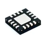
• RoHS Compliant 4×4-mm QFN-16 Package
• 2-V to 3.6-V Operation
•
•
•
IEEE 802.15.4 and ZigBee® Systems
Wireless Consumer Systems
Wireless Audio Systems
Description
CC2591 is a cost-effective and high-performance RF front end for low-power and low-voltage 2.4-GHz
wireless applications. The device is a range extender for all existing and future 2.4-GHz low-power RF
transceivers, transmitters, and System-on-Chip products from TI. CC2591 increases the link budget by
providing a power amplifier for increased output power, and an LNA with low noise figure for improved
receiver sensitivity. The device provides a small size, high output power RF design with its 4-mm × 4-mm
QFN-16 package. The device contains PA, LNA, switches, RF-matching, and balun for simple design of
high-performance wireless applications.
Device Information (1)
PART NUMBER
CC2591RGV
(1)
PACKAGE
BODY SIZE
RGV (16)
4.00 mm × 4.00 mm
For more information, see Section 7, Mechanical Packaging and Orderable Information.
1
An IMPORTANT NOTICE at the end of this data sheet addresses availability, warranty, changes, use in safety-critical applications,
intellectual property matters and other important disclaimers. PRODUCTION DATA.
�CC2591
SWRS070B – MARCH 2008 – REVISED SEPTEMBER 2014
1.4
www.ti.com
Functional Block Diagram
Figure 1-1 shows the functional block diagram of the device.
PA
BALUN
4
RF_P
3
RXTX
2
RF_N
5
PAEN
6
EN
11
ANT
LNA
Logic
Bias
15
7
BIAS
HGM
Figure 1-1. Functional Block Diagram
2
Device Overview
Copyright © 2008–2014, Texas Instruments Incorporated
Submit Documentation Feedback
Product Folder Links: CC2591
�CC2591
www.ti.com
SWRS070B – MARCH 2008 – REVISED SEPTEMBER 2014
Table of Contents
1
2
3
Device Overview ......................................... 1
Typical Characteristics
...............................
8
Features .............................................. 1
1.2
Applications ........................................... 1
5.1
CC2591EM Evaluation Module ....................... 9
1.3
Description ............................................ 1
5.2
Controlling the Output Power from CC2591
1.4
Functional Block Diagram ............................ 2
5
6
Applications, Implementation, and Layout ......... 9
........
10
Device and Documentation Support ............... 14
Revision History ......................................... 3
Terminal Configuration and Functions .............. 4
6.1
Device Support ...................................... 14
6.2
Documentation Support ............................. 15
Pin Attributes ......................................... 5
6.3
Trademarks.......................................... 15
............................................
Absolute Maximum Ratings ..........................
Handling Ratings .....................................
Recommended Operating Conditions ................
Electrical Characteristics .............................
3.1
4
4.6
1.1
Specifications
6
6.4
Electrostatic Discharge Caution ..................... 16
4.1
6
6.5
Export Control Notice
4.2
4.3
4.4
4.5
6
6
6
Thermal Resistance Characteristics for RGV
Package .............................................. 7
6.6
7
...............................
Glossary .............................................
16
16
Mechanical Packaging and Orderable
Information .............................................. 17
7.1
Packaging Information
..............................
17
2 Revision History
NOTE: Page numbers for previous revisions may differ from page numbers in the current version.
Changes from Revision A (June 2008) to Revision B
•
Page
Changed format of data sheet to the latest TI standards........................................................................ 1
Revision History
Copyright © 2008–2014, Texas Instruments Incorporated
Submit Documentation Feedback
Product Folder Links: CC2591
3
�CC2591
SWRS070B – MARCH 2008 – REVISED SEPTEMBER 2014
www.ti.com
3 Terminal Configuration and Functions
15
14
AVDD_LNA
BIAS
16
GND
AVDD_BIAS
The CC2591 pinout and description are shown in Figure 3-1 and Table 3-1, respectively.
13
AVDD_PA1
1
12
GND
RF_N
2
11
ANT
RXTX
3
10
AVDD_PA2
RF_P
4
9
EN
7
8
GND
6
HGM
5
PAEN
QFN-16 4x4mm
GND
Figure 3-1. PIN AND I/O CONFIGURATION (TOP VIEW)
NOTE
The exposed die attach pad must be connected to a solid ground plane as this is the
primary ground connection for the chip. Inductance in vias to the pad should be minimized. It
is highly recommended to follow the reference layout. Changes will alter the performance.
For best performance, minimize the length of the ground vias, by using a 4-layer PCB with
ground plane as layer 2 when CC2591 is mounted onto layer 1.
4
Terminal Configuration and Functions
Copyright © 2008–2014, Texas Instruments Incorporated
Submit Documentation Feedback
Product Folder Links: CC2591
�CC2591
www.ti.com
3.1
SWRS070B – MARCH 2008 – REVISED SEPTEMBER 2014
Pin Attributes
Table 3-1. Pin Attributes
TERMINAL
TYPE
DESCRIPTION
NO.
NAME
—
GND
Ground
The exposed die attach pad must be connected to a solid ground plane. See
CC2591EM reference design for recommended layout.
AVDD_PA1
Power
2.0 V – 3.6 V Power. PCB trace to this pin serves as inductive load to PA . See
CC2591EM reference design for recommended layout.
2
RF_N
RF
3
RXTX
Analog/Control
1
RF interface towards CC24xx or CC25xx device.
RXTX switching voltage when connected to CC24xx devices. See Table 5-2 and
Table 5-3 for details.
4
RF_P
RF
5
PAEN
Digital Input
RF interface towards CC24xx or CC25xx device
Digital control pin. See Table 5-2 and Table 5-3 for details.
6
EN
Digital Input
Digital control pin. See Table 5-2 and Table 5-3 for details.
7
HGM
Digital Input
Digital control pin.
HGM=1 → Device in High Gain Mode
HGM=0 → Device in Low Gain Mode (RX only)
8, 9, 12, 14
GND
Ground
Secondary ground connections. Should be shorted to the die attach pad on the top
PCB layer.
10
AVDD_PA2
Power
2.0 V – 3.6 V Power. PCB trace to this pin serves as inductive load to PA. See
CC2591EM reference design for recommended layout.
11
ANT
RF
13
AVDD_LNA
Power
2 V – 3.6 V Power. PCB trace to this pin serves as inductive load to LNA. See
CC2591EM reference design for recommended layout.
15
BIAS
Analog
Biasing input. Resistor between this node and ground sets bias current to PAs.
16
AVDD_BIAS
Power
2 V – 3.6 V Power.
Antenna interface.
Terminal Configuration and Functions
Copyright © 2008–2014, Texas Instruments Incorporated
Submit Documentation Feedback
Product Folder Links: CC2591
5
�CC2591
SWRS070B – MARCH 2008 – REVISED SEPTEMBER 2014
www.ti.com
4 Specifications
Absolute Maximum Ratings (1) (2)
4.1
Under no circumstances must the absolute maximum ratings be violated. Stress exceeding one or more of the limiting values
may cause permanent damage to the device.
PARAMETER
Supply voltage
VALUE
All supply pins must have the same voltage
Voltage on any digital pin
(2)
dBm
Handling Ratings
Tstg
MIN
MAX
UNIT
–50
150
°C
Human Body Model (HBM), per ANSI/ESDA/JEDEC
JS001 (1)
–600
600
V
Charged Device Model (CDM),
per JESD22-C101 (2)
–500
500
V
Storage temperature range
Electrostatic discharge (ESD)
performance:
VESD
4.3
10
Stresses beyond those listed under absolute maximum ratings may cause permanent damage to the device. These are stress ratings
only, and functional operation of the device at these or any other conditions beyond those indicated under recommended operating
conditions is not implied. Exposure to absolute-maximum-rated conditions for extended periods may affect device reliability.
All voltage values are with respect to VSS, unless otherwise noted.
4.2
(1)
(2)
V
–0.3 to VDD + 0.3, max 3.6
Input RF level
(1)
UNIT
–0.3 to 3.6
JEDEC document JEP155 states that 500-V HBM allows safe manufacturing with a standard ESD control process.
JEDEC document JEP157 states that 250-V CDM allows safe manufacturing with a standard ESD control process.
Recommended Operating Conditions
The operating conditions for CC2591 are listed below.
PARAMETER
Ambient temperature range
MIN
MAX
–40
85
°C
2
3.6
V
2400
2483.5
Operating supply voltage
Operating frequency range
4.4
UNIT
MHz
Electrical Characteristics
TC = 25°C, VDD = 3 V , fRF= 2440 MHz (unless otherwise noted). Measured on CC2591EM reference design including external
matching components.
PARAMETER
TEST CONDITIONS
MIN
TYP
MAX
Receive current, High-Gain Mode
HGM = 1
3.4
4
Receive current, Low-Gain Mode
HGM = 0
1.7
2
Transmit current
PIN = 0.5 dBm
112
Transmit current
No input signal
40
50
Power-down current
EN = PAEN = 0
0.1
0.3
High-input level (control pins)
EN, PAEN, HGM, RXTX
Low-input level (control pins)
EN, PAEN, HGM, RXTX
1.3
VDD
0.3
UNIT
mA
μA
V
Power down - Receive mode switching
time
12
μs
Power down - Transmit mode switching
time
1
μs
RF Receive
Gain, High-Gain Mode
HGM = 1
11
dB
Gain, Low-Gain Mode
HGM = 0
1
dB
Gain variation, 2400 – 2483.5 MHz, HighGain Mode
HGM = 1
1.3
dB
Gain variation, 2.0 V – 3.6 V, High-Gain
Mode
HGM = 1
1.5
dB
6
Specifications
Copyright © 2008–2014, Texas Instruments Incorporated
Submit Documentation Feedback
Product Folder Links: CC2591
�CC2591
www.ti.com
SWRS070B – MARCH 2008 – REVISED SEPTEMBER 2014
Electrical Characteristics (continued)
TC = 25°C, VDD = 3 V , fRF= 2440 MHz (unless otherwise noted). Measured on CC2591EM reference design including external
matching components.
PARAMETER
TEST CONDITIONS
Gain variation, -40°C – 85°C, High-Gain
Mode
HGM = 1
Noise figure, High-Gain Mode
MIN
TYP
MAX
UNIT
3
dB
HGM = 1, including internal T/R switch and external
antenna match
4.8
dB
Input 1-dB compression, High-Gain Mode
HGM = 1
–17
dBm
Input IP3, High-Gain Mode
HGM = 1
–2
dBm
Input reflection coefficient, S11
HGM = 1, measured at antenna port
–11
dB
Output power, POUT
PIN = 0.5 dBm
20.6
dBm
Maximum output power
PIN = 5 dBm
22
dBm
Power Added Efficiency, PAE
PIN = 0.5 dBm
RF Transmit
Gain
22
dB
34%
Output 1-dB compression
Output IP3
19
dBm
32
dBm
Output power variation over frequency
2400 – 2483.5 MHz, PIN = 0.5 dBm
0.5
dB
Output power variation over power supply
2 V – 3.6 V , PIN = 0.5 dBm
3.5
dB
Output power variation over temperature
-40°C – 85°C, PIN = 0.5 dBm
1.5
dB
Second harmonic power
PIN = 0.5 dBm. The second harmonic can be reduced
to below regulatory limits by using an external LC filter
and antenna.
–15
dBm
Third harmonic power
PIN = 0.5 dBm. The third harmonic can be reduced to
below regulatory limits by using an external LC filter
and antenna.
–30
dBm
4.5
Thermal Resistance Characteristics for RGV Package
°C/W (1)
(2)
AIR FLOW (m/s) (3)
NAME
DESCRIPTION
RΘJC-top
Junction-to-case (top)
52.8
0.00
RΘJB
Junction-to-board
20.4
0.00
RΘJA
Junction-to-free air
41.9
0.00
PsiJT
Junction-to-package top
1.4
0.00
PsiJB
Junction-to-board
20.5
0.00
RΘJC-bottom
Junction-to-case (bottom)
8.3
0.00
(1)
(2)
(3)
°C/W = degrees Celsius per watt.
These values are based on a JEDEC-defined 2S2P system (with the exception of the Theta JC [RΘJC] value, which is based on a
JEDEC-defined 1S0P system) and will change based on environment as well as application. For more information, see these
EIA/JEDEC standards:
• JESD51-2, Integrated Circuits Thermal Test Method Environmental Conditions - Natural Convection (Still Air)
• JESD51-3, Low Effective Thermal Conductivity Test Board for Leaded Surface Mount Packages
• JESD51-7, High Effective Thermal Conductivity Test Board for Leaded Surface Mount Packages
• JESD51-9, Test Boards for Area Array Surface Mount Package Thermal Measurements
m/s = meters per second.
Specifications
Copyright © 2008–2014, Texas Instruments Incorporated
Submit Documentation Feedback
Product Folder Links: CC2591
7
�CC2591
SWRS070B – MARCH 2008 – REVISED SEPTEMBER 2014
4.6
Typical Characteristics
12
5.4
13
11
5.3
12
HGM
11
5.2
5.1
8
5
4.9
7
NF HGM
6
4.8
5
4.7
4
4.6
3
4.5
2
9
8
Gain − dB
9
7
6
5
4
3
1
0
1
4.3
-1
0
4.2
-2
-40
2400 2410
2420
2430 2440 2450
2460
2470
LGM
2
4.4
LGM
HGM
10
Noise Figure − dB
10
Gain − dB
www.ti.com
2480
-20
0
20
40
60
80
o
T − Temperature − C
Figure 4-2. LNA Gain vs Temperature
f − Frequency − MHz
Figure 4-1. LNA Gain and Noise Figure vs Frequency
12
11
10
HGM
9
Gain − dB
8
7
6
5
4
3
2
LGM
1
0
-1
2
2.2
2.4
2.6
2.8
3
3.2
3.4
3.6
Power Supply − V
Figure 4-3. LNA Gain vs Power Supply
8
Specifications
Copyright © 2008–2014, Texas Instruments Incorporated
Submit Documentation Feedback
Product Folder Links: CC2591
�CC2591
www.ti.com
SWRS070B – MARCH 2008 – REVISED SEPTEMBER 2014
5 Applications, Implementation, and Layout
NOTE
Information in the following applications sections is not part of the TI component
specification, and TI does not warrant its accuracy or completeness. TI’s customers are
responsible for determining suitability of components for their purposes. Customers should
validate and test their design implementation to confirm system functionality.
5.1
CC2591EM Evaluation Module
VDD VDD
C11/C12
C101/C102
= TLINE inductor
VDD
VDD
C131/C132
TL131
AVDD_LNA
TL101
AVDD_PA2
AVDD_BIAS
AVDD_PA1
TL11
C161
LDB182G4520C-110
RF_P
RXTX
RXTX
RXTX
SMA
L111
L112
CC2591
ANT
C111
Balun
C2
RF_N
RF_N
RF_N
PAEN
PAEN
EN
EN
HGM
HGM
BIAS
SMA
RF_P
RF_P
RXTX
R151
Figure 5-1. CC2591EM Evaluation Module
Applications, Implementation, and Layout
Copyright © 2008–2014, Texas Instruments Incorporated
Submit Documentation Feedback
Product Folder Links: CC2591
9
�CC2591
SWRS070B – MARCH 2008 – REVISED SEPTEMBER 2014
www.ti.com
Table 5-1. List of Materials (See CC2591EM Reference Design)
DEVICE
FUNCTION
VALUE
L112
Part of antenna match.
1.5 nH: LQW15AN1N5B00 from Murata
L111
DC block.
1 nF: GRM1555C1H102JA01 from Murata
C111
Part of antenna match.
1 pF: GRM1555C1H1R0BZ01 from Murata
C161
Decoupling capacitor.
1 nF: GRM1555C1H102JA01 from Murata
C11/C12
Decoupling. Will affect PA resonance.
10 pF || 1 nF. The smallest cap closest. See CC2591EM
reference design (SWRU190) for placement.
10 pF: GRM1555C1H100JZ01 from Murata
1 nF: GRM1555C1H102JA01 from Murata
C101/C102
Decoupling. Will affect PA resonance.
18 pF || 1 nF. The smallest cap closest. See CC2591EM
reference design (SWRU190) for placement.
18 pF: GRM1555C1H180JZ01 from Murata
1 nF: GRM1555C1H102JA01 from Murata
C131/C132
Decoupling. Will affect PA resonance.
10 pF || 1 nF. The smallest cap closest. See CC2591EM
reference design (SWRU190) for placement.
10 pF: GRM1555C1H100JZ01 from Murata
1 nF: GRM1555C1H102JA01 from Murata
C2
Decoupling of external balun
1 nF: GRM1555C1H102JA01 from Murata
TL11
Transmission line. Will affect PA resonance.
See CC2591EM reference design.
TL101
Transmission line. Will affect PA resonance.
See CC2591EM reference design.
TL131
Transmission line. Will affect LNA resonance.
See CC2591EM reference design.
R151
Bias resistor
4.3 kΩ: RK73H1ETTP4301F from Koa
5.2
Controlling the Output Power from CC2591
The output power of CC2591 is controlled by controlling the input power. The CC2591 PA is designed to
work in compression (class AB), and the best efficiency is reached when a strong input signal is applied.
5.2.1
Input Levels on Control Pins
The four digital control pins (PAEN, EN, HGM, RXTX) have built-in level-shifting functionality, meaning
that if the CC2591 is operating from a 3.6-V supply voltage, the control pins will still sense 1.6-V - 1.8-V
signals as logical ‘1’.
An example of the above would be that RXTX is connected directly to the RXTX pin on CC24xx, but the
global supply voltage is 3.6 V. The RXTX pin on CC24xx will switch between 0 V (RX) and 1.8 V(TX),
which is still a high enough voltage to control the mode of CC2591.
The input voltages should however not have logical ‘1’ level that is higher than the supply.
5.2.2
Connecting CC2591 to a CC24xx Device
Table 5-2. Control Logic for Connecting CC2591 to a CC24xx Device
10
PAEN = EN
RXTX
HGM
0
X
X
Power Down
1
0
0
RX Low Gain Mode
1
0
1
RX High Gain Mode
1
1
X
TX
Applications, Implementation, and Layout
MODE OF OPERATION
Copyright © 2008–2014, Texas Instruments Incorporated
Submit Documentation Feedback
Product Folder Links: CC2591
�CC2591
www.ti.com
SWRS070B – MARCH 2008 – REVISED SEPTEMBER 2014
VDD VDD
C11/C12
C101/C102
= TLINE inductor
VDD
VDD
C131/C132
TL131
AVDD_LNA
TL101
AVDD_PA2
AVDD_BIAS
AVDD_PA1
TL11
C161
CC243x
RF_P
RF_P
RF_P
RF_P
RXTX
RXTX
RXTX
L111
ANT
L112
C113
TXRX_SWITCH
C112
CC2591
RF_N
RF_N
RF_N
RF_N
PAEN
C111
RREG_OUT (CC243x)
BIAS
EN
HGM
R151
Connected to
VDD/GND/MCU/RXTX
Alternativiely
from MCU
Figure 5-2. CC2591 + CC24xx Application Circuit
Applications, Implementation, and Layout
Copyright © 2008–2014, Texas Instruments Incorporated
Submit Documentation Feedback
Product Folder Links: CC2591
11
�CC2591
SWRS070B – MARCH 2008 – REVISED SEPTEMBER 2014
5.2.3
www.ti.com
Connecting CC2591 to the CC2500, CC2510, or CC2511 Device
Table 5-3. Control Logic for Connecting CC2591 to a CC2500/10/11 Devices
PAEN
EN
RXTX
HGM
MODE OF OPERATION
0
0
NC
X
Power Down
0
1
NC
0
RX LGM
0
1
NC
1
RX HGM
1
0
NC
X
TX
1
1
NC
X
Not allowed
VDD VDD
C11/C12
C101/C102
= TLINE inductor
VDD
VDD
C131/C132
TL131
AVDD_LNA
TL101
AVDD_PA2
AVDD_BIAS
AVDD_PA1
TL11
C161
CC2500
CC2510
CC2511
RF_P
RF_P
RF_P
RXTX
RXTX
RXTX
L111
CC2591
C111
BIAS
C113
NC
C112
ANT
L112
RF_P
RF_N
RF_N
RF_N
RF_N
PAEN
GDO0
EN
GDO2
HGM
R151
Connected to
VDD/GND/MCU
Alternatively
from MCU
Figure 5-3. CC2591 + CC2500/10/11 Device Application Circuit
12
Applications, Implementation, and Layout
Copyright © 2008–2014, Texas Instruments Incorporated
Submit Documentation Feedback
Product Folder Links: CC2591
�CC2591
www.ti.com
5.2.4
SWRS070B – MARCH 2008 – REVISED SEPTEMBER 2014
Connecting CC2591 to a CC2520 Device
Table 5-4. Control Logic for Connecting CC2591 to a CC2520 Device
PAEN
EN
RXTX
HGM
MODE OF OPERATION
0
0
NC
X
Power Down
0
1
NC
0
RX LGM
0
1
NC
1
RX HGM
1
0
NC
X
TX
1
1
NC
X
Not allowed
VDD VDD
C11/C12
C101/C102
= TLINE inductor
VDD
VDD
C131/C132
TL131
AVDD_LNA
TL101
AVDD_PA2
AVDD_BIAS
AVDD_PA1
TL11
C161
CC2520
C41
RF_P
RF_P
RXTX
C112
CC2591
ANT
L112
C113
C111
RF_P
RF_P
RXTX
RXTX
L111
L41
NC
C1
L21
RF_N
RF_N
RF_N
RF_N
PAEN
PA_EN
LNA_EN
BIAS
EN
HGM
R151
Connected to
VDD/GND/MCU
C21
Alternatively
from MCU
Figure 5-4. CC2591 + CC2520 Application Circuit
Applications, Implementation, and Layout
Copyright © 2008–2014, Texas Instruments Incorporated
Submit Documentation Feedback
Product Folder Links: CC2591
13
�CC2591
SWRS070B – MARCH 2008 – REVISED SEPTEMBER 2014
www.ti.com
6 Device and Documentation Support
6.1
6.1.1
Device Support
Development Support
TI offers an extensive line of development tools, including tools to evaluate the performance of the
processors, generate code, develop algorithm implementations, and fully integrate and debug software
and hardware modules. The tool's support documentation is electronically available within the Code
Composer Studio™ Integrated Development Environment (IDE).
The following products support development of the CC2591 device applications:
Software Development Tools: Code Composer Studio™ Integrated Development Environment (IDE):
including Editor C/C++/Assembly Code Generation, and Debug plus additional development tools
Scalable, Real-Time Foundation Software (DSP/BIOS™), which provides the basic run-time target
software needed to support any CC2591 device application.
Hardware Development Tools: Extended Development System (XDS™) Emulator
For a complete listing of development-support tools for the CC2591 platform, visit the Texas Instruments
website at www.ti.com. For information on pricing and availability, contact the nearest TI field sales office
or authorized distributor.
6.1.2
Device Nomenclature
To designate the stages in the product development cycle, TI assigns prefixes to the part numbers of all
microprocessors (MPUs) and support tools. Each device has one of three prefixes: X, P, or null (no prefix)
(for example, CC2591). These prefixes represent evolutionary stages of product development from
engineering prototypes (TMDX) through fully qualified production devices and tools (TMDS).
Device development evolutionary flow:
X
Experimental device that is not necessarily representative of the final device's electrical
specifications and may not use production assembly flow.
P
Prototype device that is not necessarily the final silicon die and may not necessarily meet
final electrical specifications.
null
Production version of the silicon die that is fully qualified.
Support tool development evolutionary flow:
X and P devices are shipped against the following disclaimer:
"Developmental product is intended for internal evaluation purposes."
Production devices have been characterized fully, and the quality and reliability of the device have been
demonstrated fully. TI's standard warranty applies.
Predictions show that prototype devices (X or P) have a greater failure rate than the standard production
devices. Texas Instruments recommends that these devices not be used in any production system
because their expected end-use failure rate still is undefined. Only qualified production devices are to be
used.
TI device nomenclature also includes a suffix with the device family name. This suffix indicates the
package type (for example, RGV) and the temperature range (for example, blank is the default
commercial temperature range). provides a legend for reading the complete device name for any CC2591
device.
For orderable part numbers of CC2591 devices in the RGV package types, see the Package Option
Addendum of this document, the TI website (www.ti.com), or contact your TI sales representative.
14
Device and Documentation Support
Copyright © 2008–2014, Texas Instruments Incorporated
Submit Documentation Feedback
Product Folder Links: CC2591
�CC2591
www.ti.com
6.2
SWRS070B – MARCH 2008 – REVISED SEPTEMBER 2014
Documentation Support
The following documents describe the CC2591 processor. Copies of these documents are available on the
Internet at www.ti.com.
6.2.1
SWRA351
Antenna Quick Guide
SWRA120
Design Note Overview
SWRA350
YAGI 2.4 GHz PCB Antenna
SWRA161
Antenna Selection Guide
SWRA328
CC-Antenna-DK Documentation and Antenna Measurements Summary
SWRA229
Using CC2591 RF Front End with CC2520
SWRA308
Using CC2591 Front End with CC2530 and CC2531
SWRA290
TIMAC and Z-Stack Modifications for using CC2591 RF Front End with CC2
SWRA236
Design Steps and Results for Changing PCB Layer Thickness
SWRA230
TI-MAC modifications for using CC2591 PA/LNA with MSP430F2618+CC2520
SWRA208
TI-MAC and Z-Stack modifications for using CC2591 RF Front End w/CC2430
SWRA212
Using CC2591 RF Front End with CC2430
SWRC171
CC2530-CC2591EM Reference Design
SPRU137
CC2520 Software Examples User's Guide
SPRU178
CC2430 Software Examples User’s Guide
Community Resources
The following links connect to TI community resources. Linked contents are provided "AS IS" by the
respective contributors. They do not constitute TI specifications and do not necessarily reflect TI's views;
see TI's Terms of Use.
TI E2E™ Online Community TI's Engineer-to-Engineer (E2E) Community. Created to foster
collaboration among engineers. At e2e.ti.com, you can ask questions, share knowledge,
explore ideas and help solve problems with fellow engineers.
TI Embedded Processors Wiki Texas Instruments Embedded Processors Wiki. Established to help
developers get started with Embedded Processors from Texas Instruments and to foster
innovation and growth of general knowledge about the hardware and software surrounding
these devices.
6.3
Trademarks
E2E is a trademark of Texas Instruments.
ZigBee is a registered trademark of ZigBee Alliance.
Device and Documentation Support
Copyright © 2008–2014, Texas Instruments Incorporated
Submit Documentation Feedback
Product Folder Links: CC2591
15
�CC2591
SWRS070B – MARCH 2008 – REVISED SEPTEMBER 2014
6.4
www.ti.com
Electrostatic Discharge Caution
This integrated circuit can be damaged by ESD. Texas Instruments recommends that all integrated circuits be handled with
appropriate precautions. Failure to observe proper handling and installation procedures can cause damage.
ESD damage can range from subtle performance degradation to complete device failure. Precision integrated circuits may be more
susceptible to damage because very small parametric changes could cause the device not to meet its published specifications.
6.5
Export Control Notice
Recipient agrees to not knowingly export or re-export, directly or indirectly, any product or technical data
(as defined by the U.S., EU, and other Export Administration Regulations) including software, or any
controlled product restricted by other applicable national regulations, received from disclosing party under
nondisclosure obligations (if any), or any direct product of such technology, to any destination to which
such export or re-export is restricted or prohibited by U.S. or other applicable laws, without obtaining prior
authorization from U.S. Department of Commerce and other competent Government authorities to the
extent required by those laws.
6.6
Glossary
SLYZ022 — TI Glossary.
This glossary lists and explains terms, acronyms, and definitions.
16
Device and Documentation Support
Copyright © 2008–2014, Texas Instruments Incorporated
Submit Documentation Feedback
Product Folder Links: CC2591
�CC2591
www.ti.com
SWRS070B – MARCH 2008 – REVISED SEPTEMBER 2014
7 Mechanical Packaging and Orderable Information
7.1
Packaging Information
The following pages include mechanical packaging and orderable information. This information is the most
current data available for the designated devices. This data is subject to change without notice and
revision of this document. For browser-based versions of this data sheet, refer to the left-hand navigation.
Copyright © 2008–2014, Texas Instruments Incorporated
Mechanical Packaging and Orderable Information
Submit Documentation Feedback
Product Folder Links: CC2591
17
�PACKAGE OPTION ADDENDUM
www.ti.com
19-Oct-2022
PACKAGING INFORMATION
Orderable Device
Status
(1)
Package Type Package Pins Package
Drawing
Qty
Eco Plan
(2)
Lead finish/
Ball material
MSL Peak Temp
Op Temp (°C)
Device Marking
(3)
(4/5)
(6)
CC2591RGVR
NRND
VQFN
RGV
16
2500
RoHS & Green
NIPDAU
Level-2-260C-1 YEAR
-40 to 85
CC2591
CC2591RGVT
NRND
VQFN
RGV
16
250
RoHS & Green
NIPDAU
Level-2-260C-1 YEAR
-40 to 85
CC2591
CC2591RGVTG4
NRND
VQFN
RGV
16
250
RoHS & Green
NIPDAU
Level-2-260C-1 YEAR
-40 to 85
CC2591
(1)
The marketing status values are defined as follows:
ACTIVE: Product device recommended for new designs.
LIFEBUY: TI has announced that the device will be discontinued, and a lifetime-buy period is in effect.
NRND: Not recommended for new designs. Device is in production to support existing customers, but TI does not recommend using this part in a new design.
PREVIEW: Device has been announced but is not in production. Samples may or may not be available.
OBSOLETE: TI has discontinued the production of the device.
(2)
RoHS: TI defines "RoHS" to mean semiconductor products that are compliant with the current EU RoHS requirements for all 10 RoHS substances, including the requirement that RoHS substance
do not exceed 0.1% by weight in homogeneous materials. Where designed to be soldered at high temperatures, "RoHS" products are suitable for use in specified lead-free processes. TI may
reference these types of products as "Pb-Free".
RoHS Exempt: TI defines "RoHS Exempt" to mean products that contain lead but are compliant with EU RoHS pursuant to a specific EU RoHS exemption.
Green: TI defines "Green" to mean the content of Chlorine (Cl) and Bromine (Br) based flame retardants meet JS709B low halogen requirements of