TI CC3000 BoosterPack Evaluation Module
Board
User's Guide
Literature Number: SWRU331A
November 2012 – Revised August 2014
�Contents
Preface ........................................................................................................................................ 4
Revision History ........................................................................................................................... 5
1
Introduction ......................................................................................................................... 6
2
CC3000 BoosterPack EVM Board ........................................................................................... 7
2.1
2.2
2.3
2.4
2.5
2.6
BoosterPack EVM Board Top View ....................................................................................... 7
CC3000 BoosterPack EVM Board Bottom View ......................................................................... 9
Antenna ...................................................................................................................... 10
Hardware Setup ............................................................................................................ 13
CC3000 BoosterPack Schematic ........................................................................................ 14
Bill of Materials (BOM) ..................................................................................................... 15
2.6.1 PCB Design Guidelines .......................................................................................... 15
2.6.2 RF Trace ........................................................................................................... 15
2.6.3 Antenna ............................................................................................................. 16
2.6.4 Power Trace ....................................................................................................... 17
2.6.5 Ground .............................................................................................................. 17
3
Application Development .................................................................................................... 18
2
Contents
SWRU331A – November 2012 – Revised August 2014
Submit Documentation Feedback
Copyright © 2012–2014, Texas Instruments Incorporated
�www.ti.com
List of Figures
.....................................................................................
2-1.
BoosterPack EVM Board (Top View)
2-2.
CC3000 BoosterPack EVM Board (Bottom View) ....................................................................... 9
2-3.
Antenna Location and RF Trace Routing ............................................................................... 10
2-4.
Matching Circuit Between the Antenna and the CC3000 BoosterPack EVM Board .............................. 11
2-5.
Return Loss From the ACX Antenna and Matching Circuit ........................................................... 11
2-6.
Antenna Radiation Pattern ................................................................................................ 12
2-7.
Host PCB Mating Connector Arrangement ............................................................................. 13
2-8.
CC3000 BoosterPack Schematics ....................................................................................... 14
2-9.
Trace Design for PCB Layout
2-10.
Antenna Layout Guidelines ............................................................................................... 16
2-11.
Power Trace
2-12.
Ground Routing for the CC3000 BoosterPack EVM Board ........................................................... 17
3-1.
MSP-EXP430G2 Test Platform and CC3000 BoosterPack EVM Board ............................................ 18
............................................................................................
................................................................................................................
7
15
17
List of Tables
2-1.
Key Parts of CC3000 BoosterPack EVM Board Top View ............................................................. 7
2-2.
J2 Configuration of the CC3000 EVM Board............................................................................. 8
2-3.
Header J11 of the CC3000 BoosterPack EVM Board Top View ...................................................... 8
2-4.
Header J12 of the CC3000 BoosterPack EVM Board Top View ...................................................... 8
2-5.
Header J9 of the CC3000 BoosterPack EVM Board (Bottom View) .................................................. 9
2-6.
Header J10 of the CC3000 BoosterPack EVM Board (Bottom View) ............................................... 10
2-7.
LaunchPad to BoosterPack Pin Comparison ........................................................................... 13
2-8.
PCB Stack-Up Data ........................................................................................................ 15
2-9.
Trace Design Measurement Values ..................................................................................... 16
SWRU331A – November 2012 – Revised August 2014
Submit Documentation Feedback
Copyright © 2012–2014, Texas Instruments Incorporated
List of Figures
3
�Preface
SWRU331A – November 2012 – Revised August 2014
Read This First
About This Manual
This user guide describes how to use the TI CC3000 BoosterPack evaluation module (EVM) board to
evaluate the performance of the TI CC3000 module.
Related Documentation From Texas Instruments
•
•
TI SimpleLink™ CC3000 Module – Wi-Fi 802.11b/g Network Processor Data Sheet (SWRS126)
CC3000 wiki
If You Need Assistance
The primary sources of CC3000 information are the device-specific data sheets and user’s guides. For the
most up-to-date version of the user’s guide and data sheets, see the CC3000 module product page.
FCC Warning
This equipment is intended for use in a laboratory test environment only. It generates, uses, and can
radiate radio frequency energy and has not been tested for compliance with the limits of computing
devices pursuant to subpart J of part 15 of FCC rules, which are designed to provide reasonable
protection against radio frequency interference. Operation of this equipment in other environments may
cause interference with radio communications, in which case the user at his own expense will be required
to take whatever measures may be required to correct this interference.
SimpleLink is a trademark of Texas Instruments.
Wi-Fi is a registered trademark of Wi-Fi Alliance.
4
Read This First
SWRU331A – November 2012 – Revised August 2014
Submit Documentation Feedback
Copyright © 2012–2014, Texas Instruments Incorporated
�Revision History
www.ti.com
Revision History
Changes from Original (November 2012) to A Revision ................................................................................................ Page
•
•
•
•
•
•
Changed wiki title in Related Documentation From Texas Instruments ........................................................... 4
Changed link name in If You Need Assistance ....................................................................................... 4
Changed wiki title in Table 2-2 .......................................................................................................... 8
Changed typo in Table 2-6: name for pin 7 changed from WL_SPI_CLK, pin type changed from input, and description
changed from clock input ............................................................................................................... 10
Changed wiki title in Chapter 3 ........................................................................................................ 18
Changed link name in Chapter 3 ...................................................................................................... 18
NOTE: Page numbers for previous revisions may differ from page numbers in the current version.
SWRU331A – November 2012 – Revised August 2014
Submit Documentation Feedback
Copyright © 2012–2014, Texas Instruments Incorporated
Revision History
5
�Chapter 1
SWRU331A – November 2012 – Revised August 2014
Introduction
This user's guide describes how to use the TI CC3000 BoosterPack EVM board to evaluate the
performance and functionality of the TI CC3000 module. The TI CC3000 module is a self-contained Wi-Fi®
solution that enables Internet connectivity for a wide variety of embedded applications. This document
details the key parts and features of the CC3000 BoosterPack EVM board along with the different options
available for the user and includes layout guidelines to assist in PCB development.
6
Introduction
SWRU331A – November 2012 – Revised August 2014
Submit Documentation Feedback
Copyright © 2012–2014, Texas Instruments Incorporated
�Chapter 2
SWRU331A – November 2012 – Revised August 2014
CC3000 BoosterPack EVM Board
2.1
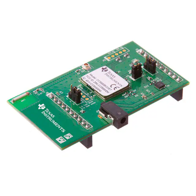
BoosterPack EVM Board Top View
Figure 2-1 shows the top view of the CC3000 BoosterPack EVM board.
SWRU331-001
Figure 2-1. BoosterPack EVM Board (Top View)
Table 2-1 describes the key parts and jumpers mounted on top of the CC3000 BoosterPack EVM board.
Table 2-1. Key Parts of CC3000 BoosterPack EVM Board Top View
Part Name
CC3000MOD
Antenna
Description
Core module for performance evaluation. For more information, see the CC3000 module
datasheet (SWRS126).
Can be used for radiated testing by reworking the capacitor to correct pads
J1
U.FL RF connector used for conductive power tests
J2
Used to swap between test mode and operation mode. When pins 2 and 3 are shorted, J2 runs in
operation mode. When pins 1 and 2 are shorted, J2 runs in test mode.
J11
Through-hole test points (for more information, see Table 2-3)
J12
Through-hole test points (for more information, see Table 2-4)
J13
Used to switch between external power and power from the motherboard. Can be used for power
measurements. Connect pins 1 and 2 for power from the LaunchPad flash programmer and
debugging tool. Connect pins 2 and 3 for external power.
J14
DC jack for external power supply. If power is not supplied from the motherboard, ensure that
external power is applied.
SWRU331A – November 2012 – Revised August 2014
Submit Documentation Feedback
Copyright © 2012–2014, Texas Instruments Incorporated
CC3000 BoosterPack EVM Board
7
�BoosterPack EVM Board Top View
www.ti.com
Table 2-2 describes the J2 configuration of the CC3000 EVM board.
Table 2-2. J2 Configuration of the CC3000 EVM Board
Mode
Description
Test mode: CC3000 radio
tool (1)
Connect pins 1 and 2. Test mode is used with the CC3000 radio tool to operate, test, and
calibrate the CC3000 chipset designs during development. This tool uses the RS232/UART pins
to run radio frequency (RF) RX and TX tests on the CC3000 module. For more information, see
the CC3000 wiki.
Functional mode: Normal mode Connect pins 2 and 3. Normal mode is for regular functionality between the host platform and the
CC3000 module.
(1)
For more information about test software for the PC, see the CC3000 wiki.
Table 2-3 describes the signals on J11.
Table 2-3. Header J11 of the CC3000 BoosterPack EVM Board Top View
Pin
Pin Name
Pin Type
Descriptions
1
Reserved
–
Reserved
2
Reserved
–
Reserved
3
WL_RS232_TX
Output
RS232 transmit output; used for radio tool serial interface
in test mode. Leave floating in functional mode.
4
WL_RS232_RX
Input
RS232 receive output; used for radio tool serial interface
in test mode. Leave floating in functional mode.
Table 2-4 describes the signals on J12.
Table 2-4. Header J12 of the CC3000 BoosterPack EVM Board Top View
8
Pin
Pin Name
Pin Type
1
GND
–
2
SCL_CC3000
Output
3
SCL__EEPROM
Input
I2C clock signal input from EEPROM inside the CC3000
module. This pin is connected to SCL_CC3000 using a
0-Ω resistor and is not used by end users.
4
SDA_CC3000
Input and output
I2C data signal from the CC3000 module. This pin is
connected to SDA_EEPROM using a 0-Ω resistor and is
not used by end users.
5
SDA_EEPROM
Input and output
I2C data signal from EEPROM inside the CC3000
module. This pin is connected to SDA_CC3000 using a
0-Ω resistor and is not used by end users.
CC3000 BoosterPack EVM Board
Descriptions
Ground
I2C clock signal output from the CC3000 module. This pin
is connected to SCL_EEPROM through a 0-Ω resistor
and is not used by end users.
SWRU331A – November 2012 – Revised August 2014
Submit Documentation Feedback
Copyright © 2012–2014, Texas Instruments Incorporated
�CC3000 BoosterPack EVM Board Bottom View
www.ti.com
2.2
CC3000 BoosterPack EVM Board Bottom View
The two BoosterPack mating connectors (J9 and J10) connect to the host platform and mount to the
bottom of the BoosterPack EVM board, as shown in Figure 2-2.
SWRU331-002
Figure 2-2. CC3000 BoosterPack EVM Board (Bottom View)
Table 2-5 describes the signals on J9.
Table 2-5. Header J9 of the CC3000 BoosterPack EVM Board (Bottom View)
Pin
Pin Name
Pin Type
Descriptions
1
VBAT_IN
Power In
2
VBAT_SW_EN
Input
3
Reserved
–
Reserved
4
Reserved
–
Reserved
5
Reserved
–
Reserved
6
Reserved
–
Reserved
7
WL_SPI_CLK
Input
8
Reserved
–
Reserved
9
Reserved
–
Reserved
10
Reserved
–
Reserved
Battery voltage input to module. For the MSP430 host
platform, VIO_HOST = VBAT_IN. For other platforms
that have different voltage levels from the battery
voltages, R14 can be removed.
Active-high enables signal from the host device
Host interface SPI clock input
SWRU331A – November 2012 – Revised August 2014
Submit Documentation Feedback
Copyright © 2012–2014, Texas Instruments Incorporated
CC3000 BoosterPack EVM Board
9
�Antenna
www.ti.com
Table 2-6 describes the signals on J10.
Table 2-6. Header J10 of the CC3000 BoosterPack EVM Board (Bottom View)
2.3
Pin
Pin Name
Pin Type
1
GND
–
Descriptions
2
WL_SPI_IRQ
Output
3
WL_SPI_CS
Input
4
Reserved
–
Reserved
5
Reserved
–
Reserved
6
WL_SPI_DIN
Input
7
WL_SPI_DOUT
Output
8
Reserved
–
Reserved
9
Reserved
–
Reserved
10
Reserved
–
Reserved
Ground
Host interface SPI interrupt request
Host interface SPI chip select
Host interface SPI data input
Host interface SPI data output
Antenna
The ACX ceramic mounts on the BoosterPack EVM board with a specific layout and matching circuit for
the radiation tests conducted in FCC, CE, and IC certifications. Figure 2-3 shows the location of the ACX
ceramic antenna on the BoosterPack EVM board and the RF trace routing from the CC3000 module to the
antenna.
AT8010-E2R9HAA
Z
X
Y
SWRU331-003
Figure 2-3. Antenna Location and RF Trace Routing
10
CC3000 BoosterPack EVM Board
SWRU331A – November 2012 – Revised August 2014
Submit Documentation Feedback
Copyright © 2012–2014, Texas Instruments Incorporated
�Antenna
www.ti.com
Figure 2-4 shows the matching circuit between the antenna and the BoosterPack EVM board.
AT8010-E2R9HAA
1.8 nH
1.5 pF
Figure 2-4. Matching Circuit Between the Antenna and the CC3000 BoosterPack EVM Board
The return loss is based on the matching circuit and RF trace routing, as shown in Figure 2-5.
SWRU331-005
Figure 2-5. Return Loss From the ACX Antenna and Matching Circuit
SWRU331A – November 2012 – Revised August 2014
Submit Documentation Feedback
Copyright © 2012–2014, Texas Instruments Incorporated
CC3000 BoosterPack EVM Board
11
�Antenna
www.ti.com
Figure 2-6 shows the antenna radiation pattern.
SWRU331-006
Figure 2-6. Antenna Radiation Pattern
12
CC3000 BoosterPack EVM Board
SWRU331A – November 2012 – Revised August 2014
Submit Documentation Feedback
Copyright © 2012–2014, Texas Instruments Incorporated
�Hardware Setup
www.ti.com
2.4
Hardware Setup
To conduct performance tests, connect the BoosterPack EVM board to the host platform using the J9 and
J10 mating connectors or the J11 and J12 single-row headers. The J9 and J10 mating connectors must
line up as shown in Figure 2-7. The J11 and J12 single-row headers require the signals from the EVM
board mating connectors to be wired to the host platform.
SWRU331-007
Figure 2-7. Host PCB Mating Connector Arrangement
Table 2-7 compares the pins of the LaunchPad MSP-EXP430G2 board with the CC3000 BoosterPack
EVM board.
Table 2-7. LaunchPad to BoosterPack Pin Comparison
Pin
MSP430 Port
1
VCC
VBAT_IN
2
P1.0
VBAT_SW_EN
3
P1.1/TX
NC
4
1.2/RX
NC
5
P1.3
NC
6
P1.4
NC
7
P1.5
WL_SPI_CLK
8
P2.0
NC
9
P2.1
NC
10
P2.2
NC
11
P2.3
NC
12
P2.4
NC
13
P2.5
NC
14
P1.6
WL_SPI_DOUT
15
P1.7
WL_SPI_DIN
16
T/SBWT
NC
17
T/SBW
NC
18
2.6/XOUT
WL_SPI_CS
19
P2.7/XIN
WL_SPI_IRQ
20
GND
GND
SWRU331A – November 2012 – Revised August 2014
Submit Documentation Feedback
Copyright © 2012–2014, Texas Instruments Incorporated
CC3000 BoosterPack
CC3000 BoosterPack EVM Board
13
�J2
Pin2 and Pin3 short
Pin1 and Pin2 short
Function mode
Mode
2
Test mode
1
2
3
RES1005
RES1005
0R
RES1005
RES1005
WL_SPI_DIN
WL_SPI_CLK
0R
0R
0R
0R
R15
R19
R18
R17
R16
10
GND
GND
WL_RS232_RX
WL_EN1
WL_RS232_TX
WL_EN2
RESERVED_2
Copyright © 2012–2014, Texas Instruments Incorporated
J11
NL_HEADER 1x4
H-1x4_2MM
1
2
3
4
NS_UARTD
WL_UART_DBG
WL_RS232_TX
WL_RS232_RX
SCL_CC3000
SCL_EEPROM
SDA_CC300
SDA_EEPROM
J12
NL_HEADER 1x5
H-1x5_2MM
1
2
3
4
5
Header for Debug
RES1005
WL_SPI_IRQ
8
WL_RS232_RX
WL_SPI_DOUT
7
WL_EN1
WL_SPI_CS
6
WL_RS232_TX
9
5
4
WL_EN2
CC3000MOD
U1
19
20
21
22
23
24
25
26
27
28
0R RES1005
R20
C10
0.1uF
CAP1005
U2
IN
N/C
N/C
EN
OUT
N/C
NR/FB
GND
TPS73701DRB
8
7
6
5
1
2
3
4
LED1
SML-LX0603IW
LED1608
C11
1uF
CAP1005
R23
30K
RES1005
R22
52.3K
RES1005
VBAT_IN
1
2
3
4
5
6
7
8
9
10
WL_SPI_CLK
VBAT_SW_EN
VBAT_IN
C8
1uF
CAP1005
J13
HEADER 1x3
H-1x3_2MM
1
2
3
Power Supply Option:
1-2 => Supplied from Launch Pad
2-3 => External Plug-in
J10
F101-SGP-D030-10
H-1x10_2.54
Connect to LaunchPad J2
WL_SPI_DIN
WL_SPI_DOUT
WL_SPI_IRQ
WL_SPI_CS
1
2
3
4
5
6
7
8
9
10
SWRU331-008
Resistor Values for Output Voltages:
3.3V => R22=52.3K / R23=30K
3.6V => R22=56K / R23=28K
C12
NL
CAP1005
BoosterPack Connector
C9
10uF
CAP1608
J15
HEADER 1x2
H-1x2_2MM
R21
470R
RES1005
WL_VBAT
SDA_EEPROM
0R
RES1608
VBAT_SW_EN
Connect to LaunchPad J1
3
1
2
SCL_EEPROM
0R RES1608
VIO_HOST
0R RES1005
R2
J9
F101-SGP-D030-10
H-1x10_2.54
R13
R5
0R RES1608
Functional mode => R1,R2 - 0R to short I2C Pins
R1
SDA_CC300
SCL_CC3000
J14
3 PORT DC-JACK
DC-JACK-11.9x6x5-0.65
VBAT_IN
GND
EXT_32K
GND
VIO_HOST
RESERVED_3
GND
11
J2
HEADER 1x3
H-1x3_2MM
SDA_CC3000
VBAT_SW_EN
SDA_EEPROM
GND
WL_UART_DBG
NC
RESERVED_1
GND
12
3
SPI_CS
2
SPI_DOUT
13
1
C2
10pF
CAP1005
36
GND
C3
NL_10pF
CAP1005
35
RF_ANT
SPI_IRQ
14
NS_UARTD
2
1
3
34
GND
15
J1
NL_U.FL-R-SMT(10)
U.FL
33
GND
SPI_DIN
L2
2.2nH
IND1005
32
GND
16
L1
NL
IND1005
31
GND
GND
C1
2.2pF
CAP1005
30
SCL_CC3000
SPI_CLK
17
1
29
SCL_EEPROM
GND
18
ANT1
AT8010-E2R9HAA
AT8010
46
45
44
43
42
41
GND
GND
GND
GND
CC3000 BoosterPack EVM Board
37
38
39
40
14
1
2
2.5
GND
GND
GND
GND
GND
GND
CC3000MOD BoosterPack Board Schematic
CC3000 BoosterPack Schematic
www.ti.com
CC3000 BoosterPack Schematic
Figure 2-8 shows the CC3000 BoosterPack schematics.
Figure 2-8. CC3000 BoosterPack Schematics
SWRU331A – November 2012 – Revised August 2014
Submit Documentation Feedback
�Bill of Materials (BOM)
www.ti.com
2.6
Bill of Materials (BOM)
2.6.1 PCB Design Guidelines
The recommendations in this document are based on a two-layer PCB with the CC3000 module. The PCB
is built using standard FR4 material. Both layers are used for signal routing. TI recommends keeping the
traces of the SPI signals as short as possible. Table 2-8 shows the PCB stack-up data.
Table 2-8. PCB Stack-Up Data
PCB Stack Up
Layer
Type
Impedance
Thickness
Single end
Theory value
0.50 mil
copper + plating
1.82 mil
Trace 20 space 5,
50 Ω ±10%
47.57
Top side solder mask
L1
Top
Prepreg
52.20 mil
mil
L2
copper + plating
1.82 mil
mil
0.50 mil
56.84 mil
1.44 mm
Bottom side solder mask
TOTAL
2.6.2 RF Trace
Figure 2-9 shows a 50-Ω trace design recommended for the PCB layout.
SWRU331-009
Figure 2-9. Trace Design for PCB Layout
SWRU331A – November 2012 – Revised August 2014
Submit Documentation Feedback
Copyright © 2012–2014, Texas Instruments Incorporated
CC3000 BoosterPack EVM Board
15
�Bill of Materials (BOM)
www.ti.com
Table 2-9 lists the values associated with the trace design, including the measurements referenced in
Figure 2-9.
Table 2-9. Trace Design Measurement Values
Measurement
Length
H (height between L1 and L2)
52.2 mil
H1 (height 1)
0.5 mil
W (width)
19 mil
W1 (width 1)
20 mil
T (thickness)
1.82 mil
S (grid separation)
5 mil
εr (dielectric )
4.3
Zo (impedance)
47.57
2.6.3 Antenna
Figure 2-10 shows the specified guidelines for the BoosterPack antenna.
NOTE: The antenna vendor determines the antenna guidelines.
SWRU331-010
Figure 2-10. Antenna Layout Guidelines
16
CC3000 BoosterPack EVM Board
SWRU331A – November 2012 – Revised August 2014
Submit Documentation Feedback
Copyright © 2012–2014, Texas Instruments Incorporated
�Bill of Materials (BOM)
www.ti.com
2.6.4 Power Trace
Figure 2-11 shows the power trace for VBAT_IN highlighted in white.
NOTE: VBAT_IN must have a thickness of 24 mil or more.
SWRU331-011
Figure 2-11. Power Trace
2.6.5 Ground
The PCB must have a strong ground with more ground vias under the module for system stability and
thermal dissipation. Ground vias must be close to the pad.
Figure 2-12 shows the ground routing for the CC3000 BoosterPack EVM board.
SWRU331-012
Figure 2-12. Ground Routing for the CC3000 BoosterPack EVM Board
SWRU331A – November 2012 – Revised August 2014
Submit Documentation Feedback
Copyright © 2012–2014, Texas Instruments Incorporated
CC3000 BoosterPack EVM Board
17
�Chapter 3
SWRU331A – November 2012 – Revised August 2014
Application Development
TI supports the CC3000 BoosterPack paired with the TI MSP-EXP430G2 Launchpad, a microcontroller
(MCU) test platform.
The CC3000 BoosterPack lets users easily develop a complete Wi-Fi solution paired with the MSPEXP430G2 Launchpad platform.
For example applications, see the CC3000 wiki.
The CC3000 BoosterPack also can be used on other platforms with the same connector interface. The TI
wiki also has a host driver porting guide to assist with porting to other platforms.
Figure 3-1 shows the Launchpad MSP-EXP430G2 test platform and the CC3000 BoosterPack EVM
board.
SWRU331-013
Figure 3-1. MSP-EXP430G2 Test Platform and CC3000 BoosterPack EVM Board
To order the MSP-EXP430G2 test platform, see the MSP430 LaunchPad Value Line Development Kit.
18
Application Development
SWRU331A – November 2012 – Revised August 2014
Submit Documentation Feedback
Copyright © 2012–2014, Texas Instruments Incorporated
�IMPORTANT NOTICE
Texas Instruments Incorporated and its subsidiaries (TI) reserve the right to make corrections, enhancements, improvements and other
changes to its semiconductor products and services per JESD46, latest issue, and to discontinue any product or service per JESD48, latest
issue. Buyers should obtain the latest relevant information before placing orders and should verify that such information is current and
complete. All semiconductor products (also referred to herein as “components”) are sold subject to TI’s terms and conditions of sale
supplied at the time of order acknowledgment.
TI warrants performance of its components to the specifications applicable at the time of sale, in accordance with the warranty in TI’s terms
and conditions of sale of semiconductor products. Testing and other quality control techniques are used to the extent TI deems necessary
to support this warranty. Except where mandated by applicable law, testing of all parameters of each component is not necessarily
performed.
TI assumes no liability for applications assistance or the design of Buyers’ products. Buyers are responsible for their products and
applications using TI components. To minimize the risks associated with Buyers’ products and applications, Buyers should provide
adequate design and operating safeguards.
TI does not warrant or represent that any license, either express or implied, is granted under any patent right, copyright, mask work right, or
other intellectual property right relating to any combination, machine, or process in which TI components or services are used. Information
published by TI regarding third-party products or services does not constitute a license to use such products or services or a warranty or
endorsement thereof. Use of such information may require a license from a third party under the patents or other intellectual property of the
third party, or a license from TI under the patents or other intellectual property of TI.
Reproduction of significant portions of TI information in TI data books or data sheets is permissible only if reproduction is without alteration
and is accompanied by all associated warranties, conditions, limitations, and notices. TI is not responsible or liable for such altered
documentation. Information of third parties may be subject to additional restrictions.
Resale of TI components or services with statements different from or beyond the parameters stated by TI for that component or service
voids all express and any implied warranties for the associated TI component or service and is an unfair and deceptive business practice.
TI is not responsible or liable for any such statements.
Buyer acknowledges and agrees that it is solely responsible for compliance with all legal, regulatory and safety-related requirements
concerning its products, and any use of TI components in its applications, notwithstanding any applications-related information or support
that may be provided by TI. Buyer represents and agrees that it has all the necessary expertise to create and implement safeguards which
anticipate dangerous consequences of failures, monitor failures and their consequences, lessen the likelihood of failures that might cause
harm and take appropriate remedial actions. Buyer will fully indemnify TI and its representatives against any damages arising out of the use
of any TI components in safety-critical applications.
In some cases, TI components may be promoted specifically to facilitate safety-related applications. With such components, TI’s goal is to
help enable customers to design and create their own end-product solutions that meet applicable functional safety standards and
requirements. Nonetheless, such components are subject to these terms.
No TI components are authorized for use in FDA Class III (or similar life-critical medical equipment) unless authorized officers of the parties
have executed a special agreement specifically governing such use.
Only those TI components which TI has specifically designated as military grade or “enhanced plastic” are designed and intended for use in
military/aerospace applications or environments. Buyer acknowledges and agrees that any military or aerospace use of TI components
which have not been so designated is solely at the Buyer's risk, and that Buyer is solely responsible for compliance with all legal and
regulatory requirements in connection with such use.
TI has specifically designated certain components as meeting ISO/TS16949 requirements, mainly for automotive use. In any case of use of
non-designated products, TI will not be responsible for any failure to meet ISO/TS16949.
Products
Applications
Audio
www.ti.com/audio
Automotive and Transportation
www.ti.com/automotive
Amplifiers
amplifier.ti.com
Communications and Telecom
www.ti.com/communications
Data Converters
dataconverter.ti.com
Computers and Peripherals
www.ti.com/computers
DLP® Products
www.dlp.com
Consumer Electronics
www.ti.com/consumer-apps
DSP
dsp.ti.com
Energy and Lighting
www.ti.com/energy
Clocks and Timers
www.ti.com/clocks
Industrial
www.ti.com/industrial
Interface
interface.ti.com
Medical
www.ti.com/medical
Logic
logic.ti.com
Security
www.ti.com/security
Power Mgmt
power.ti.com
Space, Avionics and Defense
www.ti.com/space-avionics-defense
Microcontrollers
microcontroller.ti.com
Video and Imaging
www.ti.com/video
RFID
www.ti-rfid.com
OMAP Applications Processors
www.ti.com/omap
TI E2E Community
e2e.ti.com
Wireless Connectivity
www.ti.com/wirelessconnectivity
Mailing Address: Texas Instruments, Post Office Box 655303, Dallas, Texas 75265
Copyright © 2014, Texas Instruments Incorporated
�