Product
Folder
Sample &
Buy
Technical
Documents
Support &
Community
Tools &
Software
CDCE62002
SCAS882E – JUNE 2009 – REVISED OCTOBER 2016
CDCE62002 Four Output Clock Generator/Jitter Cleaner With Integrated Dual VCOs
1 Features
•
1
•
•
•
•
•
•
•
•
Frequency Synthesizer With PLL/VCO and
Partially Integrated Loop Filter
Fully Configurable Outputs Including Frequency
and Output Format
Smart Input Multiplexer Automatically Switches
Between One of Two Reference Inputs
Multiple Operational Modes Include Clock
Generation Through Crystal, SERDES Start-Up
Mode, Jitter Cleaning, and Oscillator Based
Holdover Mode
Integrated EEPROM Determines Device
Configuration at Power Up
Excellent Jitter Performance
Integrated Frequency Synthesizer Including PLL,
Multiple VCOs, and Loop Filter:
– Full Programmability Facilitates Phase Noise
Performance Optimization Enabling Jitter
Cleaner Mode
– Programmable Charge Pump Gain and Loop
Filter Settings
– Unique Dual-VCO Architecture Supports a
Wide Tuning Range 1.750 GHz to 2.356 GHz.
Universal Output Blocks Support Up to 2
Differential, 4 Single-Ended, or Combinations of
Differential or Single-Ended:
– 0.5 ps RMS (10 kHz to 20 MHz) Output Jitter
Performance
– Low Output Phase Noise: –130 dBc/Hz at
1 MHz Offset, Fc = 491.52 MHz
– Output Frequency Ranges From 10.94 MHz to
1.175 GHz in Synthesizer Mode
– LVPECL, LVDS, and LVCMOS
– Independent Output Dividers Support Divide
Ratios for 1, 2, 3, 4, 5, 8, 10, 12, 16, 20, 24,
and 32
Flexible Inputs With Innovative Smart Multiplexer:
– Two Universal Differential Inputs Accept
Frequencies from 1 MHz up to 500 MHz
(LVPECL), 500 MHz (LVDS), or 250 MHz
(LVCMOS)
– One Auxiliary Input Accepts Crystals in the
Range of 2 MHz to 42 MHz
– Clock Generator Mode Using Crystal Input
– Smart Input Multiplexer Can be Configured to
Automatically Switch Between Highest Priority
Clock Source Available Allowing for Fail-Safe
•
•
•
•
•
Operation
Typical Power Consumption 750 mW at 3.3 V
Integrated EEPROM Stores Default Settings;
Therefore, the Device Can Power Up in a Known,
Predefined State
Offered in QFN-32 Package
ESD Protection Exceeds 2000 V HBM
Industrial Temperature Range: –40°C to +85°C
2 Applications
•
•
•
•
•
•
•
Data Converter and Data Aggregation Clocking
Wireless Infrastructure
Switches and Routers
Medical Electronics
Military and Aerospace
Industrial
Clock Generation and Jitter Cleaning
3 Description
The CDCE62002 device is a high-performance clock
generator featuring low output jitter, a high degree of
configurability through a SPI interface, and
programmable start-up modes determined by on-chip
EEPROM. Specifically tailored for clocking data
converters and high-speed digital signals, the
CDCE62002 achieves jitter performance under 0.5 ps
RMS (1).
Device Information(1)
PART NUMBER
CDCE62002
PACKAGE
VQFN (32)
BODY SIZE (NOM)
5.00 mm × 5.00 mm
(1) For all available packages, see the orderable addendum at
the end of the data sheet.
CDCE62002 Application Example
Data
SERDES
Cleaned Clock
ASIC
ASIC Clock
Recovered Clock
CDCE62002
(1)
10-kHz to 20-MHz integration bandwidth.
1
An IMPORTANT NOTICE at the end of this data sheet addresses availability, warranty, changes, use in safety-critical applications,
intellectual property matters and other important disclaimers. PRODUCTION DATA.
�CDCE62002
SCAS882E – JUNE 2009 – REVISED OCTOBER 2016
www.ti.com
Table of Contents
1
2
3
4
5
6
7
Features ..................................................................
Applications ...........................................................
Description .............................................................
Revision History.....................................................
Description (continued).........................................
Pin Configuration and Functions .........................
Specifications.........................................................
7.1
7.2
7.3
7.4
7.5
7.6
8
9
1
1
1
2
5
5
7
Absolute Maximum Ratings ...................................... 7
Thermal Information .................................................. 7
Electrical Characteristics........................................... 7
Timing Requirements ................................................ 9
SPI Bus Timing Characteristics .............................. 10
Typical Characteristics ............................................ 11
Parameter Measurement Information ................ 12
Detailed Description ............................................ 13
9.1 Overview ................................................................. 13
9.2 Functional Block Diagrams ..................................... 13
9.3
9.4
9.5
9.6
Feature Description.................................................
Device Functional Modes........................................
Programming...........................................................
Register Maps .........................................................
17
31
33
36
10 Power Supply Recommendations ..................... 39
11 Layout................................................................... 40
11.1 Layout Guidelines ................................................. 40
11.2 Layout Example .................................................... 40
12 Device and Documentation Support ................. 41
12.1
12.2
12.3
12.4
12.5
Receiving Notification of Documentation Updates
Community Resources..........................................
Trademarks ...........................................................
Electrostatic Discharge Caution ............................
Glossary ................................................................
41
41
41
41
41
13 Mechanical, Packaging, and Orderable
Information ........................................................... 41
13.1 Package ................................................................ 41
4 Revision History
NOTE: Page numbers for previous revisions may differ from page numbers in the current version.
Changes from Revision D (February 2012) to Revision E
Page
•
Added figure cross references to Electrical Tables ................................................................................................................ 8
•
Added figure titles. ................................................................................................................................................................ 12
•
Updated Figure 18................................................................................................................................................................ 19
•
Updated Figure 20................................................................................................................................................................ 20
•
Corrected description for bits 0 and 1 in CDCE62002 Register 0 Bit Definitions ............................................................... 36
•
Corrected the register bits for LVPECL-AC, LVPECL-DC, LVDS-AC, LVDS-DC reference inputs in Reference Input
AC/DC Input Termination Table .......................................................................................................................................... 37
Changes from Revision C (March 2011) to Revision D
Page
•
Added 3 rows in TIMING REQUIREMENTS table, under Duty Cycle row ............................................................................ 9
•
Added a sentence below Equation 3.................................................................................................................................... 16
•
Changed last row last column in Figure 23 truth table from Disabled to Input Buffer Termination Disabled....................... 20
•
Changed in Table 13, second column, 5th and 6th row from 1 to 0 .................................................................................... 23
•
Added a reference to Table 11 and 2 references to Table 12 in Table 6 ............................................................................ 36
•
Added 6 crossreferences to Table 8 ................................................................................................................................... 37
•
Changed changed last row in Table 8 Description column, from "always reads 1" to "May read back to 1 or 0" ............... 37
Changes from Revision B (February 2010) to Revision C
Page
•
Changed the description of Pin 30, REF_IN-. ........................................................................................................................ 6
•
Changed Pin 7 to open drain in Pin Functions table .............................................................................................................. 6
•
Changed the description of Pin 19, TESTSYNC To: Reserved Pin.....resistor. ..................................................................... 6
•
Changed pin 31 From: Power To: A. Power in Pin Functions table....................................................................................... 6
•
Changed Pin Functions table, Pins 9, 12 to VCC_OUT0. Pins 13 and 16 to VCC_OUT1 .................................................... 6
•
Changed Note1 of the Pin Functions table............................................................................................................................. 6
2
Submit Documentation Feedback
Copyright © 2009–2016, Texas Instruments Incorporated
Product Folder Links: CDCE62002
�CDCE62002
www.ti.com
SCAS882E – JUNE 2009 – REVISED OCTOBER 2016
•
Deleted Dividers and from ELEC CHARACTERISTICS table in row POFF............................................................................. 7
•
Changed Crytal input section first row From: Crystal Load Capacitance To: On-chip Load Capacitance............................. 7
•
Added SPI OUTPUT row From: PLL To: PLL_LOCK ............................................................................................................ 8
•
Changed tr / tf Max value From: 735 To: 135 ......................................................................................................................... 9
•
Deleted (Reg 0 RAM bit 9 = 1) and (Reg 0 RAM bit 9 = 0) from the TIMING REQUIREMENTS table ............................... 9
•
Added Driver Level and Max shunt capacitance to AUXILARY_IN REQUIREMENT in the TIMING REQUIREMENTS
table ........................................................................................................................................................................................ 9
•
Deleted Columns from Table 1: LVDS-HP and LVCMOS-HP.............................................................................................. 17
•
Changed Table 2 ................................................................................................................................................................. 17
•
Changed the OUTPUT TO OUTPUT ISOLATION section................................................................................................... 17
•
Deleted the SPI CONTROL INTERFACE TIMING section .................................................................................................. 18
•
Updated Figure 18................................................................................................................................................................ 19
•
Updated Reference Input Buffer .......................................................................................................................................... 20
•
Updated Figure 20................................................................................................................................................................ 20
•
Changed the Smart Multiplexer Dividers section ................................................................................................................. 21
•
Changed Changed the text in the Smart Multiplexer Divider section................................................................................... 21
•
Changed Figure 24............................................................................................................................................................... 23
•
Deleted column 3 db Corner C3R3 from Table 12............................................................................................................... 27
•
Added sections: VCO Calibration, Crystal Input Interface, and Startup Time...................................................................... 29
•
Changed Figure 29............................................................................................................................................................... 31
•
Changed the INTERFACE AND CONTROL BLOCK section............................................................................................... 33
•
Changed figure Figure 36..................................................................................................................................................... 35
•
Changed Table 17, RAM BITS To REGISTER BITS ........................................................................................................... 37
•
Deleted the First four rows in Table 18 and the first column................................................................................................ 37
•
Deleted (6 settings+DisAble+Enable) in Register bit 19 of Table 18 ................................................................................... 37
•
Added ; set '0' to TI use Only in bit 26 in Table 18 .............................................................................................................. 37
•
Changed the description of bit 27 in Table 18...................................................................................................................... 37
•
Deleted the First four rows in Table 19 and the first column................................................................................................ 38
•
Added Receiving Notification of Documentation Updates section ...................................................................................... 41
Changes from Revision A (July, 2009) to Revision B
Page
•
Deleted feature reference to Single Ended Clock Source or Crystal and LVCMOS Input of up to 75 MHz ......................... 1
•
Deleted references to single ended inputs and CMOS clock from description. ..................................................................... 5
•
Changed the description of Pin 2, AUX_IN ............................................................................................................................ 6
•
Deleted LVCMOS INPUT MODE (AUX_IN) section from Electrical Characteristics.............................................................. 7
•
Changed Crystal Shunt Capacitance to Crystal Load Capacitance with a MIN value of 8.................................................... 7
•
Deleted LVCMOS INPUT MODE (AUX_IN) section from Electrical Characteristics.............................................................. 8
•
Deleted LVCMOS INPUT MODE (AUX_IN) section from Electrical Characteristics.............................................................. 9
•
Deleted fREF – Single paramter from AUXILARY_IN_REQUIRMENTS ...................................................................................... 9
•
Deleted references to EEPROM Locking from "Interface and Control Block" section ......................................................... 14
•
Changed Auxiliary Input Port section ................................................................................................................................... 21
•
Deleted External Feed Back Mode section .......................................................................................................................... 21
•
Deleted External Feedback Option section .......................................................................................................................... 31
•
Changed EXTFEEDBACK to RESERVED for bit 10 in Table 16......................................................................................... 36
•
Changed EELOCK to RESERVED for bit 30 in Table 18 .................................................................................................... 37
Submit Documentation Feedback
Copyright © 2009–2016, Texas Instruments Incorporated
Product Folder Links: CDCE62002
3
�CDCE62002
SCAS882E – JUNE 2009 – REVISED OCTOBER 2016
www.ti.com
Changes from Original (June 2009) to Revision A
Page
•
Added information to Pin 18 description - The input has an internal 150-kΩ pull-up resist ................................................... 6
•
Added NOTE: All VCC pins need to be connected for the device to operate properly.......................................................... 6
•
Changed PLVPECL, PLVDS, PLVCMOS and POFF Unit values From: W To: mW ............................................................................ 7
•
Deleted underscore before IN+ .............................................................................................................................................. 7
•
Deleted 6 from 8006 ............................................................................................................................................................... 8
•
Changed Y4 to Y1 .................................................................................................................................................................. 9
•
Added tr / tf MIN, TYP, and MAX values ................................................................................................................................. 9
•
Added (Reg 0 RAM bit 9 = 0) to fREF – Diff REF_DIV .................................................................................................................... 9
•
Changed graphic input naming............................................................................................................................................. 13
•
Changed graphic input naming............................................................................................................................................. 14
•
Changed REF into REF_IN .................................................................................................................................................. 17
•
Changed graphic .................................................................................................................................................................. 18
•
Changed Table 4 .................................................................................................................................................................. 18
•
Changed PDDRESET to PLLRESET, in Table 4 ................................................................................................................. 18
•
Changed Power_Down to PD, in Table 4............................................................................................................................. 18
•
Changed PRI_IN to REF_IN in Figure 19 ............................................................................................................................ 19
•
Changed PRI_IN to REF_IN................................................................................................................................................. 21
•
Changed PRI_IN to REF_IN................................................................................................................................................. 31
•
Changed part number error .................................................................................................................................................. 33
•
Changed REFERENCE to REF_IN and AUXILARY to AUX_IN, Table 16.......................................................................... 36
•
Changed power to current .................................................................................................................................................... 36
•
Changed the description of bits 0 - 5 To: TI Test Registers. For TI Use Only in Table 19.................................................. 38
4
Submit Documentation Feedback
Copyright © 2009–2016, Texas Instruments Incorporated
Product Folder Links: CDCE62002
�CDCE62002
www.ti.com
SCAS882E – JUNE 2009 – REVISED OCTOBER 2016
5 Description (continued)
It incorporates a synthesizer block with partially integrated loop filter, a clock distribution block including
programmable output formats, and an input block featuring an innovative smart multiplexer. The clock distribution
block includes two individually programmable outputs that can be configured to provide different combinations of
output formats (LVPECL, LVDS, LVCMOS). Each output can also be programmed to a unique output frequency
(ranging from 10.94 MHz to 1.175 GHz (1)). If Both outputs are configured in single-ended mode (such as
LVCMOS), the CDCE62002 supports up to four outputs. The input block includes one universal differential inputs
which support frequencies up to 500 MHz and an auxiliary input that can be configured to connect to an external
AT-Cut crystal through an onboard oscillator block. The smart input multiplexer has two modes of operation,
manual and automatic. In manual mode, the user selects the synthesizer reference through the SPI interface. In
automatic mode, the input multiplexer will automatically select between the highest priority input clock available.
6 Pin Configuration and Functions
(1)
VCC_VCO
REG_CAP4
VCC_PLLDIV
GND_PLLDIV
REG_CAP3
TESTSYNC
SPI_LE
SPI_CLK
RHB Package
32-Pin QFN
Top View
24
23
22
21
20
19
18
17
16
VCC_OUT1
15
U1P
27
14
U1N
VCC_PLLA
28
13
VCC_OUT1
REF_IN+
29
12
VCC_OUT0
REF_IN-
30
11
U0P
10
U0N
32
9
1
2
3
4
5
6
7
8
SPI_MOSI
PLL _LOCK
SPI_MISO
31
PD
VCC_IN
Thermal Pad
(must be soldered to ground)
REG_CAP1
REG_CAP2
5 mm x 5 mm
32- pin QFN
VCC_PLLD
26
VBB
EXT_LFN
AUX_IN
25
VCC_AUX
EXT_LFP
VCC_OUT0
Frequency range depends on operational mode and output format selected.
Submit Documentation Feedback
Copyright © 2009–2016, Texas Instruments Incorporated
Product Folder Links: CDCE62002
5
�CDCE62002
SCAS882E – JUNE 2009 – REVISED OCTOBER 2016
www.ti.com
Pin Functions
PIN
NAME
NO.
DESCRIPTION (1)
TYPE
AUX_IN
2
I
EXT_LFN
26
Analog
External Loop Filter Input Negative.
EXT_LFP
25
Analog
External Loop Filter Input Positive
PAD
Ground
Ground is on Thermal PAD. See Layout Guidelines
21
Ground
Ground for PLL Divider circuitry. (short to GND)
GND
GND_PLLDIV
Auxiliary Input is a Crystal input pin that connect to an internal oscillator circuitry.
PD
6
I
PD or Power-Down Pin is an active low pin and can be activated externally or through the corresponding Bit in SPI
Register 2
While PD is asserted (low), the device is shut down. When PD switches high the EEPROM becomes loaded into
the RAM. After the selected input clock signal becomes available, the VCO starts calibration and the PLL aims to
achieve lock. All Output dividers become initiated. During self-calibration, the outputs are held static (for example,
logical zero). PD pin has an internal 150-kΩ pullup resistor. Note: The SPI_LE signal has to be high in order for
the EEPROM to load correctly into RAM on the Rising edge of PD.
PLL_LOCK
32
O
PLL Lock indicator
REF_IN+
29
I
Universal Input Buffer (LVPECL, LVDS, LVCMOS) positive input for the Reference Clock.
REF_IN–
30
I
Universal Input Buffer (LVPECL, LVDS,) negative input for the Reference Clock. This pin must be pulled to ground
through 1-kΩ resistor when input is selected LVCMOS.
REG_CAP1
5
Analog
Capacitor for the internal Regulator. Connect to a 10-μF Capacitor (Y5V)
REG_CAP2
27
Analog
Capacitor for the internal Regulator. Connect to a 10-μF Capacitor (Y5V)
REG_CAP3
20
Analog
Capacitor for the internal Regulator. Connect to a 10-μF Capacitor (Y5V)
REG_CAP4
23
Analog
Capacitor for the internal Regulator. Connect to a 10-μF Capacitor (Y5V)
SPI_CLK
17
I
LVCMOS input, serial Control Clock Input for the SPI bus interface, with Hysteresis.
SPI_LE
18
I
LVCMOS input, control Latch Enable for Serial Programmable Interface.
Note: The SPI_LE signal has to be high in order for the EEPROM to load correctly on the Rising edge of PD. The
input has an internal 150-kΩ pull-up resistor
SPI_MISO
7
O
3-state LVCMOS Output that is enabled when SPI_LE is asserted low. It is the serial Data Output to the SPI bus
interface.
SPI_MOSI
8
I
LVCMOS input, Master Out Slave In as a serial Control Data Input to CDCE62002 for the SPI bus interface.
TESTSYNC
19
I
Reserved Pin. Pull this pin down to ground using 1-kΩ resistor.
11,10
15,14
O
The outputs of CDCE62002 are user definable and can be any combination of up to 2 LVPECL outputs, 2 LVDS
outputs or up to 4 LVCMOS outputs. The outputs are selectable through SPI interface. The power-up setting is
EEPROM configurable.
U0P:U0N
U1P:U1N
VBB
3
Analog
VCC_AUX
1
A. Power
Capacitor for the internal termination Voltage. Connect to a 1-μF Capacitor (Y5V)
3.3-V Supply Power for Crystal/Auxiliary Input Buffer Circuitry
VCC_IN
31
A. Power
3.3-V Supply Power for Input Buffer Circuitry
VCC_OUT0
9, 12
VCC_OUT1
13, 16
VCC_PLLA
28
A. Power
3.3-V Supply Power for the PLL circuitry.
VCC_PLLD
4
Power
3.3-V Supply Power for the PLL circuitry.
VCC_PLLDIV
22
Power
3.3-V Supply Power for the PLL circuitry.
VCC_VCO
24
A. Power
3.3-V Supply Power for the VCO circuitry.
(1)
6
Power
3.3-V Supply for the Output Buffers.
It is furthermore recommended to use a supply filter for each VCC supply domain independently. A minimum requirement is to group the
supplies into four independent groups:
VCC_PLLA + VCC_VCO
VCC_PLLD + VCC_PLLDIV
VCC_IN + VCC_AUXIN
VCC_OUT0 + VCC_OUT1
All VCC pins need to be connected for the device to operate properly.
Submit Documentation Feedback
Copyright © 2009–2016, Texas Instruments Incorporated
Product Folder Links: CDCE62002
�CDCE62002
www.ti.com
SCAS882E – JUNE 2009 – REVISED OCTOBER 2016
7 Specifications
7.1 Absolute Maximum Ratings
over operating free-air temperature range (unless otherwise noted)
(1)
MIN
Supply voltage VCC (2)
Input voltage, VI
(3)
Output voltage, VO
(3)
MAX
UNIT
–0.5
V
–0.5
V
–0.5
V
Input current (VI < 0, VI > VCC)
±20
mA
Output current for LVPECL/LVCMOS Outputs (0 < VO < VCC)
±50
mA
TJ
Junction temperature
125
°C
Tstg
Storage temperature
150
°C
(1)
(2)
(3)
–65
Stresses beyond those listed under Absolute Maximum Ratings may cause permanent damage to the device. These are stress ratings
only and functional operation of the device at these or any other conditions beyond those indicated under Recommended Operating
Conditions is not implied. Exposure to absolute–maximum–rated conditions for extended periods may affect device reliability.
All supply voltages have to be supplied simultaneously.
The input and output negative voltage ratings may be exceeded if the input and output clamp-current ratings are observed.
7.2 Thermal Information
CDCE62002
THERMAL METRIC
(1)
QFN (RGZ)
UNIT
32 PINS
0-lfm Airflow
RθJA
RθJP
(1)
Junction-to-ambient thermal resistance (JEDEC Compliant
Board - 3×3 vias on pad)
35
200-lfm Airflow
28.3
400-lfm Airflow
27.2
Junction-to-pad
°C/W
1.13
°C/W
For more information about traditional and new thermal metrics, see the Semiconductor and IC Package Thermal Metrics application
report.
7.3 Electrical Characteristics
recommended operating conditions for the CDCE62002 Device for under the specified Industrial temperature range of –40°C
to 85°C
MIN
TYP (1)
MAX
Supply voltage, VCC_OUT, VCC_PLLDIV, VCC_PLLD, VCC_IN, and VCC_AUX
3
3.3
3.6
Analog supply voltage, VCC_PLLA, & VCC_VCO
3
3.3
3.6
PARAMETER
TEST CONDITIONS
UNIT
POWER SUPPLY
PLVPECL
REF at 30.72 MHz, outputs are LVPECL
PLVDS
REF at 30.72 MHz, outputs are LVDS
PLVCMOS
POFF
V
V
850
mW
750
mW
REF at 30.72 MHz, outputs are LVCMOS
Output 1 = 491.52 MHz
Output 2 = 245.76 MHz
In case of LVCMOS Outputs (1) =
245.76MHz
800
mW
REF at 30.72 MHz
Outputs are disabled
450
mW
40
mW
PPD
Device is powered down
DIFFERENTIAL INPUT MODE (REF_IN)
Differental Input amplitude, (VIN+ – VIN–)
0.1
1.3
V
Common-mode input voltage, VIC
1.0
VCC–03
V
20
μA
IIH
Differential input current high (no internal
termination)
VI = VCC,
VCC = 3.6 V
IIL
Differential input current low (no internal
termination)
VI = 0 V,
VCC = 3.6 V
–20
Input Capacitance on REF_IN
μA
3
pF
CRYSTAL INPUT SPECIFICATIONS
On-chip load capacitance
8
Equivalent Series Resistance (ESR)
(1)
10
pF
50
Ω
All typical values are at VCC = 3.3 V, temperature = 25°C.
Submit Documentation Feedback
Copyright © 2009–2016, Texas Instruments Incorporated
Product Folder Links: CDCE62002
7
�CDCE62002
SCAS882E – JUNE 2009 – REVISED OCTOBER 2016
www.ti.com
Electrical Characteristics (continued)
recommended operating conditions for the CDCE62002 Device for under the specified Industrial temperature range of –40°C
to 85°C
PARAMETER
TEST CONDITIONS
MIN
TYP (1)
MAX
UNIT
LVCMOS INPUT MODE (SPI_CLK,SPI_MOSI,SPI_LE,PD, REF_IN)
VIL
Low-level input voltage LVCMOS
0
0.3 VCC
V
VIH
High-level input voltage LVCMOS
0.7 VCC
VCC
V
VIK
LVCMOS input clamp voltage
VCC = 3 V, II = –18 mA
IIH
LVCMOS input current VI =
VCC, VCC = 3.6 V
IIL
LVCMOS input (Except REF_IN)
VI = 0 V, VCC = 3.6 V
IIL
LVCMOS input (REF_IN)
VI = 0 V, VCC = 3.6 V
CI
Input capacitance (LVCMOS signals)
VI = 0 V or VCC = 3
–1.2
V
20
μA
–10
–40
μA
–10
10
μA
3
pF
SPI OUTPUT (MISO) / PLL_LOCK
IOH
High-level output current
VCC = 3.3 V,
VO = 1.65 V
–30
mA
IOL
Low-level output current
VCC = 3.3 V,
VO = 1.65 V
33
mA
VOH
High-level output voltage for LVCMOS
outputs
VCC = 3 V,
IOH = –100 μA
VOL
Low-level output voltage for LVCMOS
outputs
VCC = 3 V,
IOH = 100 μA
CO
Output capacitance o MISO
VCC = 3.3 V; VO = 0 V or VCC
IOZH
3-state output current
IOZL
VCC–0.5
V
0.3
VO = VCC, VO = 0 V
V
3
pF
5
μA
–5
μA
EEPROM
EEcyc
Programming cycle of EEPROM
EEret
Data retention
100
1000
Cycles
10
Years
VBB ( INPUT BUFFER INTERNAL TERMINATION VOLTAGE REFERENCE)
VBB
Input termination voltage
IBB = –0.2 mA, depending on the setting
1.2
1.9
V
INPUT BUFFERS INTERNAL TERMINATION RESISTORS (REF_IN)
Termination resistance
Single-ended
5
kΩ
PHASE DETECTOR
fCPmax
Charge pump frequency
0.04
40
MHz
250
MHz
LVCMOS
fclk
Output frequency, see Figure 7
Load = 5 pF to GND
VOH
High-level output voltage for LVCMOS
outputs
VCC = min to max
IOH = –100 μA
VOL
Low-level output voltage for LVCMOS
outputs
VCC = min to max
IOL = 100 μA
IOH
High-level output current
VCC = 3.3 V
VO = 1.65 V
–30
mA
IOL
Low-level output current
VCC = 3.3 V
VO = 1.65 V
33
mA
tsko
Skew, output to output For Y0 to Y1
Both outputs set at 122.88 MHz,
reference = 30.72 MHz
75
ps
CO
Output capacitance on Y0 to Y1
VCC = 3.3 V; VO = 0 V or VCC
5
pF
IOZH
Tristate LVCMOS output current
VO = VCC
5
μA
IOZL
Tristate LVCMOS output current
VO = 0 V
-5
IOPDH
Power-down output current
VO = VCC
25
μA
IOPDL
Power-down output current
VO = 0 V
5
μA
Duty cycle
LVCMOS
tslew-rate
Output rise/fall slew rate
VCC–0.5
V
0.3
45%
3.6
V
μA
55%
5.2
V/ns
LVDS OUTPUT
fclk
Output frequency
Configuration load (see Figure 8)
|VOD|
Differential output voltage
RL = 100 Ω
ΔVOD
LVDS VOD magnitude change
VOS
Offset voltage
ΔVOS
VOS magnitude change
Short-circuit Vout+ to ground
8
–40°C to 85°C
0
800
MHz
270
550
mV
50
mV
1.24
V
40
VOUT = 0
Submit Documentation Feedback
mV
27
mA
Copyright © 2009–2016, Texas Instruments Incorporated
Product Folder Links: CDCE62002
�CDCE62002
www.ti.com
SCAS882E – JUNE 2009 – REVISED OCTOBER 2016
Electrical Characteristics (continued)
recommended operating conditions for the CDCE62002 Device for under the specified Industrial temperature range of –40°C
to 85°C
PARAMETER
TEST CONDITIONS
Short-cicuit Vout- to ground
VOUT = 0
tsk(o)
Skew, output to output For Y0 to Y1
Both outputs set at 122.88 MHz
reference = 30.72 MHz
CO
Output capacitance on Y0 to Y1
VCC = 3.3 V; VO = 0 V or VCC
IOPDH
Power-down output current
VO = VCC
IOPDL
Power-down output current
VO = 0 V
MIN
MAX
mA
10
ps
5
pF
45%
Rise and fall time
UNIT
27
Duty cycle
tr / tf
TYP (1)
25
μA
5
μA
55%
20% to 80% of VOPP
110
160
190
ps
VCC/2 to crosspoint
1.4
1.7
2.0
ns
LVCMOS-TO-LVDS
tskP_C
Output skew between LVCMOS and
LVDS outputs
LVPECL OUTPUT
fclk
Output frequency
Configuration load (see Figure 9 and
Figure 10)
VOH
LVPECL high-level output voltage
VOL
LVPECL low-level output voltage
|VOD|
Differential output voltage
tsko
Skew, output to output For Y0 to Y1
Both outputs set at 122.88 MHz
CO
Output capacitance on Y0 to Y1
VCC = 3.3 V; VO = 0 V or VCC
IOPDH
Power-down output current
VO = VCC
25
μA
IOPDL
Power-down output current
VO = 0 V
5
μA
0
1175
Load
VCC –1.1
VCC –0.88
V
Load
VCC –2.02
VCC –1.48
V
510
Duty cycle
tr / tf
870
20% to 80% of VOPP
mV
15
ps
5
pF
45%
Rise and fall time
MHz
55%
55
75
135
ps
130
200
280
ps
1.6
1.8
2.2
ns
V
LVDS-TO- LVPECL
tskP_C
Output skew between LVDS and LVPECL
Crosspoint to Crosspoint
outputs
LVCMOS-TO- LVPECL
tskP_C
Output skew between LVCMOS and
LVPECL outputs
VCC/2 to Crosspoint
LVPECL Hi-PERFORMANCE OUTPUT
VOH
LVPECL high-level output voltage
Load
VCC –1.11
VCC –0.91
VOL
LVPECL low-level output voltage
Load
VCC –2.06
VCC –1.84
|VOD|
Differential output voltage
670
950
mV
tr / tf
Rise and fall time
135
ps
20% to 80% of VOPP
55
75
V
7.4 Timing Requirements
over recommended ranges of supply voltage, load and operating free-air temperature range (unless otherwise noted)
PARAMETER
MIN
TYP
MAX
UNIT
Maximum clock frequency applied to reference divider when (Register 0 Bit 9 = 1)
500
MHz
fREF – Diff REF_DIV Maximum clock frequency applied to reference divider when (Register 0 Bit 9 = 0)
250
MHz
fREF– Single
For single-ended Inputs ( LVCMOS) on REF_IN
250
MHz
Duty Cycle
Duty cycle of REF_IN
REF_IN REQUIREMENTS
fREF – Diff IN-DIV
40%
60%
INTERNAL TIMING REQUIREMENTS
fSMUX
Maximum clock frequency applied to smart MUX input
250
MHz
fINDIV
Maximum clock frequency applied to input divider
200
MHz
42
MHz
AUXILARY_IN REQUIREMENTS
fREF – Crystal
AT-Cut crystal input
2
Drive level
0.1
Submit Documentation Feedback
Copyright © 2009–2016, Texas Instruments Incorporated
Product Folder Links: CDCE62002
mW
9
�CDCE62002
SCAS882E – JUNE 2009 – REVISED OCTOBER 2016
www.ti.com
Timing Requirements (continued)
over recommended ranges of supply voltage, load and operating free-air temperature range (unless otherwise noted)
PARAMETER
MIN
TYP
MAX
Maximum shunt capacitance
UNIT
7
pF
4
ns
PD REQUIREMENTS
tr / tf
Rise and fall time of the PD signal from 20% to 80% of VCC
7.5 SPI Bus Timing Characteristics
PARAMETER
MIN
TYP
MAX
UNIT
20
MHz
fClock
Clock frequency for the SPI_CLK
t1
SPI_LE to SPI_CLK setup time
10
ns
t2
SPI_MOSI to SPI_CLK setup time
10
ns
t3
SPI_MOSI to SPI_CLK hold time
10
ns
t4
SPI_CLK high duration
25
ns
t5
SPI_CLK low duration
25
ns
t6
SPI_CLK to SPI_LE hold time
10
ns
t7
SPI_LE pulse width
20
t8
SPI_CLK to MISO data valid
10
ns
t9
SPI_LE to SPI_MISO data valid
10
ns
t4
t1
ns
t5
SPI_CLK
t3
t2
SPI_MOSI
Bit0
Bit1
Bit29
Bit30
Bit31
t7
SPI_LE
t6
Figure 1. Timing Diagram for SPI Write Command
t4
t5
SPI_CLK
t2
SPI_MOSI
Bit30
t8
t3
Bit31
SPI_MOSO
t7
Bit0 = 0
Bit1
Bit2
SPI_LE
t6
t9
Figure 2. Timing Diagram for SPI Read Command
10
Submit Documentation Feedback
Copyright © 2009–2016, Texas Instruments Incorporated
Product Folder Links: CDCE62002
�CDCE62002
www.ti.com
SCAS882E – JUNE 2009 – REVISED OCTOBER 2016
7.6 Typical Characteristics
TA = 25°C
RL = 50 Ω to VCC − 2 V
950
LVPECL Output Voltage Swing − mV
High-Performance LVPECL Output Voltage Swing − mV
1000
900
850
800
VCC = 3.6 V
750
700
650
VCC = 3.3 V
600
550
VCC = 3 V
500
450
0
200
400
600
800
1000
1200
TA = 25°C
RL = 50 Ω to VCC − 2 V
1150
1100
1050
1000
VCC = 3.6 V
950
900
850
VCC = 3.3 V
800
750
VCC = 3 V
700
650
0
1200
200
400
600
800
1000
G002
G001
Figure 3. LVPECL Output Voltage Swing vs Frequency
Figure 4. High-Performance LVPECL Output Voltage Swing
vs Frequency
500
3.8
TA = 25°C
RL = 100 Ω
475
3.7
450
LVCMOS Output Voltage Swing − V
LVDS Output Voltage Swing − mV
1200
f − Frequency − MHz
f − Frequency − MHz
425
400
VCC = 3.6 V
375
VCC = 3.3 V
350
325
VCC = 3 V
300
275
250
TA = 25°C
CL = 5 pF
VCC = 3.6 V
3.6
3.5
3.4
VCC = 3.3 V
3.3
3.2
3.1
VCC = 3 V
3.0
2.9
2.8
225
2.7
0
100 200 300 400 500 600 700 800 900
50
f − Frequency − MHz
100
150
200
250
300
f − Frequency − MHz
G003
Figure 5. LVDS Output Voltage Swing vs Frequency
G004
Figure 6. LVCMOS Output Voltage Swing vs Frequency
Submit Documentation Feedback
Copyright © 2009–2016, Texas Instruments Incorporated
Product Folder Links: CDCE62002
11
�CDCE62002
SCAS882E – JUNE 2009 – REVISED OCTOBER 2016
www.ti.com
8 Parameter Measurement Information
5 pF
LVCMOS
Figure 7. LVCMOS, 5 pF
100Ω
Oscilloscope
Figure 8. LVDS DC Termination Test
50W
50W
150W
150W
Oscilloscope
Figure 9. LVPECL AC Termination Test
Oscilloscope
50W
50W
Vcc-2
Figure 10. LVPECL DC Termination Test
12
Submit Documentation Feedback
Copyright © 2009–2016, Texas Instruments Incorporated
Product Folder Links: CDCE62002
�CDCE62002
www.ti.com
SCAS882E – JUNE 2009 – REVISED OCTOBER 2016
9 Detailed Description
9.1 Overview
The CDCE62002 comprises of four primary blocks: the interface and control block, the input block, the output
block, and the synthesizer block. To determine which settings are appropriate for any specific combination of
input and output frequencies, a basic understanding of these blocks is required. The interface and control block
determines the state of the CDCE62002 at power up based on the contents of the onboard EEPROM. In addition
to the EEPROM, the SPI port is available to configure the CDCE62002 by writing directly to the device registers
after power up. The input block selects which of the two input ports is available for use by the synthesizer block.
The output block provides two separate clock channels that are fully programmable. The synthesizer block
multiplies and filters the input clock selected by the input block.
NOTE
This section of the data sheet provides a high-level description of the features of the
CDCE62002 for purpose of understanding its capabilities. For a complete description of
device registers and I/O, refer to the Device Configuration section.
9.2 Functional Block Diagrams
EXT _LFP
EXT _LFN
REF_IN
Output
Divider 0
Reference
Divider
XTAL /
AUX _IN
Output
Divider 1
Input
Divider
PFD /
CP
Feedback
Divider
PD
SPI_LE
SPI _CLK
SPI _MOSI
SPI _MISO
Interface
&
Control
U0 P
U0N
U1 P
U1N
Prescaler
EEPROM
Figure 11. CDCE62002 Block Diagram
Submit Documentation Feedback
Copyright © 2009–2016, Texas Instruments Incorporated
Product Folder Links: CDCE62002
13
�CDCE62002
SCAS882E – JUNE 2009 – REVISED OCTOBER 2016
www.ti.com
Functional Block Diagrams (continued)
9.2.1 Interface and Control Block
The CDCE62002 is a highly flexible and configurable architecture and as such contains a number of registers so
that the user may specify device operation. The contents of three 28-bit wide registers implemented in static
RAM determine device configuration at all times. On power up, the CDCE62002 copies the contents of the
EEPROM into the RAM and the device begins operation based on the default configuration stored in the
EEPROM. Systems that do not have a host system to communicate with the CDCE62002 use this method for
device configuration.After power up, the host system may overwrite the contents of the RAM through the SPI
(Serial Peripheral Interface) port. This enables the configuration and reconfiguration of the CDCE62002 during
system operation. Finally, the device offers the ability to copy the contents of the RAM into EEPROM
PD
SPI_ LE
SPI_ CLK
SPI_ MOSI
SPI_ MISO
Static RAM Device Registers
Register 2
Interface
&
Control
Device
Hardware
Register 1
Register 0
EEPROM Device Registers
Register 1
Register 0
Figure 12. CDCE62002 Interface and Control Block
9.2.2 Input Block
The input block includes one universal input buffer and an auxiliary input. The input block buffers the incoming
signals and facilitates signal routing to the Internal synthesizer block through the smart multiplexer (called the
smart MUX). The CDCE62002 can divide the REF_IN signal through the dividers present on the inputs of the
first stage of the smart MUX.
Smart MUX
Control
LVPECL/LVDS 500 MHz
LVCMOS 250 MHz
Crystal : 2 MHz – 42 MHz
REF_IN
Reference Divider
/1 - /8
Synthesizer
Reference
XTAL/
AUX_IN
Figure 13. CDCE62002 Input Block
14
Submit Documentation Feedback
Copyright © 2009–2016, Texas Instruments Incorporated
Product Folder Links: CDCE62002
�CDCE62002
www.ti.com
SCAS882E – JUNE 2009 – REVISED OCTOBER 2016
Functional Block Diagrams (continued)
9.2.3 Output Block
Both identical output blocks incorporate a clock divider module (CDM), and a universal output buffer. If an
individual clock output channel is not used, then the user should disable the output buffer for the unused channel
to save device power. Each channel includes 4-bit in register 0 to control the divide ratio. The output divider
supports divide ratios from divide of 1 (bypass the divider) 2, 3, 4, 5, 8, 10, 12, 16, 20, 24, and 32.
Sync
Pulse
Output Buffer Control
Enable
Digital Phase Adjust (7-bits)
UxP
SYNTH
/1,2,3,4,5
Clock Divider
/1 - /8Module 0/2& 1
LVDS
UxN
LVPECL
Figure 14. CDCE62002 Output Block
9.2.4 Synthesizer Block
Figure 15 presents a high-level overview of the synthesizer block on the CDCE62002. This block contains the
phase-locked loop, internal loop filter, and dual voltage-controlled oscillators. Only one VCO is selected at a time.
The loop is closed after a prescaler divider that feeds the output stage the feedback divider.
SMART_MUX
1.75 GHz –
2.356 GHz
Input Divider
/1 - /256
PFD/
CP
Prescaler
/2,/3,/4,/5
SYNTH
/1,/2,/5,/8,/10,/16,/20
Feedback Bypass Divider
/8 - /1280
Feedback Divider
Figure 15. CDCE62002 Synthesizer Block
Submit Documentation Feedback
Copyright © 2009–2016, Texas Instruments Incorporated
Product Folder Links: CDCE62002
15
�CDCE62002
SCAS882E – JUNE 2009 – REVISED OCTOBER 2016
www.ti.com
Functional Block Diagrams (continued)
9.2.5 Computing the Output Frequency
Figure 16 presents the block diagram of the CDCE62002 synthesizer highlighting the clock path for a single
output. It also identifies the following regions containing dividers comprising the complete clock path:
• R: Is the Reference divider values.
• O: The output divider value (see Output Block for more details)
• I: The input divider value (see Synthesizer Block for more details)
• P: The Prescaler divider value (see Synthesizer Block of more details)
• F: The cumulative divider value of all dividers falling within the feedback divider (see Synthesizer Block for
more details)
R
Reference
Divider
Fin
O
Output
Divider 0
EXT_LFP
EXT_LFN
U0P
F OUT
U0N
I
P
Input
Divider
Feedback
Divider
PFD/
CP
Prescaler
Output
Divider 1
U1P
U1N
F
Figure 16. CDCE62002 Clock Path – Synthesizer
With respect to Figure 16, any output frequency generated by the CDCE62002 relates to the input frequency
connected to the Synthesizer Block by Equation 1:
FOUT = FIN ×
F
R ×I× O
(1)
Equation 1 holds true subject to the constraints in Equation 2:
1.750GHz < O × P × FOUT < 2.356GHz
(2)
And the comparison frequency FCOMP,
40.0 kHz ≤ FCOMP ≤ 40 MHz
Where:
FCOMP =
FIN
R ×I
(3)
When AUX_IN is selected as the input, R can be set to 1 in Equation 1 and Equation 3.
16
Submit Documentation Feedback
Copyright © 2009–2016, Texas Instruments Incorporated
Product Folder Links: CDCE62002
�CDCE62002
www.ti.com
SCAS882E – JUNE 2009 – REVISED OCTOBER 2016
9.3 Feature Description
9.3.1 Phase Noise Analysis
Table 1. Phase Noise for 30.72-MHz External Reference
Phase Noise Specifications under following configuration: VCO = 1966.08 MHz, REF_IN = 30.72 MHz,
PFD Frequency = 30.72 MHz, Charge Pump Current = 1.5-mA Loop BW = 400 kHz at 3.3 V and 25°C.
REFERENCE
30.72 MHz
LVPECL-HP
491.52 MHz
LVPECL
491.52 MHz
LVDS
491.52 MHz
LVCMOS
122.88 MHz
UNIT
10Hz
–108
–84
–84
100Hz
–130
–98
–98
–85
–97
dBc/Hz
–97
–111
1kHz
–134
–106
dBc/Hz
–106
–106
–118
10kHz
–152
dBc/Hz
–118
–118
–118
–130
100kHz
dBc/Hz
–156
–121
–121
–121
–133
dBc/Hz
1MHz
–157
–131
–131
–130
–142
dBc/Hz
10MHz
—
–146
–146
–145
–151
dBc/Hz
20MHz
—
–146
–146
–145
–151
dBc/Hz
195
(10k~1MHz)
319
316
332.2
372.1
fs
PHASE NOISE AT
Jitter(RMS)
10k~20MHz
Table 2. Phase Noise for 25-MHz Crystal Reference
Phase Noise Specifications under following configuration: VCO = 2000.00 MHz, AUX_IN-REF = 25.00 MHz,
PFD Frequency = 25.00 MHz, Charge Pump Current = 1.5-mA Loop BW = 400 kHz 3.3V and 25°C.
LVPECL-HP
500.00 MHz
LVDS
250.00 MHz
LVCMOS
125.00 MHz
UNIT
10Hz
–72
100Hz
–97
–72
–79
dBc/Hz
–97
–103
dBc/Hz
1kHz
10kHz
–111
–111
–118
dBc/Hz
–120
–120
–126
dBc/Hz
100kHz
–124
–124
–130
dBc/Hz
1MHz
–136
–136
–142
dBc/Hz
10MHz
–147
–147
–151
dBc/Hz
20MHz
–148
–148
–151
dBc/Hz
Jitter(RMS) 10k~20MHz
426
426
443
fs
PHASE NOISE AT
9.3.2 Output-to-Output Isolation
Table 3. Output-to-Output Isolation
WORST SPUR
UNIT
The Output to Output Isolation was tested at 3.3-V supply and 25°C ambient temperature (Default Configuration):
Output 1
Measured Channel
In LVDS Signaling at 125 MHz
Output 0
Aggressor Channel
LVPECL 156.25 MHz
–70
dB
Submit Documentation Feedback
Copyright © 2009–2016, Texas Instruments Incorporated
Product Folder Links: CDCE62002
17
�CDCE62002
SCAS882E – JUNE 2009 – REVISED OCTOBER 2016
www.ti.com
9.3.3 Device Control
Figure 17 provides a conceptual explanation of the CDCE62002 Device operation. Table 4 defines how the
device behaves in each of the operational states.
Power ON
Reset
Power
Applied
Device
OFF
Delay
Finished
PLLRESET= ON
Power Down = OFF
CAL Done
PLLRESET= ON
Power Down = ON
VCO
CAL
Sync = ON
Power Down
Power Down = ON
Active Mode
Sync
Sync = OFF
Figure 17. CDCE62002 Device State Control Diagram
Table 4. CDCE62002 Device State Definitions
SPI
PORT
STATU
S
PLL
STATU
S
Power-On-Reset and EEPROM
loading delays are finished OR the
PD pin is set LOW.
OFF
Delay process in the Power-On
Reset State is finished or
PLLRESET=ON
Calibration Process in completed
Normal Operation
CAL Done (VCO calibration
process finished) or Sync = OFF
(from Sync State).
Power Down
Used to shut down all hardware and
Resets the device after exiting the
Power-Down State. Therefore, the
EEPROM contents will eventually be
copied into RAM after the Power-Down
State is exited.
Sync
Sync synchronizes both outputs dividers
so that they begin counting at the same
time
STATE
OUTPUT
DIVIDER
STATUS
OUTPUT
BUFFER
STATUS
Disabled
Disabled
OFF
ON
Enabled
Disabled
OFF
Power Down or PLLRESET=ON
ON
Enabled
Disabled
or
Enabled
Disabled or
Enabled
PD pin is pulled LOW.
PD pin is pulled HIGH.
ON
Disabled
Disabled
Disabled
Sync Bit in device register 2 bit 8
is set LOW
Sync bit in device register 2 bit 8 is
set HIGH
ON
Enabled
Disabled
Disabled
DEVICE BEHAVIOR
ENTERED VIA
Power-On
Reset
After device power supply reaches
approximately 2.35 V, the contents of
EEPROM are copied into the Device
Registers, thereby initializing the device
hardware.
Power applied to the device or
upon exit from Power-Down State
through the PD pin set HIGH.
VCO CAL
The voltage-controlled oscillator is
calibrated based on the PLL settings
and the incoming reference clock. After
the VCO has been calibrated, the device
enters Active Mode automatically.
Active Mode
EXITED VIA
9.3.4 External Control Pins
Power Down (PD)
When pulled LOW, PD activates the power-down state which shuts down all hardware and resets the device.
Restoring PD high will cause the CDCE62002 to exit the power-down state. This causes the device to behave as
if it has been powered up including copying the EEPROM contents into RAM. PD pin also has a shadowed PD
bit residing in Register 2 Bit 7. When asserted Low it puts the device in power-down mode, but it does not load
the EEPROM when the bits is disserted.
18
Submit Documentation Feedback
Copyright © 2009–2016, Texas Instruments Incorporated
Product Folder Links: CDCE62002
�CDCE62002
www.ti.com
SCAS882E – JUNE 2009 – REVISED OCTOBER 2016
NOTE
The SPI_LE signal has to be high in order for the EEPROM to load correctly into RAM on
the Rising edge of PD Pin.
9.3.4.1 Factory Default Programming
The CDCE62002 is factory pre-programmed to work with 25-MHz input from the reference input or from the
auxiliary input with auto switching enabled. An internal PFD of 6.25 MHz and about 400-KHz loop bandwidth.
Output 0 is pre-programmed as an LVPECL driver to output 156.25 MHz and output 1 is pre-programmed as
LVDS driver to output 125 MHz.
25 MHz
U0P
25Mhz
(LVPECL AC coupled)
AUTO
U0N
XTAL
U1P
CDCE62002
Default Programing
25
MHz
25Mhz
EEPROM
Register 0
Register 1
U1N
LVPECL
156.25
MHz
156.25Mhz
LVDS
125
MHz
125Mhz
Register Content
72A000E0
8389A061
Figure 18. CDCE62002 Default Factory Programming
9.3.5 Input Block
The input block includes one universal input buffers, an auxiliary input, and a smart multiplexer.
Register 0
2 3
Smart MUX
Control
Register 0
1
0
Smart Multiplexer
Universal Input Buffers
LVPECL : 500 MHz
LVDS: 500 MHz
LVCMOS : 250 MHz
REF_IN
Pre-Divider
/1 or /2
Reference Divider
/1 - /8
9
Auxiliary Input
Crystal : 2 MHz – 42 MHz
XTAL /
AUX_IN
8
7
Smart
MUX
6
Register 0
Figure 19. CDCE62002 Input Block With References to Registers
The CDCE62002 provides a reference divider that divides the clock exiting reference (REF_IN) input buffer.
Submit Documentation Feedback
Copyright © 2009–2016, Texas Instruments Incorporated
Product Folder Links: CDCE62002
19
�CDCE62002
SCAS882E – JUNE 2009 – REVISED OCTOBER 2016
www.ti.com
Table 5. CDCE62002 Reference Divider Settings
REFERENCE DIVIDER
BIT NAME →
REFDIVIDE2
REFDIVIDE1
REFDIVIDE0
0.9
0.8
0.7
0.6
0
0
0
0
/1
0
0
0
1
/2
0
0
1
0
/3
0
0
1
1
/4
0
1
0
0
/5
0
1
0
1
/6
0
1
1
0
/7
0
1
1
1
/8
1
0
0
0
/2
1
0
0
1
/4
1
0
1
0
/6
1
0
1
1
/8
1
1
0
0
/10
1
1
0
1
/12
1
1
1
0
/14
1
1
1
1
/16
REGISTER BIT →
9.3.5.1
TOTAL
DIVIDE
RATIO
REFDIVIDE3
Reference Input Buffer
Figure 20 shows the key elements of a universal input buffer (UIB). A UIB supports multiple formats along with
different termination and coupling schemes. The CDCE62002 implements the UIB by including onboard switched
termination, a programmable bias voltage generator, and a multiplexer. The CDCE62002 provides a high degree
of configurability on the UIB to facilitate most existing clock input formats. REF_IN only provides biasing
internally. TI recommends terminating it externally if needed.
REF_IN
Universal Input Control
Register 0
PN
5k
1
0
PP
Register 0
5k
0
Vbb
1
4
5
TERMSEL INBUFSELY INBUFSELX ACDCSEL P
N
VBB
0
1.9V
1
0
1
1.2V
ON
ON
0
0
1.2V
0
1
1
1.2V
1
1
X
--OFF OFF
1
X
X
X
---
Input buffer Mode
LVPECL – AC coupled
note (1)
LVDS – AC coupled
LVDS – DC coupled
LVCMOS
Input Buffer Termination Disabled
note (1): This setting is not recommended.
1uF
Vbb
Figure 20. CDCE62002 Universal Input Buffer
20
Submit Documentation Feedback
Copyright © 2009–2016, Texas Instruments Incorporated
Product Folder Links: CDCE62002
�CDCE62002
www.ti.com
SCAS882E – JUNE 2009 – REVISED OCTOBER 2016
9.3.5.2 Smart Multiplexer Dividers
Register 0
2 3
Setting
REFSEL AUXSEL
Smart MUX
Control
Register 0
0
1
Smart Multiplexer
REF_IN
Pre-Divider
/1 or /2
9
Reference Divider
/1 - /8
8
7
Smart
MUX
0.2
0
1
0.3
0
0
0
1
1
1
Smart Mux
Mode
Reserved
REF Select
AUX Select
Auto Select
6
Register 0
XTAL /
AUX_IN
Figure 21. CDCE62002 Smart Multiplexer
In auto select mode the smart Mux switches automatically between reference input and auxiliary input with a
preference to the reference input. In order for the smart MUX to function correctly the frequency after the
reference divider and the auxiliary input signal frequency should be within 20% of each other or one of them
should be zero or ground. In REF select mode, TI recommends connecting AUX_IN to GND with a 1-k pulldown
resistor. In AUX Select mode, TI recommends pulling the REF_INp high and REF_INn low with a 1-k resistor
each.
9.3.5.3 Auxiliary Input Port
The auxiliary input on the CDCE62002 is designed to connect to an AT-Cut Crystal with a total load capacitance
of 8 pF to 10 pF. One side of the crystal connects to ground while the other side connects to the auxiliary input of
the device. The circuit accepts crystals from 2 to 42 MHz. See the Crystal Input Interface section for crystal load
selection.
Figure 22. CDCE62002 Auxiliary Input Port
Submit Documentation Feedback
Copyright © 2009–2016, Texas Instruments Incorporated
Product Folder Links: CDCE62002
21
�CDCE62002
SCAS882E – JUNE 2009 – REVISED OCTOBER 2016
www.ti.com
9.3.5.4 Output Block
The output block includes two identical output channels. Each output channel comprises of a clock divider
module, and a universal output buffer as shown in Figure 23.
OUTPUT 0
Sync
Pulse
OUTPUT 1
Registers 0
Registers 0
15 16 17 18
19 20 21 22
Output Buffer Control
Enable
UxP
SYNTH
Clock Divider Module 0
LVDS
UxN
LVPECL
Clock Divider Module 1
Figure 23. CDCE62002 Output Channel
Table 6. CDCE62002 Output Divider Settings
OUTPUT DIVIDERS SETTING
22
DIVIDER 0 →
0.18
0.17
0.16
0.15
DIVIDER 1 →
0.22
0.21
0.20
0.19
0
0
0
0
Disabled
0
0
0
1
/1
0
0
1
0
/2
0
0
1
1
/3
0
1
0
0
/4
0
1
0
1
/5
0
1
1
0
/6
0
1
1
1
Disabled
1
0
0
0
/8
1
0
0
1
Disabled
1
0
1
0
/10
1
0
1
1
/20
1
1
0
0
/12
1
1
0
1
/24
1
1
1
0
/16
1
1
1
1
/32
Submit Documentation Feedback
DIVIDE RATIO
Copyright © 2009–2016, Texas Instruments Incorporated
Product Folder Links: CDCE62002
�CDCE62002
www.ti.com
SCAS882E – JUNE 2009 – REVISED OCTOBER 2016
9.3.5.5 Synthesizer Block
Figure 24 provides an overview of the CDCE62002 synthesizer block. The synthesizer block provides a phaselocked loop, a partially integrated programmable loop filter, and two voltage-controlled oscillators (VCO). The
synthesizer block generates an output clock called SYNTH and drives it onto the Internal clock distribution bus.
Loop Filter and Charge Pump
Current Settings
Input Divider Settings
Register 1
8 7 6 5
4
3
2
Register 1
25 24 23 22
1
Prescaler
Register 1
9
SMART _MUX
8
1.75 GHz –
2.356 GHz
Input Divider
/1 - /256
PFD/
CP
Feedback Divider
Prescaler
/2,/3,/4,/5
SYNTH
/1,/2,/5,/8,/10,/16,/20
/8 - /1280
Register 1
0
VCO Select
Register 1
Register 1
18 17 16 15 14 13 12 11
Feedback Divider
21 20 19
Feedback Bypass Divider
Figure 24. CDCE62002 Synthesizer Block
9.3.5.6 Input Divider
The input divider divides the clock signal selected by the smart multiplexer and presents the divided signal to the
phase frequency detector / charge pump of the frequency synthesizer.
Table 7. CDCE62002 Input Divider Settings
INPUT DIVIDER SETTINGS
DIVIDE
RATIO
SELINDIV7
SELINDIV6
SELINDIV5
SELINDIV4
SELINDIV3
SELINDIV2
SELINDIV1
SELINDIV0
1.8
1.7
1.6
1.5
1.4
1.3
1.2
1.1
0
0
0
0
0
0
0
0
1
0
0
0
0
0
0
0
1
2
0
0
0
0
0
0
1
0
3
0
0
0
0
0
0
1
1
4
0
0
0
0
0
1
0
0
5
0
0
0
0
0
1
0
1
6
–
–
–
–
–
–
–
–
–
–
–
–
–
–
–
–
–
–
1
1
1
1
1
1
1
1
256
Submit Documentation Feedback
Copyright © 2009–2016, Texas Instruments Incorporated
Product Folder Links: CDCE62002
23
�CDCE62002
SCAS882E – JUNE 2009 – REVISED OCTOBER 2016
www.ti.com
9.3.5.7 Feedback and Feedback Bypass Divider
Table 8 shows how to configure the feedback divider for various divide values:
Table 8. CDCE62002 Feedback Divider Settings
FEEDBACK DIVIDER
DIVIDE
RATIO
SELFBDIV7
SELFBDIV6
SELFBDIV5
SELFBDIV4
SELFBDIV3
SELFBDIV2
SELFBDIV1
SELFBDIV0
1.18
1.17
1.16
1.15
1.14
1.13
1.12
1.11
0
0
0
0
0
0
0
0
8
0
0
0
0
0
0
0
1
12
0
0
0
0
0
0
1
0
16
0
0
0
0
0
0
1
1
20
0
0
0
0
0
1
0
1
24
0
0
0
0
0
1
1
0
32
0
0
0
0
1
0
0
1
36
0
0
0
0
0
1
1
1
40
0
0
0
0
1
0
1
0
48
0
0
0
1
1
0
0
0
56
0
0
0
0
1
0
1
1
60
0
0
0
0
1
1
1
0
64
0
0
0
1
0
1
0
1
72
0
0
0
0
1
1
1
1
80
0
0
0
1
1
0
0
1
84
0
0
0
1
0
1
1
0
96
0
0
0
1
0
0
1
1
100
0
1
0
0
1
0
0
1
108
0
0
0
1
1
0
1
0
112
0
0
0
1
0
1
1
1
120
0
0
0
1
1
1
1
0
128
0
0
0
1
1
0
1
1
140
0
0
1
1
0
1
0
1
144
0
0
0
1
1
1
1
1
160
0
0
1
1
1
0
0
1
168
0
1
0
0
1
0
1
1
180
0
0
1
1
0
1
1
0
192
0
0
1
1
0
0
1
1
200
0
1
0
1
0
1
0
1
216
0
0
1
1
1
0
1
0
224
0
0
1
1
0
1
1
1
240
0
1
0
1
1
0
0
1
252
0
0
1
1
1
1
1
0
256
0
0
1
1
1
0
1
1
280
0
1
0
1
0
1
1
0
288
0
1
0
1
0
0
1
1
300
0
0
1
1
1
1
1
1
320
0
1
0
1
1
0
1
0
336
0
1
0
1
0
1
1
1
360
0
1
0
1
1
1
1
0
384
1
1
0
1
1
0
0
0
392
0
1
1
1
0
0
1
1
400
24
Submit Documentation Feedback
Copyright © 2009–2016, Texas Instruments Incorporated
Product Folder Links: CDCE62002
�CDCE62002
www.ti.com
SCAS882E – JUNE 2009 – REVISED OCTOBER 2016
Table 8. CDCE62002 Feedback Divider Settings (continued)
FEEDBACK DIVIDER
DIVIDE
RATIO
SELFBDIV7
SELFBDIV6
SELFBDIV5
SELFBDIV4
SELFBDIV3
SELFBDIV2
SELFBDIV1
SELFBDIV0
1.18
1.17
1.16
1.15
1.14
1.13
1.12
1.11
0
1
0
1
1
0
1
1
420
1
0
1
1
0
1
0
1
432
0
1
1
1
1
0
1
0
448
0
1
0
1
1
1
1
1
480
1
0
0
1
0
0
1
1
500
1
0
1
1
1
0
0
1
504
0
1
1
1
1
1
1
0
512
0
1
1
1
1
0
1
1
560
1
0
1
1
0
1
1
0
576
1
1
0
1
1
0
0
1
588
1
0
0
1
0
1
1
1
600
0
1
1
1
1
1
1
1
640
1
0
1
1
1
0
1
0
672
1
0
0
1
1
0
1
1
700
1
0
1
1
0
1
1
1
720
1
0
1
1
1
1
1
0
768
1
1
0
1
1
0
1
0
784
1
0
0
1
1
1
1
1
800
1
0
1
1
1
0
1
1
840
1
1
0
1
1
1
1
0
896
1
0
1
1
1
1
1
1
960
1
1
0
1
1
0
1
1
980
1
1
1
1
1
1
1
0
1024
1
1
0
1
1
1
1
1
1120
1
1
1
1
1
1
1
1
1280
Table 9 shows how to configure the Feedback Bypass Divider.
Submit Documentation Feedback
Copyright © 2009–2016, Texas Instruments Incorporated
Product Folder Links: CDCE62002
25
�CDCE62002
SCAS882E – JUNE 2009 – REVISED OCTOBER 2016
www.ti.com
Table 9. CDCE62002 Feedback Bypass Divider Settings
FEEDBACK BYPASS DIVIDER
SELBPDIV2
SELBPDIV1
SELBPDIV0
DIVIDE RATIO
1.21
1.20
1.19
0
0
0
2
0
0
1
5
0
1
0
8
0
1
1
10
1
0
0
16
1
0
1
20
1
1
0
RESERVED
1
1
1
1(bypass)
9.3.5.7.1 VCO Select
Table 10 illustrates how to control the dual voltage controlled oscillators.
Table 10. CDCE62002 VCO Select
BIT NAME →
VCO SELECT
SELVCO
REGISTER NAME →
VCO CHARACTERISTICS
1.0
VCO RANGE
Fmin (MHz)
Fmax (MHz)
0
Low
1750
2046
1
High
2040
2356
9.3.5.7.2 Prescaler
Table 11 shows how to configure the prescaler.
Table 11. CDCE62002 Prescaler Settings
SETTINGS
26
SELPRESCB
SELPRESCA
1.10
1.9
DIVIDE RATIO
0
0
5
1
0
4
0
1
3
1
1
2
Submit Documentation Feedback
Copyright © 2009–2016, Texas Instruments Incorporated
Product Folder Links: CDCE62002
�CDCE62002
www.ti.com
SCAS882E – JUNE 2009 – REVISED OCTOBER 2016
9.3.5.7.3 Loop Filter
Figure 25 depicts the loop filter topology of the CDCE62002. It facilitates both internal and external
implementations providing optimal flexibility.
EXT_LFP
EXT_LFN
Registers 0
internal
external
internal
external
25 24 23 22
VB
+
PFD/
CP
R3
C3
C1
C2
R2
Figure 25. CDCE62002 Loop Filter Topology
9.3.5.8 Internal Loop Filter Component Configuration
Figure 25 illustrates the switching between four fixed internal loop filter settings and the external loop filter
setting. Table 12 shows that the CDCE62002 has 16 settings different settings for the loop filter. Four of the
settings are internal and twelve are external.
Table 12. CDCE62002 Loop Filter Settings
Charge
Pump
LFRCSEL
3
2
1
0
Loop Filter
C1
C2
R2
R3
C3
Current
0
0
0
0
Internal
1.5 pF
473.5 pF
4.0k
5k
2.5 pF
1.5 mA
0
0
0
1
Internal
1.5 pF
473.5 pF
4.0k
5k
2.5 pF
400 μA
0
0
1
0
Internal
1.5 pF
473.5 pF
2.7k
5k
2.5 pF
250 μA
0
0
1
1
Internal
1.5 pF
473.5 pF
2.7k
5k
2.5 pF
150 μA
0
1
0
0
External
X
X
X
20k
112 pF
1.0 mA
0
1
0
1
External
X
X
X
20k
112 pF
2.0 mA
0
1
1
0
External
X
X
X
20k
112 pF
3.0 mA
0
1
1
1
External
X
X
X
20k
112 pF
3.75 mA
1
0
0
0
External
X
X
X
10k
100 pF
1.0 mA
1
0
0
1
External
X
X
X
10k
100 pF
2.0 mA
1
0
1
0
External
X
X
X
10k
100 pF
3.0 mA
1
0
1
1
External
X
X
X
10k
100 pF
3.75 mA
1
1
0
0
External
X
X
X
5k
100 pF
1.0 mA
1
1
0
1
External
X
X
X
5k
64 pF
2.0 mA
1
1
1
0
External
X
X
X
5k
48 pF
3.0 mA
1
1
1
1
External
X
X
X
5k
38 pF
3.75 mA
Submit Documentation Feedback
Copyright © 2009–2016, Texas Instruments Incorporated
Product Folder Links: CDCE62002
27
�CDCE62002
SCAS882E – JUNE 2009 – REVISED OCTOBER 2016
www.ti.com
9.3.6 Lock Detect
The CDCE62002 provides a lock detect indicator circuit that can be detected on an external Pin PLL_LOCK (Pin
32) and internally by reading PLLLOCKPIN bit (6) in Register 2.
Two signals whose phase difference is less than a prescribed amount are locked otherwise they are unlocked.
The phase frequency detector / charge pump compares the clock provided by the input divider and the feedback
divider; using the input divider as the phase reference. The lock detect circuit implements a programmable lock
detect window. Table 13 shows an overview of how to configure the lock detect feature. The PLL_LOCK pin will
possibly jitter several times between lock and out of lock until the PLL achieves a stable lock. If desired, choosing
a wide loop bandwidth and a high number of successive clock cycles virtually eliminates this characteristic.
PLL_LOCK will return to out of lock, if just one cycle is outside the lock detect window or if a cycle slip occurs.
Lock Detect Window (Max)
From Input Divider
Locked
From Feedback Divider
Unlocked
From Input Divider
From Feedback Divider
From Input Divider
PFD/
CP
From Lock Detector
Lock Detect Window Adjust
To Loop Filter
PLL_LOCK
Register 0
From Feedback Divider
1 = Locked
O = Unlocked
13 14
(b)
(a)
(c)
Figure 26. CDCE62002 Lock Detect
Table 13. CDCE62002 Lock Detect Control
LOCK DETECT
BIT NAME →
REGISTER NAME →
LOCK DETECT
WINDOW
LOCKW(1)
LOCKW(0)
0.13
0.14
0
0
2.1 ns
0
1
4.6 ns
1
0
7.2 ns
1
1
19.9 ns
9.3.7 Crystal Input Interface
In fundamental mode, TI recommends the oscillation mode of operation for the input crystal and parallel
resonance is the recommended type of circuit for the crystal.
A crystal load capacitance refers to all capacitances in the oscillator feedback loop. It is equal to the amount of
capacitance seen between the terminals of the crystal in the circuit. For parallel resonant mode circuits, the
correct load capacitance is necessary to ensure the oscillation of the crystal within the expected parameters.
The CDCE62002 implements an input crystal oscillator circuitry, known as the Colpitts oscillator, and requires
one pad of the crystal to interface with the AUX_IN pin; the other pad of the crystal is tied to ground. In this
crystal interface, it is important to account for all sources of capacitance when calculating the correct value for
the discrete capacitor component, CL, for a design.
The CDCE62002 has been characterized with 10-pF parallel resonant crystals. The input crystal oscillator stage
in the CDCE62002 is designed to oscillate at the correct frequency for all parallel resonant crystals with low-pull
capability and rated with a load capacitance that is equal to the sum of the on-chip load capacitance at the
AUX_IN pin (10-pF), crystal stray capacitance, and board parasitic capacitance between the crystal and AUX_IN
pin.
28
Submit Documentation Feedback
Copyright © 2009–2016, Texas Instruments Incorporated
Product Folder Links: CDCE62002
�CDCE62002
www.ti.com
SCAS882E – JUNE 2009 – REVISED OCTOBER 2016
The normalized frequency error of the crystal, as a result of load capacitance mismatch, can be calculated as
Equation 4:
CS
CS
Df
=
f
2 CL,R + C O
2 C L,A + C O
(
)
(
)
where
•
•
•
•
•
•
CS is the motional capacitance of the crystal
C0 is the shunt capacitance of the crystal
CL,R is the rated load capacitance for the crystal
CL,A is the actual load capacitance in the implemented PCB for the crystal
Δf is the frequency error of the crystal
f is the rated frequency of the crystal
(4)
The first three parameters can be obtained from the crystal vendor.
To minimize the frequency error of the crystal to meet application requirements, the difference between the rated
load capacitance and the actual load capacitance must be minimized and a crystal with low-pull capability (low
CS) must be used.
For example, if an application requires less than ±50-ppm frequency error and a crystal with less than ±50-ppm
frequency tolerance is picked, the characteristics are as follows: C0 = 7 pF, CS = 10 pF, and CL,R = 12 pF. To
meet the required frequency error, calculate CL,A using Equation 4 to be 17 pF. Subtracting CL,R from CL,A,
results in 5 pF; take care during printed-circuit board (PCB) layout with the crystal and the CDCE62002 to ensure
that the sum of the crystal stray capacitance and board parasitic capacitance is less than the calculated 5 pF.
Good layout practices are fundamental to the correct operation and reliability of the oscillator. It is critical to place
the crystal components very close to the XIN pin to minimize routing distances. Long traces in the oscillator
circuit are a very common source of problems. Do not route other signals across the oscillator circuit. Also, make
sure power and high-frequency traces are routed as far away as possible to avoid crosstalk and noise coupling.
Avoid the use of vias; if the routing becomes very complex, it is better to use 0-Ω resistors as bridges to go over
other signals. Vias in the oscillator circuit must only be used for connections to the ground plane. Do not share
ground connections; instead, make a separate connection to ground for each component that requires grounding.
If possible, place multiple vias in parallel for each connection to the ground plane. Especially in the Colpitts
oscillator configuration, the oscillator is very sensitive to capacitance in parallel with the crystal. Therefore, the
layout must be designed to minimize stray capacitance across the crystal to less than 5 pF total under all
circumstances to ensure proper crystal oscillation. Be sure to take into account both PCB and crystal stray
capacitance.
9.3.8 VCO Calibration
The CDCE62002 includes two on-chip LC oscillator-based VCOs with low phase noise covering a frequency
range of 1.75 GHz to 2.356 GHz. The VCO must be calibrated to ensure proper operation over the valid device
operating conditions. VCO calibration is controlled by the reference clock input. This calibration requires that the
PLL be set up properly to lock the PLL loop and that the reference clock input be present.
The device enters self-calibration of the VCO automatically at power up, after the registers have been loaded
from the EEPROM and an input clock signal is detected. If there is no input clock available during power up, the
VCO will wait for reference clock before starting calibration.
If the input signal is not valid during self-calibration, it is necessary to re-initiate VCO calibration after the input
clock signal stabilizes.
NOTE
Re-calibration is also necessary anytime a PLL setting is changed (e.g. divider ratios in
the PLL or loop filter settings are adjusted).
VCO calibration can be initiated by writing to register 2 bits 7, 13 and 20.
Submit Documentation Feedback
Copyright © 2009–2016, Texas Instruments Incorporated
Product Folder Links: CDCE62002
29
�CDCE62002
SCAS882E – JUNE 2009 – REVISED OCTOBER 2016
www.ti.com
Table 14. VCO Calibration Method Through Register Programming
CALSELECT
Reg 2.13
PLLRESET
2.20
PD
2.7
1
1-0-1
1
0
X
1-0-1
(1)
VCO CALIBRATION MECHANISM (1)
VCO calibration starts at PLLRESET toggling low-to-high. The outputs turn off for the duration of
the calibration, which is a few ns.
Device is powered down when PD is toggle 1-to-0. All outputs are disabled while PD is zero. After
asserting PD from zero to one the VCO becomes calibrated and immediately afterwards the
device outputs turn on.
A VCO calibration is also initiated if the external PD pin is toggle high-low-high. In this case all EEPROM registers become reloaded into
the device and the CALSELECT bit is reset to 0.
9.3.9 Start-Up Time Estimation
The CDCE62002 startup time can be estimated based on the parameters defined in Table 15 and graphically
shown in Figure 27.
Table 15. Start-up Time Dependencies
PARAMETER
DESCRIPTION
METHOD OF DETERMINATION
tpul
Power-supply rise time to low limit of power-onPower-up time (low limit)
reset (POR) trip point
Time required for power supply to ramp to
2.27 V
tpuh
Power-up time (high
limit)
Power-supply rise time to high limit of power-onreset (POR) trip point
Time required for power supply to ramp to
2.64 V
trsu
Reference start-up time
After POR releases, the Colpitts oscillator is
500 µs best-case and 800 µs worst-case
enabled. This start-up time is required for the
(This is only for crystal connected to
oscillator to generate the requisite signal levels for
AUX_IN)
the delay block to be clocked by the reference input
tdelay
Delay time
Internal delay time generated from the clock. This
delay provides time for the oscillator to stabilize.
tVCO_CAL
VCO calibration time
VCO calibration time generated from the PFD clock. t
VCO_CAL = 550 x tPFD
This process selects the operating point for the
t
PFD = period of the PFD clock
VCO based on the PLL settings.
tPLL_LOCK
PLL lock time
Time required for PLL to lock within ±10 ppm of
reference frequency
tdelay = 16384 x tid
tid = period of input clock to the input
divider
tPLL_LOCK = 3/LBW
LBW = PLL Loop Bandwidth
Figure 27. Start-Up Time dependencies
30
Submit Documentation Feedback
Copyright © 2009–2016, Texas Instruments Incorporated
Product Folder Links: CDCE62002
�CDCE62002
www.ti.com
SCAS882E – JUNE 2009 – REVISED OCTOBER 2016
9.4 Device Functional Modes
9.4.1 Clock Generator
The CDCE62002 can generate 1 to 4 low noise clocks from a single crystal or crystal oscillator as follows:
Feedback
Divider
XTAL /
AUX_IN
Smart
MUX
PFD/
CP
Input
Divider
Prescaler
U0P
Output
Divider 0
U0N
U1P
Output
Divider 1
U1N
Figure 28. CDCE62002 as a Clock Generator
9.4.2 SERDES Start-Up and Clock Cleaner
The CDCE62002 can serve as a SERDES device companion by providing a crystal based reference for the
SERDES device to lock to receive data stream and when the SERDES locks to the data and outputs the
recovered clock the CDCE62002 can switch and use the recovered clock and serve as a jitter cleaner.
Data
SERDES
Cleaned Clock
Recovered Clock
EXT_LFP
REF_IN
EXT _LFN
Reference
Divider
Output
Divider 0
XTAL /AUX_IN
Input
Divider
Feedback
Divider
PFD/
CP
Prescaler
Output
Divider 1
U0P
U0N
U1P
U1N
Figure 29. CDCE62002 Clocking SERDES
Because the jitter of the recovered clock can be above 100 ps (RMS), the output jitter from CDCE62002 can be
as low and 6 ps (RMS) depending on the external loop filter configuration.
Submit Documentation Feedback
Copyright © 2009–2016, Texas Instruments Incorporated
Product Folder Links: CDCE62002
31
�CDCE62002
SCAS882E – JUNE 2009 – REVISED OCTOBER 2016
www.ti.com
Device Functional Modes (continued)
9.4.3 Clocking ADCS With the CDCE62002
High-speed analog to digital converters incorporate high input bandwidth on both the analog port and the sample
clock port. Often the input bandwidth far exceeds the sample rate of the converter. Engineers regularly
implement receiver chains that take advantage of the characteristics of bandpass sampling. This implementation
trend often causes engineers working in communications system design to encounter the term clock-limited
performance. Therefore, it is important to understand the impact of clock jitter on ADC performance. Equation 5
shows the relationship of data converter signal to noise ratio (SNR) to total jitter:
é
ù
1
SNR jitter = 20log10 ê
ú
ë 2p fin jittertotal û
(5)
Total jitter comprises two components: the intrinsic aperture jitter of the converter and the jitter of the sample
clock:
jittertotal =
(jitterADC )2 + (jitterCLK )2
(6)
With respect to an ADC with N-bits of resolution, ignoring total jitter, ADC quantization error, and input noise,
Equation 7 shows the relationship between resolution and SNR:
S N R A D C = 6.02N + 1.76
(7)
Figure 30 plots Equation 5 and Equation 7 for constant values of total jitter. When used in conjunction with most
ADCs, the CDCE62002 supports a total jitter performance value of
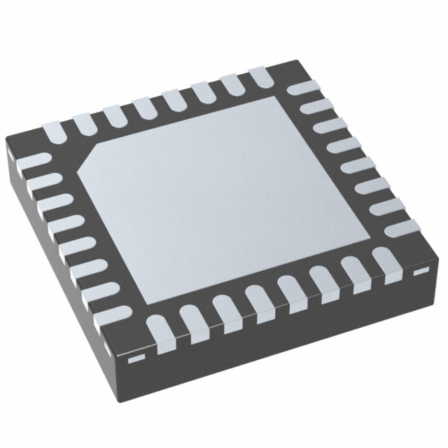


 工商网监
湘ICP备2023018690号
工商网监
湘ICP备2023018690号

