CDCVF857
www.ti.com
SCAS047F – MARCH 2003 – REVISED MAY 2007
2.5-V PHASE-LOCKED-LOOP CLOCK DRIVER
FEATURES
•
•
•
•
•
•
•
•
•
•
•
•
•
•
DESCRIPTION
Spread-Spectrum Clock Compatible
Operating Frequency: 60 MHz to 220 MHz
Low Jitter (Cycle-Cycle): ±35 ps
Low Static Phase Offset: ±50 ps
Low Jitter (Period): ±30 ps
1-to-10 Differential Clock Distribution (SSTL2)
Best in Class for VOX = VDD/2 ±0.1 V
Operates From Dual 2.6-V or 2.5-V Supplies
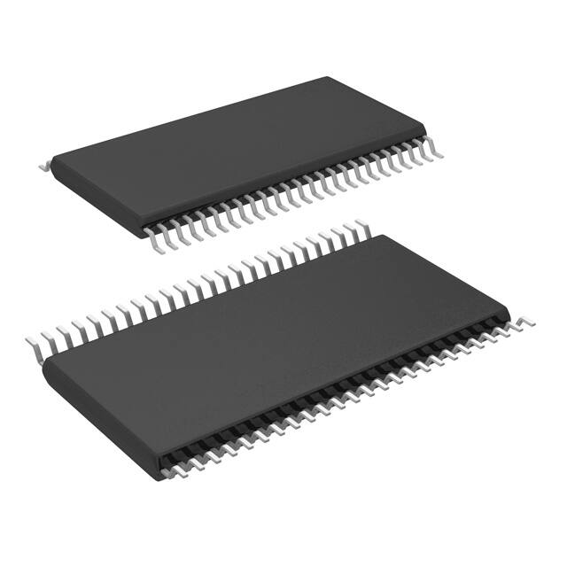
Available in a 40-Pin MLF Package, 48-Pin
TSSOP Package, 56-Ball MicroStar Junior™
BGA Package
Consumes < 100-µA Quiescent Current
External Feedback Pins (FBIN, FBIN) Are Used
to Synchronize the Outputs to the Input
Clocks
Meets/Exceeds JEDEC Standard (JESD82-1)
For DDRI-200/266/333 Specification
Meets/Exceeds Proposed DDRI-400
Specification (JESD82-1A)
Enters Low-Power Mode When No CLK Input
Signal Is Applied or PWRDWN Is Low
The CDCVF857 is a high-performance, low-skew,
low-jitter, zero-delay buffer that distributes a
differential clock input pair (CLK, CLK) to 10
differential pairs of clock outputs (Y[0:9], Y[0:9]) and
one differential pair of feedback clock outputs
(FBOUT, FBOUT). The clock outputs are controlled
by the clock inputs (CLK, CLK), the feedback clocks
(FBIN, FBIN), and the analog power input (AVDD).
When PWRDWN is high, the outputs switch in phase
and frequency with CLK. When PWRDWN is low, all
outputs are disabled to a high-impedance state
(3-state) and the PLL is shut down (low-power
mode). The device also enters this low-power mode
when the input frequency falls below a suggested
detection frequency that is below 20 MHz (typical 10
MHz). An input frequency detection circuit detects
the low frequency condition and, after applying a
>20-MHz input signal, this detection circuit turns the
PLL on and enables the outputs.
When AVDD is strapped low, the PLL is turned off
and bypassed for test purposes. The CDCVF857 is
also able to track spread spectrum clocking for
reduced EMI.
Because the CDCVF857 is based on PLL circuitry, it
requires a stabilization time to achieve phase-lock of
the PLL. This stabilization time is required following
power up. The CDCVF857 is characterized for both
commercial and industrial temperature ranges.
APPLICATIONS
•
•
DDR Memory Modules (DDR400/333/266/200)
Zero-Delay Fan-Out Buffer
A
A
AVAILABLE OPTIONS
TA
TSSOP (DGG)
–40°C to 85°C
CDCVF857DGG
–40°C to 85°C
(1)
40-Pin MLF
56-Ball BGA (1)
CDCVF857RTB
CDCVF857GQL
CDCVF857RHA
CDCVF857ZQL
Maximum load recommended is 12 pf for 200 MHz. At 12-pf load, maximum TA allowed is 70°C.
Please be aware that an important notice concerning availability, standard warranty, and use in critical applications of Texas
Instruments semiconductor products and disclaimers thereto appears at the end of this data sheet.
MicroStar Junior is a trademark of Texas Instruments.
PRODUCTION DATA information is current as of publication date.
Products conform to specifications per the terms of the Texas
Instruments standard warranty. Production processing does not
necessarily include testing of all parameters.
Copyright © 2003–2007, Texas Instruments Incorporated
�CDCVF857
www.ti.com
SCAS047F – MARCH 2003 – REVISED MAY 2007
FUNCTION TABLE
(Select Functions)
INPUTS
OUTPUTS
AVDD
PWRDWN
CLK
CLK
Y[0:9]
Y[0:9]
FBOUT
FBOUT
GND
H
L
H
L
H
L
H
Bypassed/off
GND
H
H
L
H
L
H
L
Bypassed/off
X
L
L
H
Z
Z
Z
Z
Off
X
L
H
L
Z
Z
Z
Z
Off
2.5 V (nom)
H
L
H
L
H
L
H
On
2.5 V (nom)
H
H
L
H
L
H
L
On
2.5 V (nom)
X
VDDQ
±50 mA
IO
Continuous output current
VO = 0 to VDDQ
IDDC
Continuous current to GND or VDDQ
Tstg
Storage temperature range
(1)
(2)
(3)
0.5 V to 3.6 V
–0.5 V to VDDQ + 0.5 V
–0.5 V to VDDQ + 0.5 V
±50 mA
±100 mA
–65°C to 150°C
Stresses beyond those listed under "absolute maximum ratings" may cause permanent damage to the device. These are stress ratings
only, and functional operation of the device at these or any other conditions beyond those indicated under "recommended operating
conditions" is not implied. Exposure to absolute-maximum-rated conditions for extended periods may affect device reliability.
The input and output negative voltage ratings may be exceeded if the input and output clamp current ratings are observed.
This value is limited to 3.6 V maximum.
THERMAL CHARACTERISTICS
RθJA for TSSOP (DGG) Package (1)
(1)
(2)
RθJA for MLF (RHA/RTB) Package
RθJA for BGA (GQL/ZQL) Package (2)
Airflow
Low K
High K
Airflow
With 4 Thermal Vias
Airflow
High K
0 ft/min
89.1°C/W
70°C/W
0 ft/min
44.7°C/W
0 ft/min
132.2°C/W
150 ft/min
78.5°C/W
65.3°C/W
150 ft/min
150 ft/min
126.4°C/W
The package thermal impedance is calculated in accordance with JESD 51.
Connecting the NC-balls (C3, C4, D3, D4, G3, G4, H3, H4) to a ground plane improves the θJA to 114.8°C/W (0 airflow).
Submit Documentation Feedback
5
�CDCVF857
www.ti.com
SCAS047F – MARCH 2003 – REVISED MAY 2007
RECOMMENDED OPERATING CONDITIONS
MIN
VDDQ
Supply voltage
PC1600 – PC3200
AVDD
VIL
Low-level input voltage
VIH
High-level input voltage
DC input signal voltage
NOM
MAX
2.3
2.7
VDDQ – 0.12
2.7
CLK, CLK, FBIN, FBIN
VDDQ/2 – 0.18
PWRDWN
–0.3
CLK, CLK, FBIN, FBIN
VDDQ/2 + 0.18
PWRDWN
(1)
(2)
0.7
1.7
VDDQ + 0.3
–0.3
VDDQ + 0.3
DC
CLK, FBIN
0.36
VDDQ + 0.6
AC
CLK, FBIN
0.7
VDDQ + 0.6
VDDQ/2 – 0.2
VDDQ/2 + 0.2
UNIT
V
V
V
V
VID
Differential input signal voltage
VIX
Input differential pair cross voltage
IOH
High-level output current
–12
IOL
Low-level output current
12
mA
SR
Input slew rate
1
4
V/ns
TA
Operating free-air temperature
–40
85
°C
(1)
(2)
(3)
(4)
(3) (4)
V
V
mA
The unused inputs must be held high or low to prevent them from floating.
The dc input signal voltage specifies the allowable dc execution of the differential input.
The differential input signal voltage specifies the differential voltage |VTR – VCP| required for switching, where VTR is the true input
level and VCP is the complementary input level.
The differential cross-point voltage tracks variations of VCC and is the voltage at which the differential signals must cross.
ELECTRICAL CHARACTERISTICS
over recommended operating free-air temperature range (unless otherwise noted)
PARAMETER
VIK
TEST CONDITIONS
Input voltage, all inputs
VDDQ = min to max, IOH = –1 mA
High-level output voltage
VOL
Low-level output voltage
VOD
Output voltage swing
VOX
Output differential
cross-voltage (3)
II
Input current
IOZ
High-impedance-state output
VDDQ = 2.7 V, VO = VDDQ or GND
current
IDDPD
Power-down current on VDDQ CLK and CLK = 0 MHz; PWRDWN =
+ AVDD
Low; Σ of IDD and AIDD
AIDD
Supply current on AVDD
CI
Input capacitance
VDDQ = 2.3 V, IOH = –12 mA
(3)
6
MAX
UNIT
–1.2
V
V
1.7
VDDQ = min to max, IOL = 1 mA
0.1
VDDQ = 2.3 V, IOL = 12 mA
0.6
Differential outputs are terminated with
120 Ω, CL = 14 pF (see Figure 3)
1.1
VDDQ/2 – 0.1
VDDQ/2
VDDQ = 2.7 V, VI = 0 V to 2.7 V
20
V
VDDQ/2 + 0.1
V
±10
µA
±10
µA
100
µA
6
8
fO = 200 MHz
8
10
2.5
3.5
fO = 170 MHz
120
140
fO = 200 MHz
125
150
Differential outputs
fO = 170 MHz
terminated with 120 Ω, CL
fO = 200 MHz
= 0 pF
220
270
230
280
Differential outputs
fO = 170 MHz
terminated with 120 Ω, CL
fO = 200 MHz
= 14 pF
280
330
300
350
VDDQ = 2.5 V, VI = VDDQ or GND
2
V
VDDQ – 0.4
fO = 170 MHz
Without load
(1)
(2)
(1)
VDDQ – 0.1
(2)
Dynamic current on VDDQ
TYP
VDDQ = 2.3 V, II = –18 mA
VOH
IDD
MIN
mA
pF
mA
All typical values are at nominal VDDQ.
The differential output signal voltage specifies the differential voltage |VTR – VCP|, where VTR is the true output level and VCP is the
complementary output level.
The differential cross-point voltage tracks variations of VDDQ and is the voltage at which the differential signals must cross.
Submit Documentation Feedback
�CDCVF857
www.ti.com
SCAS047F – MARCH 2003 – REVISED MAY 2007
ELECTRICAL CHARACTERISTICS (continued)
over recommended operating free-air temperature range (unless otherwise noted)
PARAMETER
TEST CONDITIONS
MIN
TYP
(1)
MAX
UNIT
∆C
Part-to-part input
capacitance variation
VDDQ = 2.5 V, VI = VDDQ or GND
1
pF
CI(∆)
Input capacitance difference
between CLK and CLK,
FBIN, and FBIN
VDDQ = 2.5 V, VI = VDDQ or GND
0.25
pF
TIMING REQUIREMENTS
over recommended ranges of supply voltage and operating free-air temperature
PARAMETER
fCLK
MIN
MAX
Operating clock frequency
60
220
Application clock frequency
90
220
40%
60%
Input clock duty cycle
Stabilization time (PLL mode)
(1)
Stabilization time (bypass mode)
(1)
(2)
(2)
UNIT
MHz
10
µs
30
ns
The time required for the integrated PLL circuit to obtain phase lock of its feedback signal to its reference signal. For phase lock to be
obtained, a fixed-frequency, fixed-phase reference signal must be present at CLK and VDD must be applied. Until phase lock is obtained,
the specifications for propagation delay, skew, and jitter parameters given in the switching characteristics table are not applicable. This
parameter does not apply for input modulation under SSC application.
A recovery time is required when the device goes from power-down mode into bypass mode (AVDD at GND).
SWITCHING CHARACTERISTICS
over operating free-air temperature range (unless otherwise noted)
PARAMETER
TEST CONDITIONS
MIN
TYP
(1)
Low-to-high level propagation delay time
Test mode/CLK to any output
3.5
tPHL (1)
High-to-low level propagation delay time
Test mode/CLK to any output
3.5
tPLH
ns
–65
65
133/167/200 MHz (PC2100/2700/3200)
–30
30
100 MHz (PC1600)
–50
50
133/167/200 MHz (PC2100/2700/3200)
–35
35
–100
100
–75
75
Jitter (period), see Figure 7
tjit(cc) (2)
Jitter (cycle-to-cycle), see Figure 4
tjit(hper) (2)
Half-period jitter, see Figure 8
tslr(o)
Output clock slew rate, see Figure 9
Load: 120 Ω, 14 pF
t(φ)
Static phase offset, see Figure 5
100/133/167/200 MHz
tsk(o)
Output skew, see Figure 6
Load: 120 Ω, 14 pF; 100/133/167/200 MHz
100 MHz (PC1600)
133/167/200 MHz (PC2100/2700/3200)
UNIT
ns
100 MHz (PC1600)
tjit(per) (2)
(1)
(2)
MAX
ps
ps
ps
1
2
V/ns
–50
50
ps
40
ps
Refers to the transition of the noninverting output.
This parameter is assured by design but cannot be 100% production tested.
Submit Documentation Feedback
7
�CDCVF857
www.ti.com
SCAS047F – MARCH 2003 – REVISED MAY 2007
PARAMETER MEASUREMENT INFORMATION
VDD
VYx
R = 60 W
R = 60 W
VDD/2
VYx
CDCVF857
GND
S0229-01
Figure 1. IBIS Model Output Load
VDD/2
C = 14 pF
R = 10 W
Z = 60 W
–VDD/2
Scope
Z = 50 W
R = 50 W
V(TT)
Z = 60 W
R = 10 W
Z = 50 W
C = 14 pF
CDCVF857
–VDD/2
R = 50 W
V(TT)
–VDD/2
V(TT) = GND
S0230-01
Figure 2. Output Load Test Circuit
8
Submit Documentation Feedback
�CDCVF857
www.ti.com
SCAS047F – MARCH 2003 – REVISED MAY 2007
PARAMETER MEASUREMENT INFORMATION (continued)
VDD
C = 14 pF
Probe
GND
Z = 60 W
C = 1 pF
R = 120 W
R = 1 MW
V(TT)
Z = 60 W
C = 1 pF
C = 14 pF
CDCVF857
R = 1 MW
V(TT)
GND
GND
V(TT) = GND
S0231-01
Figure 3. Output Load Test Circuit for Crossing Point
Yx, FBOUT
Yx, FBOUT
tc(n)
tc(n +1)
tjit(cc) = tc(n) – tc(n+1)
T0174-01
Figure 4. Cycle-to-Cycle Jitter
CLK
CLK
FBIN
FBIN
t(f)n
t(f)n+1
t(f) =
S
n=N
t(f)n
1
N
(N > 1000 Samples)
T0175-01
Figure 5. Phase Offset
Submit Documentation Feedback
9
�CDCVF857
www.ti.com
SCAS047F – MARCH 2003 – REVISED MAY 2007
PARAMETER MEASUREMENT INFORMATION (continued)
Yx
Yx
Yx, FBOUT
Yx, FBOUT
tsk(o)
T0176-01
Figure 6. Output Skew
Yx, FBOUT
Yx, FBOUT
tc(n)
Yx, FBOUT
Yx, FBOUT
1
f0
1
f0
tjit(per) = tc(n) –
f0 = Average Input Frequency Measured at CLK/CLK
T0177-01
Figure 7. Period Jitter
Yx, FBOUT
Yx, FBOUT
t(hper_n)
t(hper_n+1)
1
f0
n = Any Half Cycle
tjit(hper) = t(hper_n) –
1
2´f0
f0 = Average Input Frequency Measured at CLK/CLK
T0178-01
Figure 8. Half-Period Jitter
10
Submit Documentation Feedback
�CDCVF857
www.ti.com
SCAS047F – MARCH 2003 – REVISED MAY 2007
PARAMETER MEASUREMENT INFORMATION (continued)
VOH, VIH
80%
Clock Inputs
and Outputs
80%
20%
20%
VOL, VIL
tr
tslr(I/O) =
tf
V80% – V20%
tslf(I/O) =
tr
V80% – V20%
tf
T0179-01
Figure 9. Input and Output Slew Rates
(2)
Card
Via
Bead
0603
AVDD
VDDQ
4.7 mF
1206
0.1 mF
0603
GND
Card
Via
(1)
2200 pF
0603
PLL
AGND
S0232-01
(1)
Place the 2200-pF capacitor close to the PLL.
(2)
Recommended bead: Fair-Rite P/N 2506036017Y0 or equilvalent (0.8 Ω dc maximum, 600 Ω at 100 MHz).
NOTE: Use a wide trace for the PLL analog power and ground. Connect PLL and capacitors to AGND trace and connect
trace to one GND via (farthest from the PLL).
Figure 10. Recommended AVDD Filtering
Submit Documentation Feedback
11
�PACKAGE OPTION ADDENDUM
www.ti.com
19-Oct-2022
PACKAGING INFORMATION
Orderable Device
Status
(1)
Package Type Package Pins Package
Drawing
Qty
Eco Plan
(2)
Lead finish/
Ball material
MSL Peak Temp
Op Temp (°C)
Device Marking
(3)
Samples
(4/5)
(6)
CDCVF857DGG
ACTIVE
TSSOP
DGG
48
40
RoHS & Green
NIPDAU
Level-2-260C-1 YEAR
-40 to 85
CDCVF857
Samples
CDCVF857DGGR
ACTIVE
TSSOP
DGG
48
2000
RoHS & Green
NIPDAU
Level-2-260C-1 YEAR
-40 to 85
CDCVF857
Samples
CDCVF857DGGRG4
ACTIVE
TSSOP
DGG
48
2000
RoHS & Green
NIPDAU
Level-2-260C-1 YEAR
-40 to 85
CDCVF857
Samples
CDCVF857RHAT
ACTIVE
VQFN
RHA
40
250
RoHS & Green
NIPDAU
Level-3-260C-168 HR
-40 to 85
CKVF857
Samples
(1)
The marketing status values are defined as follows:
ACTIVE: Product device recommended for new designs.
LIFEBUY: TI has announced that the device will be discontinued, and a lifetime-buy period is in effect.
NRND: Not recommended for new designs. Device is in production to support existing customers, but TI does not recommend using this part in a new design.
PREVIEW: Device has been announced but is not in production. Samples may or may not be available.
OBSOLETE: TI has discontinued the production of the device.
(2)
RoHS: TI defines "RoHS" to mean semiconductor products that are compliant with the current EU RoHS requirements for all 10 RoHS substances, including the requirement that RoHS substance
do not exceed 0.1% by weight in homogeneous materials. Where designed to be soldered at high temperatures, "RoHS" products are suitable for use in specified lead-free processes. TI may
reference these types of products as "Pb-Free".
RoHS Exempt: TI defines "RoHS Exempt" to mean products that contain lead but are compliant with EU RoHS pursuant to a specific EU RoHS exemption.
Green: TI defines "Green" to mean the content of Chlorine (Cl) and Bromine (Br) based flame retardants meet JS709B low halogen requirements of


 工商网监
湘ICP备2023018690号
工商网监
湘ICP备2023018690号
