Order
Now
Product
Folder
Support &
Community
Tools &
Software
Technical
Documents
CSD87501L
SLPS523B – FEBRUARY 2015 – REVISED MAY 2019
CSD87501L 30-V Dual Common Drain N-Channel NexFET™ Power MOSFET
1 Features
•
•
•
•
•
•
•
1
Product Summary
Low on-resistance
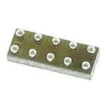
Small footprint of 3.37 mm × 1.47 mm
Ultra-low profile – 0.2-mm high
Lead free
RoHS compliant
Halogen free
Gate ESD protection
TA = 25°C
TYPICAL VALUE
UNIT
30
V
Gate Charge Total (4.5 V)
15
nC
Gate Charge Gate-to-Drain
6.0
VS1S2
Source-to-Source Voltage
Qg
Qgd
RS1S2(on)
Source-to-Source OnResistance
VGS(th)
Threshold Voltage
2 Applications
•
•
•
This 30-V, 6.6-mΩ, 3.37-mm × 1.47-mm LGA Dual
NexFET™ power MOSFET is designed to minimize
resistance and gate charge in a small footprint. Its
small size and common drain configuration make the
device ideal for multi-cell battery pack applications
and small handheld devices.
Top View
S1
S2
G1
G2
S1
S1
S2
S2
6.6
1.8
mΩ
V
DEVICE
MEDIA
QTY
PACKAGE
SHIP
CSD87501L
7-Inch Reel
3000
CSD87501LT
7-Inch Reel
250
3.37 mm × 1.47 mm
Land Grid Array
Package
Tape
and
Reel
Source 1
Absolute Maximum Ratings
TA = 25°C
VALUE
UNIT
VS1S2
Source-to-Source Voltage
30
V
VGS
Gate-to-Source Voltage
±20
V
IS
Continuous Source Current(1)
14
A
ISM
Pulsed Source Current(2)
72
A
PD
Power Dissipation
2.5
W
V(ESD)
Human-Body Model (HBM)
2
kV
TJ,
Tstg
Operating Junction,
Storage Temperature
–55 to 150
°C
(1) Typical RθJA = 50°C/W on a 1-in2, 2-oz Cu pad on a 0.06-in
thick FR4 PCB.
(2) Typical min Cu RθJA = 135°C/W, pulse duration ≤ 100 μs, duty
cycle ≤ 1%.
Configuration
Source 2
Gate 1
Gate 2
RS1S2(on) vs VGS
Gate Charge
10
24
TC = 25°C, I S = 7 A
TC = 125°C, I S = 7 A
21
VGS - Gate-to-Source Voltage (V)
RS1S2(on) - On-State Resistance (m:)
VGS = 10 V
(1) For all available packages, see the orderable addendum at
the end of the data sheet.
3 Description
S2
9.3
Device Information(1)
Battery management
Battery protection
USB Type-C / PD
S1
nC
VGS = 4.5 V
18
15
12
9
6
3
0
IS = 7 A, VS1S2 = 15 V
9
8
7
6
5
4
3
2
1
0
0
2
4
6
8
10
12
14
16
VGS - Gate-to-Source Voltage (V)
18
20
D007
0
4
8
12
16
20
Qg - Gate Charge (nC)
24
28
32
D004
1
An IMPORTANT NOTICE at the end of this data sheet addresses availability, warranty, changes, use in safety-critical applications,
intellectual property matters and other important disclaimers. PRODUCTION DATA.
�CSD87501L
SLPS523B – FEBRUARY 2015 – REVISED MAY 2019
www.ti.com
Table of Contents
1
2
3
4
5
Features ..................................................................
Applications ...........................................................
Description .............................................................
Revision History.....................................................
Specifications.........................................................
1
1
1
2
3
5.1 Electrical Characteristics........................................... 3
5.2 Thermal Information .................................................. 3
5.3 Typical MOSFET Characteristics.............................. 4
6
Device and Documentation Support.................... 7
6.1
6.2
6.3
6.4
6.5
7
Receiving Notification of Documentation Updates....
Community Resources..............................................
Trademarks ...............................................................
Electrostatic Discharge Caution ................................
Glossary ....................................................................
7
7
7
7
7
Mechanical, Packaging, and Orderable
Information ............................................................. 8
7.1 Package Dimensions ................................................ 8
7.2 Recommended PCB Pattern..................................... 9
7.3 Recommended Stencil Pattern ................................. 9
4 Revision History
Changes from Revision A (April 2015) to Revision B
Page
•
Added Receiving Notification of Documentation Updates section and Community Resources section ................................ 7
•
Added Pin Configuration table in the Mechanical, Packaging, and Orderable Information section ....................................... 8
Changes from Original (February 2015) to Revision A
•
2
Page
Extended Y axis in Figure 9 down to 0.01 A .......................................................................................................................... 4
Submit Documentation Feedback
Copyright © 2015–2019, Texas Instruments Incorporated
Product Folder Links: CSD87501L
�CSD87501L
www.ti.com
SLPS523B – FEBRUARY 2015 – REVISED MAY 2019
5 Specifications
5.1 Electrical Characteristics
TA = 25°C unless otherwise stated
PARAMETER
TEST CONDITIONS
MIN
TYP
MAX
UNIT
STATIC CHARACTERISTICS
BVS1S2
Source-to-source voltage
VGS = 0 V, IS = 250 μA
IS1S2
Source-to-source leakage current
VGS = 0 V, VS1S2 = 24 V
1
μA
IGSS
Gate-to-source leakage current
VS1S2 = 0 V, VGS = 20 V
10
µA
VGS(th)
Gate-to-source threshold voltage
VS1S2 = VGS, IS = 250 μA
V
RS1S2(on)
Source-to-source on-resistance
gfs
Transconductance
30
1.3
V
1.8
2.3
VGS = 4.5 V, IS = 7 A
9.3
11.0
VGS = 10 V, IS = 7 A
6.6
7.8
VS1S2 = 3 V, IS = 7 A
48
mΩ
S
DYNAMIC CHARACTERISTICS (1)
Ciss
Input capacitance
Coss
Output capacitance
1620
2110
pF
189
246
pF
Crss
RG
Reverse transfer capacitance
152
198
pF
Series gate resistance
300
450
Qg
Gate charge total (4.5 V)
Ω
15
20
nC
Qg
Gate charge total (10 V)
Qgd
Gate charge gate-to-drain
31
40
nC
Qgs
Gate charge gate-to-source
Qg(th)
Gate charge at Vth
Qoss
Output charge
td(on)
VGS = 0 V, VS1S2 = 15 V, ƒ = 1 MHz
6.0
nC
5.0
nC
2.5
nC
7.6
nC
Turn on delay time
164
ns
tr
Rise time
260
ns
td(off)
Turn off delay time
709
ns
tf
Fall time
712
ns
(1)
VS1S2 = 15 V, IS = 7 A
VS1S2 = 15 V, VGS = 0 V
VS1S2 = 15 V, VGS = 10 V,
IS1S2 = 7 A, RG = 0 Ω
Dynamic characteristics values specified are per single FET.
5.2 Thermal Information
TA = 25°C unless otherwise stated
THERMAL METRIC
RθJA
(1)
(2)
MIN
TYP
Junction-to-ambient thermal resistance (1)
135
Junction-to-ambient thermal resistance (2)
50
MAX
UNIT
°C/W
Device mounted on FR4 material with minimum Cu mounting area.
Device mounted on FR4 material with 1-in2 (6.45-cm2), 2-oz (0.071-mm thick) Cu.
Submit Documentation Feedback
Copyright © 2015–2019, Texas Instruments Incorporated
Product Folder Links: CSD87501L
3
�CSD87501L
SLPS523B – FEBRUARY 2015 – REVISED MAY 2019
www.ti.com
5.3 Typical MOSFET Characteristics
TA = 25°C unless otherwise stated
Figure 1. Transient Thermal Impedance
50
IS1S2 - Source-to-Source Current (A)
IS1S2 - Source-to-Source Current (A)
50
40
30
20
10
VGS = 4.5 V
VGS = 6 V
VGS = 10 V
0
45
40
35
30
25
20
15
10
TC = 125°C
TC = 25°C
TC = -55°C
5
0
0
0.1
0.2
0.3
0.4
0.5
VS1S2 - Source-to-Source Voltage (V)
0.6
0
D002
0.5
1
1.5
2
2.5
VS1S2 - Source-to-Source Voltage (V)
3
3.5
D003
VS1S2 = 15 V
Figure 2. Saturation Characteristics
4
Submit Documentation Feedback
Figure 3. Transfer Characteristics
Copyright © 2015–2019, Texas Instruments Incorporated
Product Folder Links: CSD87501L
�CSD87501L
www.ti.com
SLPS523B – FEBRUARY 2015 – REVISED MAY 2019
Typical MOSFET Characteristics (continued)
TA = 25°C unless otherwise stated
10000
9
8
C - Capacitance (pF)
VGS - Gate-to-Source Voltage (V)
10
7
6
5
4
3
1000
100
2
Ciss = Cgd + Cgs
Coss = Cds + Cgd
Crss = Cgd
1
0
10
0
4
8
12
16
20
Qg - Gate Charge (nC)
IS = 7 A
24
28
32
0
3
6
9
12
15
18
21
24
VS1S2 - Source-to-Source Voltage (V)
D004
D005
Figure 5. Capacitance
2.4
24
RS1S2(on) - On-State Resistance (m:)
VGS(th) - Threshold Voltage (V)
30
VS1S2 = 15 V
Figure 4. Gate Charge
2.2
2
1.8
1.6
1.4
1.2
1
-75
27
TC = 25°C, I S = 7 A
TC = 125°C, I S = 7 A
21
18
15
12
9
6
3
0
-50
-25
0
25
50
75 100
TC - Case Temperature (°C)
125
150
175
0
2
4
D006
6
8
10
12
14
16
VGS - Gate-to-Source Voltage (V)
18
20
D007
IS = 250 µA
Figure 6. Threshold Voltage vs Temperature
Figure 7. On-State Source-to-Source Resistance vs
Gate-to-Source Voltage
1.6
100
VGS = 4.5 V
VGS = 10 V
IS1S2 - Source-to-Source Current (A)
Normalized On-State Resistance
1.8
1.4
1.2
1
0.8
0.6
-75
-50
-25
0
25
50
75 100
TC - Case Temperature (°C)
125
150
175
10
1
0.1
100 ms
10 ms
1 ms
0.01
0.1
100 µs
10 µs
1
10
VS1S2 - Source-to-Source Voltage (V)
D008
IS = 7 A
100
D009
Single pulse, max RθJA = 135°C/W
Figure 8. Normalized On-State Resistance vs Temperature
Figure 9. Maximum Safe Operating Area
Submit Documentation Feedback
Copyright © 2015–2019, Texas Instruments Incorporated
Product Folder Links: CSD87501L
5
�CSD87501L
SLPS523B – FEBRUARY 2015 – REVISED MAY 2019
www.ti.com
Typical MOSFET Characteristics (continued)
TA = 25°C unless otherwise stated
IS1S2 - Source-to-Source Current (A)
14
12
10
8
6
4
2
0
-50
-25
0
25
50
75
100 125
TC - Case Temperature (°C)
150
175
D010
Figure 10. Maximum Source Current vs Temperature
6
Submit Documentation Feedback
Copyright © 2015–2019, Texas Instruments Incorporated
Product Folder Links: CSD87501L
�CSD87501L
www.ti.com
SLPS523B – FEBRUARY 2015 – REVISED MAY 2019
6 Device and Documentation Support
6.1 Receiving Notification of Documentation Updates
To receive notification of documentation updates, navigate to the device product folder on ti.com. In the upper
right corner, click on Alert me to register and receive a weekly digest of any product information that has
changed. For change details, review the revision history included in any revised document.
6.2 Community Resources
The following links connect to TI community resources. Linked contents are provided "AS IS" by the respective
contributors. They do not constitute TI specifications and do not necessarily reflect TI's views; see TI's Terms of
Use.
TI E2E™ Online Community TI's Engineer-to-Engineer (E2E) Community. Created to foster collaboration
among engineers. At e2e.ti.com, you can ask questions, share knowledge, explore ideas and help
solve problems with fellow engineers.
Design Support TI's Design Support Quickly find helpful E2E forums along with design support tools and
contact information for technical support.
6.3 Trademarks
NexFET, E2E are trademarks of Texas Instruments.
All other trademarks are the property of their respective owners.
6.4 Electrostatic Discharge Caution
These devices have limited built-in ESD protection. The leads should be shorted together or the device placed in conductive foam
during storage or handling to prevent electrostatic damage to the MOS gates.
6.5 Glossary
SLYZ022 — TI Glossary.
This glossary lists and explains terms, acronyms, and definitions.
Submit Documentation Feedback
Copyright © 2015–2019, Texas Instruments Incorporated
Product Folder Links: CSD87501L
7
�CSD87501L
SLPS523B – FEBRUARY 2015 – REVISED MAY 2019
www.ti.com
7 Mechanical, Packaging, and Orderable Information
The following pages include mechanical, packaging, and orderable information. This information is the most
current data available for the designated devices. This data is subject to change without notice and revision of
this document. For browser-based versions of this data sheet, refer to the left-hand navigation.
7.1 Package Dimensions
0.65 TYP
B
1.52
1.42
0.325 TYP
A
2
1
0.65 TYP
A
PIN A1
CORNER
B
SYMM
3.42
3.32
2X
C
2.6
D
E
0.33
0.27
C A
B
10X
0.015
SYMM
0.200±0.02
C
SEATING PLANE
All dimensions in millimeters.
Table 1. Pin Configuration
8
Position
Designation
A1, B1, D1, E1
Source 1
C1
Gate 1
A2, B2, D2, E2
Source 2
C2
Gate 2
Submit Documentation Feedback
Copyright © 2015–2019, Texas Instruments Incorporated
Product Folder Links: CSD87501L
�CSD87501L
www.ti.com
SLPS523B – FEBRUARY 2015 – REVISED MAY 2019
7.2 Recommended PCB Pattern
(0.65) TYP
10X ( 0.3)
2
1
A
(0.65) TYP
B
SYMM
C
D
E
SYMM
LAND PATTERN EXAMPLE
7.3 Recommended Stencil Pattern
(0.65) TYP
10X ( 0.3)
1
2
A
(0.65)
TYP
(R0.05) TYP
B
SYMM
C
METAL
TYP
D
E
SYMM
All dimensions are in millimeters unless otherwise
SOLDER noted.
PASTE EXAMPLE
www.ti.com
Submit Documentation Feedback
Copyright © 2015–2019, Texas Instruments Incorporated
Product Folder Links: CSD87501L
9
�PACKAGE OPTION ADDENDUM
www.ti.com
11-Jan-2022
PACKAGING INFORMATION
Orderable Device
Status
(1)
Package Type Package Pins Package
Drawing
Qty
Eco Plan
(2)
Lead finish/
Ball material
MSL Peak Temp
Op Temp (°C)
Device Marking
(3)
(4/5)
(6)
CSD87501L
ACTIVE
PICOSTAR
YJG
10
3000
RoHS & Green
NIAU
Level-1-260C-UNLIM
CSD87501LT
ACTIVE
PICOSTAR
YJG
10
250
RoHS & Green
NIAU
Level-1-260C-UNLIM
CSD87501
-55 to 150
CSD87501
(1)
The marketing status values are defined as follows:
ACTIVE: Product device recommended for new designs.
LIFEBUY: TI has announced that the device will be discontinued, and a lifetime-buy period is in effect.
NRND: Not recommended for new designs. Device is in production to support existing customers, but TI does not recommend using this part in a new design.
PREVIEW: Device has been announced but is not in production. Samples may or may not be available.
OBSOLETE: TI has discontinued the production of the device.
(2)
RoHS: TI defines "RoHS" to mean semiconductor products that are compliant with the current EU RoHS requirements for all 10 RoHS substances, including the requirement that RoHS substance
do not exceed 0.1% by weight in homogeneous materials. Where designed to be soldered at high temperatures, "RoHS" products are suitable for use in specified lead-free processes. TI may
reference these types of products as "Pb-Free".
RoHS Exempt: TI defines "RoHS Exempt" to mean products that contain lead but are compliant with EU RoHS pursuant to a specific EU RoHS exemption.
Green: TI defines "Green" to mean the content of Chlorine (Cl) and Bromine (Br) based flame retardants meet JS709B low halogen requirements of