DAC2900
DAC
290
0
www.ti.com
SBAS166C – JUNE 2001 – REVISED SEPTEMBER 2008
Dual, 10-Bit, 125MSPS
DIGITAL-TO-ANALOG CONVERTER
FEATURES
APPLICATIONS
●
●
●
●
●
●
●
● COMMUNICATIONS:
Base Stations, WLL, WLAN
Baseband I/Q Modulation
125MSPS UPDATE RATE
SINGLE SUPPLY: +3.3V or +5V
HIGH SFDR: 68dB at fOUT = 20MHz
LOW GLITCH: 2pV-s
LOW POWER: 310mW at +5V
INTERNAL REFERENCE
POWER-DOWN MODE: 23mW
● MEDICAL/TEST INSTRUMENTATION
● ARBITRARY WAVEFORM GENERATORS (ARB)
● DIRECT DIGITAL SYNTHESIS (DDS)
DESCRIPTION
The DAC2900 is a monolithic, 10-bit, dual-channel,
high-speed Digital-to-Analog Converter (DAC), and is
optimized to provide high dynamic performance while
dissipating only 310mW on a +5V single supply.
The DAC2900 combines high dynamic performance with
a high throughput rate to create a cost-effective solution
for a wide variety of waveform-synthesis applications:
• Pin compatibility between family members provides
10-bit (DAC2900), 12-bit (DAC2902), and 14-bit
(DAC2904) resolution.
Operating with high update rates of up to 125MSPS, the
DAC2900 offers exceptional dynamic performance, and
enables the generation of very high output frequencies
suitable for Direct IF applications. The DAC2900 has
been optimized for communications applications in which
separate I and Q data are processed while maintaining
tight gain and offset matching.
• Pin compatible to the AD9763 dual DAC.
Each DAC has a high-impedance differential-current
output, suitable for single-ended or differential analog
output configurations.
• All digital inputs are +3.3V and +5V logic compatible.
The DAC2900 has an internal reference circuit, and
allows use of an external reference.
• Gain matching is typically 0.5% of full-scale, and offset
matching is specified at 0.02% max.
• The DAC2900 utilizes an advanced CMOS process; the
segmented architecture minimizes output glitch energy,
and maximizes dynamic performance.
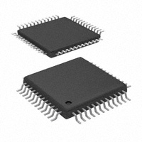
• The DAC2900 is available in a TQFP-48 package, and
is specified over the extended industrial temperature
range of –40°C to +85°C.
Please be aware that an important notice concerning availability, standard warranty, and use in critical applications of
Texas Instruments semiconductor products and disclaimers thereto appears at the end of this data sheet.
All trademarks are the property of their respective owners.
Copyright © 2001-2008, Texas Instruments Incorporated
PRODUCTION DATA information is current as of publication date.
Products conform to specifications per the terms of Texas Instruments
standard warranty. Production processing does not necessarily include
testing of all parameters.
www.ti.com
�ABSOLUTE MAXIMUM RATINGS
ELECTROSTATIC
DISCHARGE SENSITIVITY
+VA to AGND ........................................................................ –0.3V to +6V
+VD to DGND ........................................................................ –0.3V to +6V
AGND to DGND ................................................................. –0.3V to +0.3V
+VA to +VD ............................................................................... –6V to +6V
CLK, PD to DGND ..................................................... –0.3V to VD + 0.3V
D0-D9 to DGND ......................................................... –0.3V to VD + 0.3V
IOUT, IOUT to AGND ........................................................ –1V to VA + 0.3V
BW, BYP to AGND ..................................................... –0.3V to VA + 0.3V
REFIN, FSA to AGND ................................................. –0.3V to VA + 0.3V
INT/EXT to AGND ...................................................... –0.3V to VA + 0.3V
Junction Temperature .................................................................... +150°C
Case Temperature ......................................................................... +100°C
Storage Temperature .................................................................... +125°C
This integrated circuit can be damaged by ESD. Texas Instruments
recommends that all integrated circuits be handled with appropriate
precautions. Failure to observe proper handling and installation procedures can cause damage.
ESD damage can range from subtle performance degradation to
complete device failure. Precision integrated circuits may be more
susceptible to damage because very small parametric changes could
cause the device not to meet its published specifications.
PACKAGE/ORDERING INFORMATION(1)
SPECIFIED
TEMPERATURE
RANGE
PACKAGE
MARKING
ORDERING
NUMBER
TRANSPORT
MEDIA, QUANTITY
DAC2900Y/250
DAC2900Y/1K
Tape and Reel, 250
Tape and Reel, 1000
PRODUCT
PACKAGE
PACKAGE
DESIGNATOR
DAC2900Y
TQFP-48
PFB
–40°C to +85°C
DAC2900Y
"
"
"
"
"
NOTE: (1) For the most current package and ordering information, see the Package Option Addendum at the end of this document, or see the TI website at www.ti.com.
PRODUCT
DAC2900
EVM ORDERING NUMBER
DAC2900-EVM
COMMENT
Fully populated evaluation board. See user manual for details.
ELECTRICAL CHARACTERISTICS
At TMIN to TMAX, +VA = +5V, +VD = +3.3V, differential transformer coupled output, and 50Ω doubly-terminated, unless otherwise noted. Independent Gain mode.
DAC2900Y
PARAMETER
TEST CONDITIONS
MIN
RESOLUTION
Output Update Rate (fCLOCK)
STATIC ACCURACY(1)
Differential Nonlinearity (DNL)
Integral Nonlinearity (INL)
DYNAMIC PERFORMANCE
Spurious-Free Dynamic Range (SFDR)
fOUT = 1MHz, fCLOCK = 50MSPS
fOUT = 1MHz, fCLOCK = 26MSPS
fOUT = 2.18MHz, fCLOCK = 52MSPS
fOUT = 5.24MHz, fCLOCK = 52MSPS
fOUT = 10.4MHz, fCLOCK = 78MSPS
fOUT = 15.7MHz, fCLOCK = 78MSPS
fOUT = 5.04MHz, fCLOCK = 100MSPS
fOUT = 20.2MHz, fCLOCK = 100MSPS
fOUT = 20.1MHz, fCLOCK = 125MSPS
fOUT = 40.2MHz, fCLOCK = 125MSPS
Spurious-Free Dynamic Range within a Window
fOUT = 1.0MHz, fCLOCK = 50MSPS
fOUT = 5.02MHz, fCLOCK = 50MSPS
fOUT = 5.03MHz, fCLOCK = 78MSPS
fOUT = 5.04MHz, fCLOCK = 125MSPS
Total Harmonic Distortion (THD)
fOUT = 1MHz, fCLOCK = 50MSPS
fOUT = 5.02MHz, fCLOCK = 50MSPS
fOUT = 5.03MHz, fCLOCK = 78MSPS
fOUT = 5.04MHz, fCLOCK = 125MSPS
Multitone Power Ratio
fOUT = 2.0MHz to 2.99MHz, fCLOCK = 65MSPS
TYP
MAX
10
125
TA = +25°C
TMIN to TMAX
TA = +25°C
TMIN to TMAX
To Nyquist
0dBFS Output
–6dBFS Output
–12dBFS Output
2MHz Span
10MHz Span
10MHz Span
10MHz Span
+1.0
±0.25
–1.0
70
+1.0
LSB
LSB
LSB
LSB
80
75
70
80
80
80
75
71
80
68
61
56
dBc
dBc
dBc
dBc
dBc
dBc
dBc
dBc
dBc
dBc
dBc
dBc
86
80
80
80
dBc
dBc
dBc
dBc
–77
–74
–73
–70
8 Tone with 110kHz Spacing
0dBFS Output
Bits
MSPS
±0.25
–1.0
UNIT
80
–68
dBc
dBc
dBc
dBc
dBc
DAC2900
2
www.ti.com
SBAS166C
�ELECTRICAL CHARACTERISTICS (continued)
At TMIN to TMAX, +VA = +5V, +VD = +3.3V, differential transformer coupled output, and 50Ω doubly-terminated, unless otherwise noted. Independent Gain mode.
DAC2900Y
PARAMETER
DYNAMIC PERFORMANCE (Cont.)
Signal-to-Noise Ratio (SNR)
fOUT = 5.02MHz, fCLOCK = 50MHz
Signal-to-Noise and Distortion (SINAD)
fOUT = 5.02MHz, fCLOCK = 50MHz
Channel Isolation
fOUT = 1MHz, fCLOCK = 52MSPS
fOUT = 20MHz, fCLOCK = 125MSPS
Output Settling Time(2)
Output Rise Time(2)
Output Fall Time(2)
Glitch Impulse
DC ACCURACY
Full-Scale Output Range(3)(FSR)
Output Compliance Range
Gain Error—Full-Scale
Gain Error
Gain Matching
Gain Drift
Offset Error
Offset Drift
Power-Supply Rejection, +VA
Power-Supply Rejection, +VD
Output Noise
Output Resistance
Output Capacitance
TEST CONDITIONS
POWER SUPPLY
Supply Voltages
+VA
+VD
Supply Current
IVA(5)
IVA(5)
IVD(5)
IVD(6)
Power Dissipation(5)
Power Dissipation(6)
Power Dissipation(5)
Power Dissipation
Thermal Resistance, TQFP-48
θJA
θJC
TEMPERATURE RANGE
Specified
Operating
TYP
MAX
UNIT
0dBFS Output
62
dBc
0dBFS Output
61.5
dBc
85
77
30
2
2
2
dBc
dBc
ns
ns
ns
pV-s
to 0.1%
10% to 90%
10% to 90%
All Bits HIGH, IOUT
With Internal Reference
With External Reference
With Internal Reference
With Internal Reference
With Internal Reference
With Internal Reference
+5V, ±10%
+3.3V, ±10%
IOUT = 20mA, RLOAD = 50Ω
IOUT = 2mA
2
–1.0
–5
–2.5
–2.0
±1
±1
0.5
±50
–0.02
+0.02
–0.2
–0.025
+0.2
+0.025
50
30
200
6
+1.18
+1.25
±50
100
0.3
+0.5
+VD = +5V
+VD = +5V
+VD = 3.3V
+VD = 3.3V
+VD = 3.3V
+VD = 3.3V
20
+1.25
+5
+2.5
+2.0
±0.2
IOUT, IOUT to Ground
REFERENCE/CONTROL AMP
Reference Voltage
Reference Voltage Drift
Reference Output Current
Reference Multiplying Bandwidth
Input Compliance Range
DIGITAL INPUTS
Logic Coding
Logic High Voltage, VIH
Logic Low Voltage, VIL
Logic High Voltage, VIH
Logic Low Voltage, VIL
Logic High Current, IIH(4)
Logic Low Current
Input Capacitance
MIN
3.5
2
+3.0
+3.0
VA = +5V, lOUT = 20mA
Power-Down Mode
VA = +5V, VD = 3.3V, lOUT = 20mA
VA = +5V, VD = 3.3V, lOUT = 20mA
VA = +5V, VD = 3.3V, lOUT = 2mA
Power-Down Mode
+1.31
+1.25
Straight Binary
5
0
3
0
±10
±10
5
–40
–40
V
ppmFSR/°C
nA
MHz
V
0.8
V
V
V
V
µA
µA
pF
+5
+3.3
+5.5
+5.5
V
V
58
1.7
4.2
17
310
348
130
23
65
3
7
19.5
350
390
mA
mA
mA
mA
mW
mW
mW
mW
1.2
38
°C/W
°C/W
60
13
Ambient
Ambient
mA
V
%FSR
%FSR
%FSR
ppmFSR/°C
%FSR
ppmFSR/°C
%FSR/V
%FSR/V
pA/√Hz
pA/√Hz
kΩ
pF
+85
+85
°C
°C
NOTES: (1) At output lOUT, while driving a virtual ground. (2) Measured single-ended into 50Ω load. (3) Nominal full-scale output current is 32 x IREF; see Application
Information section for details. (4) Typically 45µA for the PD pin, which has an internal pull-down resistor. (5) Measured at fCLOCK = 25MSPS and fOUT = 1MHz.
(6) Measured at fCLOCK = 100MSPS and fOUT = 40MHz.
DAC2900
SBAS166C
3
www.ti.com
�PIN CONFIGURATION
+VA
IOUT1
IOUT1
FSA1
REFIN
GSET
FSA2
IOUT2
IOUT2
AGND
PD
TQFP-48
NC
Top View
48
47
46
45
44
43
42
41
40
39
38
37
D9_1 (MSB)
1
36 NC
D8_1
2
35 NC
D7_1
3
34 NC
D6_1
4
33 NC
D5_1
5
32 D0_2
D4_1
6
D3_1
7
30 D2_2
D2_1
8
29 D3_2
D1_1
9
28 D4_2
D0_1 10
27 D5_2
NC 11
26 D6_2
NC 12
25 D7_2
31 D1_2
13
14
15
16
17
18
19
20
21
22
23
24
NC
NC
DGND
+VD
WRT1
CLK1
CLK2
WRT2
DGND
+VD
D9_2 (MSB)
D8_2
DAC2900
PIN DESCRIPTIONS
PIN
DESIGNATOR
1-10
11-14
15
16
17
18
19
20
21
22
23-32
33-36
37
38
39
40
41
42
43
D[9:0]_1
NC
DGND
+VD
WRT1
CLK1
CLK2
WRT2
DGND
+VD
D[9:0]_2
NC
PD
AGND
IOUT2
IOUT2
FSA2
GSET
REFIN
44
45
46
47
48
FSA1
IOUT1
IOUT1
+VA
NC
DESCRIPTION
Data Port DAC1, Data Bit 9 (MSB) to Bit 0 (LSB).
No Connection
Digital Ground
Digital Supply, +3.0V to +5.5V
DAC1 Input Latches Write Signal
Clock Input DAC1
Clock Input DAC2
DAC2 Input Latches Write Signal
Digital Ground
Digital Supply, +3.0V to +5.5V
Data Port DAC2, Data Bit 9 (MSB) to Bit 0 (LSB).
No Connection
Power-Down Function Control Input; H = DAC in power-down mode; L = DAC in normal operation (Internal pull-down for default L).
Analog Ground
Current Output DAC2. Full-scale with all bits of data port 2 high.
Complementary Current Output DAC2. Full-scale with all bits of data port 2 low.
Full-Scale Adjust, DAC2. Connect External RSET Resistor
Gain-Setting Mode (H = 1 Resistor, L = 2 Resistor)
Internal Reference Voltage output; External Reference Voltage input. Bypass with 0.1µF to AGND for internal reference
operation.
Full-Scale Adjust, DAC1. Connect External RSET Resistor
Complementary Current Output DAC1. Full-scale with all bits of data port 1 low.
Current Output DAC1. Full-scale with all bits of data port 1 high.
Analog Supply, +3.0V to +5.5V
No Connection
DAC2900
4
www.ti.com
SBAS166C
�TIMING DIAGRAM
tS
DATA IN
tH
D[9:0](n)
D[9:0](n + 1)
tLPW
WRT1
WRT2
tCPW
CLK1
CLK2
tCW
tSET
IOUT1
IOUT(n)
50%
IOUT(n + 1)
IOUT2
tPD
SYMBOL
DESCRIPTION
MIN
tS
tH
tLPW, tCPW
tCW
Input Setup Time
Input Hold Time
Latch/Clock Pulsewidth
Delay Rising CLK Edge to
Rising WRT Edge
Propagation Delay
Settling Time (0.1%)
2
1.5
3.5
0
tPD
tSET
DIGITAL INPUTS AND TIMING
The data input ports of the DAC2900 accept a standard
positive coding with data bit D9 being the most significant
bit (MSB). The converter outputs support a clock rate of up
to 125MSPS. The best performance will typically be achieved
with a symmetrical duty cycle for write and clock; however,
the duty cycle may vary as long as the timing specifications
are met. Also, the setup and hold times may be chosen
within their specified limits.
All digital inputs of the DAC2900 are CMOS-compatible.
The logic thresholds depend on the applied digital supply
voltages, such that they are set to approximately half the
supply voltage: Vth = +VD/2 (±20% tolerance). The DAC2900
is designed to operate with a digital supply (+VD) of +3.0V
to +5.5V.
MAX
UNITS
tPW – 2
ns
ns
ns
ns
4
1
30
ns
ns
The two converter channels within the DAC2900 consist of
two independent, 10-bit, parallel data ports. Each DAC
channel is controlled by its own set of write (WRT1, WRT2)
and clock (CLK1, CLK2) inputs. Here, the WRT lines
control the channel input latches and the CLK lines control
the DAC latches. The data is first loaded into the input latch
by a rising edge of the WRT line. This data is presented to
the DAC latch on the following falling edge of the WRT
signal. On the next rising edge of the CLK line, the DAC is
updated with the new data and the analog output signal will
change accordingly. The double latch architecture of the
DAC2900 results in a defined sequence for the WRT and
CLK signals, expressed by parameter tCW. A correct timing
is observed when the rising edge of CLK occurs at the same
time, or before, the rising edge of the WRT signal. This
condition can simply be met by connecting the WRT and
CLK lines together. Note that all specifications were measured with the WRT and CLK lines connected together.
DAC2900
SBAS166C
TYP
5
www.ti.com
�TYPICAL CHARACTERISTICS
At TA = +25°C, +VA = +5V, +VD = +3.3V, differential output IOUTFS = 20mA, 50Ω double-terminated load, SFDR up to Nyquist, unless otherwise noted.
TYPICAL INL
0.50
0.40
0.40
0.30
0.30
0.20
0.20
INL (LSBs)
DNL (LSBs)
TYPICAL DNL
0.50
0.10
0.00
–0.10
0.10
0.00
–0.10
–0.20
–0.20
–0.30
–0.30
–0.40
–0.40
–0.50
–0.50
0
200
400
600
800
1k
0
200
400
Code
SFDR vs fOUT AT 26MSPS
1k
SFDR vs fOUT AT 52MSPS
0dBFS
0dBFS
80
75
SFDR (dBc)
80
SFDR (dBc)
800
85
85
–6dBFS
70
75
–6dBFS
70
–12dBFS
–12dBFS
65
65
60
60
0
2
4
6
fOUT (MHz)
8
10
12
0
5
SFDR vs fOUT AT 78MSPS
10
15
fOUT (MHz)
20
25
SFDR vs fOUT AT 100MSPS
85
85
0dBFS
0dBFS
80
80
–6dBFS
–6dBFS
75
75
SFDR (dBc)
SFDR (dBc)
600
Code
70
–12dBFS
65
70
–12dBFS
65
60
60
55
50
55
0
5
10
15
20
fOUT (MHz)
25
30
0
35
5
10
15
20
25
fOUT (MHz)
30
35
40
45
DAC2900
6
www.ti.com
SBAS166C
�TYPICAL CHARACTERISTICS (continued)
At TA = +25°C, +VA = +5V, +VD = +3.3V, differential output IOUTFS = 20mA, 50Ω double-terminated load, SFDR up to Nyquist, unless otherwise noted.
SFDR vs fOUT AT 125MSPS
SFDR vs IOUT AND fOUT AT 78MSPS, 0dBFS
84
85
82
80
80
–6dBFS
5mA
78
–12dBFS
SFDR (dBc)
SFDR (dBc)
75
70
65
0dBFS
20mA
76
74
10mA
72
70
2mA
68
60
66
64
55
62
50
60
10
20
30
fOUT (MHz)
40
50
60
0
5
SFDR vs TEMPERATURE AT 125MSPS, 0dBFS
85
25
GAIN AND OFFSET DRIFT
75
70
20MHz
65
40MHz
60
Gain Error (% FS)
10MHz
55
50
–40
–20
0
0.004
0.6
2MHz
80
SFDR (dBc)
20
0.8
90
20
40
Temperature (°C)
60
0.003
Offset Error
0.4
0.002
0.2
0.001
0
0
–0.2
–0.001
Gain Error
–0.4
–0.002
–0.6
–0.003
–0.8
–40
80 85
–0.004
–20
0
IVD vs RATIO AT +VD = 3.3V
20
40
Temperature (°C)
60
80 85
IVA vs IOUTFS
60
25
125MSPS
55
100MSPS
20
50
45
78MSPS
15
IVA (mA)
IVD (mA)
10
15
fOUT (MHz)
Offset Error (% FS)
0
52MSPS
10
40
35
30
25
26MSPS
5
20
15
0
0.00
10
0.05
0.10
0.15 0.20 0.25 0.30
Ratio (fOUT/fCLK)
0.35 0.40 0.45
0
DAC2900
SBAS166C
5
10
15
IOUTFS (mA)
20
25
7
www.ti.com
�TYPICAL CHARACTERISTICS (continued)
At TA = +25°C, +VA = +5V, +VD = +3.3V, differential output IOUTFS = 20mA, 50Ω double-terminated load, SFDR up to Nyquist, unless otherwise noted.
SINGLE-TONE SFDR
SINGLE-TONE SFDR
10
10
fCLOCK = 52MSPS
0
–20
–30
–40
–50
–60
fOUT = 20.2MHz
–10
Amplitude = 0dBFS
Magnitude (dBm)
Magnitude (dBm)
–10
fCLOCK = 100MSPS
0
fOUT = 5.23MHz
–20
–30
–40
–50
–60
–70
–70
–80
–80
–90
Amplitude = 0dBFS
–90
0
4
8
12
Frequency (MHz)
16
20
0
10
DUAL-TONE SFDR
40
50
FOUR-TONE SFDR
10
10
fCLOCK = 78MSPS
0
–20
Amplitude = 0dBFS
–30
–40
–50
–60
fOUT2 = 6.75MHz
–20
fOUT3 = 7.25MHz
–30
fOUT4 = 7.75MHz
–40
Amplitude = 0dBFS
–50
–60
–70
–70
–80
–80
–90
fOUT1 = 6.25MHz
–10
Magnitude (dBm)
fOUT2 = 10.44MHz
fCLOCK = 50MSPS
0
fOUT1 = 9.44MHz
–10
Magnitude (dBm)
20
30
Frequency (MHz)
–90
0
7.8
15.6
23.4
Frequency (MHz)
31.2
39.0
0
5
15
10
Frequency (MHz)
20
25
DAC2900
8
www.ti.com
SBAS166C
�APPLICATION INFORMATION
DAC TRANSFER FUNCTION
THEORY OF OPERATION
The full-scale output current, IOUTFS, is the summation of the
two complementary output currents:
The architecture of the DAC2900 uses the current steering
technique to enable fast switching and a high update rate.
The core element within the monolithic DAC is an array of
segmented current sources that are designed to deliver a fullscale output current of up to 20mA, as shown in Figure 1. An
internal decoder addresses the differential current switches
each time the DAC is updated and a corresponding output
current is formed by steering all currents to either output
summing node, IOUT or IOUT. The complementary outputs
deliver a differential output signal, which improves the
dynamic performance through reduction of even-order harmonics, common-mode signals (noise), and double the peakto-peak output signal swing by a factor of two, compared to
single-ended operation.
IOUTFS = IOUT + IOUT
The individual output currents depend on the DAC code and
can be expressed as:
IOUT = IOUTFS × (Code/1024)
(2)
IOUT = IOUTFS × (1023 – Code)/1024
(3)
where Code is the decimal representation of the DAC data
input word. Additionally, IOUTFS is a function of the reference current IREF, which is determined by the reference
voltage and the external setting resistor, RSET.
The segmented architecture results in a significant reduction
of the glitch energy, improves the dynamic performance
(SFDR), and DNL. The current outputs maintain a very high
output impedance of greater than 200kΩ.
IOUTFS = 32 × IREF = 32 × VREF /RSET
The full-scale output current is determined by the ratio of the
internal reference voltage (1.24V) and an external resistor,
RSET. The resulting IREF is internally multiplied by a factor
of 32 to produce an effective DAC output current that can
range from 2mA to 20mA, depending on the value of RSET.
+VD
+VD
Input
Latch 1
DAC
Latch 1
VOUT = IOUT × RLOAD
(5)
VOUT = IOUT × RLOAD
(6)
+VA
DAC1
Segmented Switches
Current Sources
lOUT1
lOUT1
REFIN
WRT1
FSA1
CLK1
DAC2900
CLK2
Reference
Control Amplifier
FSA2
GSET
PD
WRT2
Data Input
Port 2
D[9:0]_2
(4)
In most cases the complementary outputs will drive resistive
loads or a terminated transformer. A signal voltage will
develop at each output according to:
The DAC2900 is split into a digital and an analog portion,
each of which is powered through its own supply pin. The
digital section includes edge-triggered input latches and the
decoder logic, while the analog section consists of the
current source array with its associated switches, and the
reference circuitry.
Data Input
Port 1
D[9:0]_1
(1)
Input
Latch 2
DGND
DAC
Latch 2
DGND
DAC2
Segmented Switches
Current Sources
lOUT2
lOUT2
AGND
FIGURE 1. Block Diagram of the DAC2900.
DAC2900
SBAS166C
9
www.ti.com
�The value of the load resistance is limited by the output
compliance specification of the DAC2900. To maintain
specified linearity performance, the voltage for IOUT and
IOUT should not exceed the maximum allowable compliance
range.
The two single-ended output voltages can be combined to
find the total differential output swing:
VOUTDIFF = VOUT – VOUT =
(2 × Code – 1023)
× IOUTFS × RLOAD (7)
1024
ANALOG OUTPUTS
The DAC2900 provides two complementary current outputs, IOUT and IOUT. The simplified circuit of the analog
output stage representing the differential topology is shown
in Figure 2. The output impedance of IOUT and IOUT results
from the parallel combination of the differential switches,
along with the current sources and associated parasitic
capacitances.
+VA
DAC2900
be adapted to the output of the DAC2900 by selecting a
suitable transformer while maintaining optimum voltage
levels at IOUT and IOUT. Furthermore, using the differential
output configuration in combination with a transformer will
be instrumental for achieving excellent distortion performance. Common-mode errors, such as even-order harmonics or noise, can be substantially reduced. This is particularly
the case with high output frequencies.
For those applications requiring the optimum distortion and
noise performance, it is recommended to select a full-scale
output of 20mA. A lower full-scale range down to 2mA may
be considered for applications that require a low power
consumption, but can tolerate a slightly reduced performance level.
OUTPUT CONFIGURATIONS
The current outputs of the DAC2900 allow for a variety of
configurations, some of which are illustrated in Table I. As
mentioned previously, utilizing the converter's differential
outputs will yield the best dynamic performance. Such a
differential output circuit may consist of an RF transformer
or a differential amplifier configuration. The transformer
configuration is ideal for most applications with ac coupling,
while op amps will be suitable for a DC-coupled configuration.
INPUT CODE (D9 - D0)
IOUT
IOUT
11 1111 1111
20mA
0mA
00 0000 0000
10mA
10mA
00 0000 0000
0mA
20mA
TABLE I. Input Coding versus Analog Output Current.
IOUT
IOUT
RL
RL
The single-ended configuration may be considered for applications requiring a unipolar output voltage. Connecting a
resistor from either one of the outputs to ground will convert
the output current into a ground-referenced voltage signal.
To improve on the DC linearity an I-to-V converter can be
used instead. This will result in a negative signal excursion
and, therefore, requires a dual supply amplifier.
FIGURE 2. Equivalent Analog Output.
The signal voltage swing that may develop at the two
outputs, IOUT and IOUT, is limited by a negative and positive
compliance. The negative limit of –1V is given by the
breakdown voltage of the CMOS process, and exceeding it
will compromise the reliability of the DAC2900, or even
cause permanent damage. With the full-scale output set to
20mA, the positive compliance equals 1.25V, operating with
an analog supply of +VA = 5V. Note that the compliance
range decreases to about 1V for a selected output current of
IOUTFS = 2mA. Care should be taken that the configuration
of the DAC2900 does not exceed the compliance range to
avoid degradation of the distortion performance and integral
linearity.
Best distortion performance is typically achieved with the
maximum full-scale output signal limited to approximately
0.5VPP. This is the case for a 50Ω doubly terminated load
and a 20mA full-scale output current. A variety of loads can
DIFFERENTIAL WITH TRANSFORMER
Using an RF transformer provides a convenient way of converting the differential output signal into a single-ended signal
while achieving excellent dynamic performance (see Figure 3).
The appropriate transformer should be carefully selected based
on the output frequency spectrum and impedance requirements.
The differential transformer configuration has the benefit of
significantly reducing common-mode signals, thus improving
the dynamic performance over a wide range of frequencies.
Furthermore, by selecting a suitable impedance ratio (winding
ratio), the transformer can be used to provide optimum impedance matching while controlling the compliance voltage for the
converter outputs. The model shown, ADTT1-1 (by MiniCircuits), has a 1:1 ratio and may be used to interface the
DAC2900 to a 50Ω load. This results in a 25Ω load for each of
the outputs, IOUT and IOUT. The output signals are AC coupled
and inherently isolated because of its magnetic coupling.
DAC2900
10
www.ti.com
SBAS166C
�As shown in Figure 3, the transformer center tap is connected to ground. This forces the voltage swing on IOUT and
IOUT to be centered at 0V. In this case the two resistors, RL,
may be replaced with one, RDIFF, or omitted altogether. This
approach should only be used if all components are close to
each other, and if the VSWR is not important. A complete
power transfer from the DAC output to the load can be
realized, but the output compliance range should be observed. Alternatively, if the center tap is not connected, the
signal swing will be centered at RL × IOUTFS/2. However, in
this case, the two resistors, RL, must be used to enable the
necessary DC-current flow for both outputs.
ADTT1-1
(Mini-Circuits)
1:1
IOUT
DAC2900
RL
50Ω
Optional
RDIFF
RS
IOUT
RL
50Ω
FIGURE 3. Differential Output Configuration Using an RF
Transformer.
DIFFERENTIAL CONFIGURATION USING AN OP AMP
If the application requires a DC-coupled output, a difference
amplifier may be considered, as shown in Figure 4. Four
external resistors are needed to configure the voltage-feedback op amp OPA680 as a difference amplifier performing
the differential to single-ended conversion. Under the shown
configuration, the DAC2900 generates a differential output
signal of 0.5VPP at the load resistors, RL. The resistor values
shown were selected to result in a symmetric 25Ω loading
for each of the current outputs since the input impedance of
the difference amplifier is in parallel to resistors RL, and
should be considered.
The OPA680 is configured for a gain of two. Therefore,
operating the DAC2900 with a 20mA full-scale output will
produce a voltage output of ±1V. This requires the amplifier
to operate from a dual power supply ( 5V). The tolerance of
the resistors typically sets the limit for the achievable common-mode rejection. An improvement can be obtained by
fine tuning resistor R4.
This configuration typically delivers a lower level of AC
performance than the previously discussed transformer solution because the amplifier introduces another source of
distortion. Suitable amplifiers should be selected based on
their slew-rate, harmonic distortion, and output swing capabilities. High-speed amplifiers like the OPA680 or OPA687
may be considered. The AC performance of this circuit may
be improved by adding a small capacitor, CDIFF, between the
outputs IOUT and IOUT (as shown in Figure 4). This will
introduce a real pole to create a low-pass filter in order to
slew-limit the DAC fast output signal steps, which otherwise
could drive the amplifier into slew-limitations or into an
overload condition; both would cause excessive distortion.
The difference amplifier can easily be modified to add a
level shift for applications requiring the single-ended output
voltage to be unipolar (that is, swing between 0V and +2V).
DUAL TRANSIMPEDANCE OUTPUT CONFIGURATION
The circuit example of Figure 5 shows the signal output
currents connected into the summing junctions of the dual
voltage-feedback op amp OPA2680 that is set up as a
transimpedance stage, or I-to-V converter. With this circuit,
the DAC output will be kept at a virtual ground, minimizing
the effects of output impedance variations, which results in
the best DC linearity (INL). As mentioned previously, care
should be taken not to drive the amplifier into slew-rate
limitations, and produce unwanted distortion.
+5V
50Ω
1/2
OPA2680
R2
402Ω
RF1
DAC2900
R1
200Ω
IOUT
–VOUT = IOUT • RF1
CD1
CF1
IOUT
DAC2900
IOUT
OPA680
COPT
RL
26.1Ω
R3
200Ω
RL
28.7Ω
RF2
VOUT
IOUT
–5V +5V
CD2
R4
402Ω
CF2
1/2
OPA2680
–VOUT = IOUT • RF2
50Ω
FIGURE 4. Difference Amplifier Provides Differential to
Single-Ended Conversion and DC-Coupling.
–5V
FIGURE 5. Dual, Voltage-Feedback Amplifier OPA2680
Forms Differential Transimpedance Amplifier.
DAC2900
SBAS166C
11
www.ti.com
�The DC gain for this circuit is equal to feedback resistor RF.
At high frequencies, the DAC output impedance (CD1, CD2)
will produce a zero in the noise gain for the OPA2680 that
may cause peaking in the closed-loop frequency response.
CF is added across RF to compensate for this noise gain
peaking. To achieve a flat transimpedance frequency response, the pole in each feedback network should be set to:
INTERNAL REFERENCE OPERATION
The DAC2900 has an on-chip reference circuit, which consists of a 1.24V bandgap reference and two control amplifiers, one for each DAC. The full-scale output current (IOUTFS)
of the DAC2900 is determined by the reference voltage,
VREF, and the value of resistor RSET. IOUTFS can be calculated by:
IOUTFS = 32 × IREF = 32 × VREF / RSET
1
GBP
=
2 πR F C F 4 πR F C D
(8)
with GBP = Gain Bandwidth Product of OPA
which will give a corner frequency f-3dB of approximately:
f –3dB =
GBP
2 πR F C D
(10)
As shown in Figure 7, the external resistor RSET connects to
the FSA pin (Full-Scale Adjust). The reference control
amplifier operates as a V-to-I converter producing a reference current, IREF, which is determined by the ratio of VREF
and RSET (see Equation 10). The full-scale output current,
IOUTFS, results from multiplying IREF by a fixed factor of 32.
(9)
+5V
The full-scale output voltage is simply defined by the product of IOUTFS × RF, and has a negative unipolar excursion. To
improve on the ac performance of this circuit, adjustment of
RF and/or IOUTFS should be considered. Further extensions of
this application example may include adding a differential
filter at the OPA2680 output followed by a transformer, in
order to convert to a single-ended signal.
+VA
DAC2900
IREF =
VREF
RSET
FSA
REFIN
RSET
2kΩ
Ref
Control
Amp
Current
Sources
0.1µF
SINGLE-ENDED CONFIGURATION
Using a single load resistor connected to the one of the DAC
outputs, a simple current-to-voltage conversion can be accomplished. The circuit in Figure 6 shows a 50Ω resistor
connected to IOUT, providing the termination of the further
connected 50Ω cable. Therefore, with a nominal output
current of 20mA, the DAC produces a total signal swing of
0V to 0.5V into the 25Ω load.
IOUTFS = 20mA
VOUT = 0V to +0.5V
DAC2900
50Ω
FIGURE 7. Internal Reference Configuration.
Using the internal reference, a 2kΩ resistor value results in
a full-scale output of approximately 20mA. Resistors with a
tolerance of 1% or better should be considered. Selecting
higher values, the output current can be adjusted from 20mA
down to 2mA. Operating the DAC2900 at lower than 20mA
output currents may be desirable for reasons of reducing the
total power consumption, improving the distortion performance, or observing the output compliance voltage limitations for a given load condition.
IOUT
IOUT
+1.24V Ref.
50Ω
25Ω
FIGURE 6. Driving a Doubly Terminated 50Ω Cable Directly.
It is recommended to bypass the REFIN pin with a ceramic
chip capacitor of 0.1µF or more. The control amplifier is
internally compensated, and its small signal bandwidth is
approximately 0.3MHz.
Different load resistor values may be selected as long as the
output compliance range is not exceeded. Additionally, the
output current, IOUTFS, and the load resistor, may be mutually adjusted to provide the desired output signal swing and
performance.
DAC2900
12
www.ti.com
SBAS166C
�GAIN SETTING OPTIONS
EXTERNAL REFERENCE OPERATION
The full-scale output current on the DAC2900 can be set two
ways: either for each of the two DAC channels independently
or for both channels simultaneously. For the independent gain
set mode, the GSET pin (pin 42) must be LOW (that is,
connected to AGND). In this mode, two external resistors are
required—one RSET connected to the FSA1 pin (pin 44) and
the other to the FSA2 pin (pin 41). In this configuration, the
user has the flexibility to set and adjust the full-scale output
current for each DAC independently, allowing for the compensation of possible gain mismatches elsewhere within the
transmit signal path.
The internal reference can be disabled by simply applying an
external reference voltage into the REFIN pin, which in this
case functions as an input, as shown in Figure 8. The use of
an external reference may be considered for applications that
require higher accuracy and drift performance, or to add the
ability of dynamic gain control.
While a 0.1µF capacitor is recommended to be used with the
internal reference, it is optional for the external reference
operation. The reference input, REFIN, has a high input
impedance (1MΩ) and can easily be driven by various
sources. Note that the voltage range of the external reference
should stay within the compliance range of the reference
input (0.1V to 1.25V).
Alternatively, bringing the GSET pin HIGH (that is, connected to +VA), the DAC2900 will switch into the simultaneous gain set mode. Now the full-scale output current of both
DAC channels is determined by only one external RSET
resistor connected to the FSA1 pin, while any present resistor
at the FSA2 pin must be removed. The formula for deriving
the correct RSET remains unchanged (for example, RSET = 2kΩ
will result in a 20mA output for both DACs).
POWER-DOWN MODE
The DAC2900 features a power-down function which can
be used to reduce the total supply current to less than 6mA
over the specified supply range of 3.0V to 5.5V. Applying
a logic HIGH to the PD pin will initiate the power-down
mode, while a logic LOW enables normal operation. When
left unconnected, an internal active pull-down circuit will
enable the normal operation of the converter.
+5V
+VA
DAC2900
IREF =
VREF
RSET
FSA
REFIN
External
Reference
Ref
Control
Amp
Current
Sources
RSET
+1.24V Ref.
FIGURE 8. External Reference Configuration.
DAC2900
SBAS166C
13
www.ti.com
�GROUNDING, DECOUPLING AND
LAYOUT INFORMATION
Proper grounding and bypassing, short lead length, and the use
of ground planes are particularly important for high-frequency
designs. Multilayer PCBs are recommended for best performance since they offer distinct advantages such as minimization of ground impedance, separation of signal layers by
ground layers, etc.
The DAC2900 uses separate pins for its analog and digital
supply and ground connections. The placement of the decoupling capacitor should be such that the analog supply (+VA)
is bypassed to the analog ground (AGND), and the digital
supply bypassed to the digital ground (DGND). In most
cases 0.1µF ceramic chip capacitors at each supply pin are
adequate to provide a low impedance decoupling path. Keep
in mind that their effectiveness largely depends on the
proximity to the individual supply and ground pins. Therefore they should be located as close as physically possible to
those device leads. Whenever possible, the capacitors should
be located immediately under each pair of supply/ground
pins on the reverse side of the pc board. This layout approach will minimize the parasitic inductance of component
leads and PCB runs.
Further supply decoupling with surface-mount tantalum capacitors (1µF to 4.7µF) may be added as needed in proximity of the converter.
Low noise is required for all supply and ground connections
to the DAC2900. It is recommended to use a multilayer PCB
utilizing separate power and ground planes. Mixed signal
designs require particular attention to the routing of the
different supply currents and signal traces. Generally, analog
supply and ground planes should only extend into analog
signal areas, such as the DAC output signal and the reference signal. Digital supply and ground planes must be
confined to areas covering digital circuitry, including the
digital input lines connecting to the converter, as well as the
clock signal. The analog and digital ground planes should be
joined together at one point underneath the DAC. This can
be realized with a short track of approximately 1/8 inch
(3mm).
The power to the DAC2900 should be provided through the
use of wide pcb runs or planes. Wide runs will present a
lower trace impedance, further optimizing the supply decoupling. The analog and digital supplies for the converter
should only be connected together at the supply connector of
the pc board. In the case of only one supply voltage being
available to power the DAC, ferrite beads along with bypass
capacitors may be used to create an LC filter. This will
generate a low-noise analog supply voltage, which can then
be connected to the +VA supply pin of the DAC2900.
While designing the layout, it is important to keep the analog
signal traces separated from any digital line, in order to
prevent noise coupling onto the analog signal path.
DAC2900
14
www.ti.com
SBAS166C
�Revision History
DATE
REVISION
9/08
C
PAGE
SECTION
DESCRIPTION
1
–
2
Pkg/Ordering Info Table
Updated Package/Ordering Information table.
3
Electrical Characteristics
Changed values for Supply Current and Power Dissipation.
Updated front page to standard format.
NOTE: Page numbers for previous revisions may differ from page numbers in the current version.
DAC2900
SBAS166C
15
www.ti.com
�PACKAGE OPTION ADDENDUM
www.ti.com
10-Dec-2020
PACKAGING INFORMATION
Orderable Device
Status
(1)
Package Type Package Pins Package
Drawing
Qty
Eco Plan
(2)
Lead finish/
Ball material
MSL Peak Temp
Op Temp (°C)
Device Marking
(3)
(4/5)
(6)
DAC2900Y/1K
ACTIVE
TQFP
PFB
48
1000
RoHS & Green
NIPDAU
Level-2-260C-1 YEAR
-40 to 85
DAC2900Y
DAC2900Y/250
ACTIVE
TQFP
PFB
48
250
RoHS & Green
NIPDAU
Level-2-260C-1 YEAR
-40 to 85
DAC2900Y
(1)
The marketing status values are defined as follows:
ACTIVE: Product device recommended for new designs.
LIFEBUY: TI has announced that the device will be discontinued, and a lifetime-buy period is in effect.
NRND: Not recommended for new designs. Device is in production to support existing customers, but TI does not recommend using this part in a new design.
PREVIEW: Device has been announced but is not in production. Samples may or may not be available.
OBSOLETE: TI has discontinued the production of the device.
(2)
RoHS: TI defines "RoHS" to mean semiconductor products that are compliant with the current EU RoHS requirements for all 10 RoHS substances, including the requirement that RoHS substance
do not exceed 0.1% by weight in homogeneous materials. Where designed to be soldered at high temperatures, "RoHS" products are suitable for use in specified lead-free processes. TI may
reference these types of products as "Pb-Free".
RoHS Exempt: TI defines "RoHS Exempt" to mean products that contain lead but are compliant with EU RoHS pursuant to a specific EU RoHS exemption.
Green: TI defines "Green" to mean the content of Chlorine (Cl) and Bromine (Br) based flame retardants meet JS709B low halogen requirements of


 工商网监
湘ICP备2023018690号
工商网监
湘ICP备2023018690号
