DAC3152
DAC3162
www.ti.com
SLAS736D – NOVEMBER 2010 – REVISED AUGUST 2012
Dual-Channel, 10-/12-Bit, 500-MSPS Digital-to-Analog Converters (DACs)
Check for Samples: DAC3152, DAC3162
FEATURES
DESCRIPTION
•
•
The DAC3152/DAC3162 is a low-power, low-latency,
high-dynamic-range, dual-channel, 10-/12-bit, pincompatible family of digital-to-analog converters
(DACs) with a sample rate as high as 500 MSPS.
1
•
•
•
•
•
•
•
Low Power: 270 mW at 500 MSPS
LVDS Input Data Bus
– Interleaved DDR Data Load
High DC Accuracy: ±0.25 LSB DNL (10-bit),
± 0.5 LSB INL (12-bit)
Low Latency: 1.5 Clock Cycles
Simple Control: No Software Required
Differential Scalable Output: 2 mA to 20 mA
On-Chip 1.2-V Reference
1.8-V and 3.3-V DC Supplies
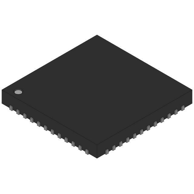
Space Saving Package: 48-pin 7-mm × 7-mm
QFN
The device simplicity (no software required), low
latency, and low power simplify the design of complex
systems. The DACs interface seamlessly with the
high-performance TRF370333 analog quadrature
modulator for direct upconversion architectures.
Digital data for both DAC channels is interleaved
through a single LVDS data bus with on-chip
termination. The high input rate of the devices allows
the processing of wide-bandwidth signals.
The devices are characterized for operation over the
entire industrial temperature range of –40°C to 85°C
and are available in a small 48-pin 7-mm × 7-mm
QFN package.
APPLICATIONS
•
•
•
•
Cellular Base Stations
Wideband Communications
Medical Instrumentation
Test and Measurement
The low power, small size, speed, superior crosstalk,
simplicity, and low latency of the DAC3152/DAC3162
make them an attractive fit for a variety of
applications.
ATEST
VFUSE
DVDD18
CLKVDD18
FUNCTIONAL BLOCK DIAGRAM
DACCLKP
LVPECL
Clock Distribution
1.2-V
Reference
DACCLKN
LVDS
IOUTAP
100
D11P
IOUTAN
12/10
IOUTBP
100
D0N
LVDS
DACA
De-interleave
D11N
D0P
BIASJ
DACB
IOUTBN
12/10
VREF
GND
SLEEPB
AVDD33
1
Please be aware that an important notice concerning availability, standard warranty, and use in critical applications of
Texas Instruments semiconductor products and disclaimers thereto appears at the end of this data sheet.
PRODUCTION DATA information is current as of publication date.
Products conform to specifications per the terms of the Texas
Instruments standard warranty. Production processing does not
necessarily include testing of all parameters.
Copyright © 2010–2012, Texas Instruments Incorporated
�DAC3152
DAC3162
SLAS736D – NOVEMBER 2010 – REVISED AUGUST 2012
www.ti.com
These devices have limited built-in ESD protection. The leads should be shorted together or the device placed in conductive foam
during storage or handling to prevent electrostatic damage to the MOS gates.
AVDD33
GND
IOUTBN
IOUTBP
39
38
37
41
40
BIASJ
DVDD18
42
CLKVDD18
AVDD33
AVDD33
43
GND
46
45
44
IOUTAP
IOUTAN
48
47
DAC3152 PINOUT AND PIN FUNCTIONS
DACCLKP
1
36
VFUSE
DACCLKN
2
35
ATEST
D9P
3
34
SLEEPB
D9N
4
33
DVDD18
D8P
5
32
NC
D8N
6
31
NC
D7P
7
D7N
8
DAC3152
RGZ Package
48-QFN 7x7mm
(Top View)
30
NC
29
NC
23
24
D0P
D0N
21
22
D1P
D1N
19
20
D2P
D2N
D4P
18
NC
VREF
25
17
12
D3N
NC
D5N
15
26
16
11
D3P
NC
D5P
DVDD18
NC
27
13
28
10
14
9
D4N
D6P
D6N
PIN FUNCTIONS
PIN
NAME
NO.
ATEST
I/O
DESCRIPTION
35
O
Factory use only. Leave unconnected for normal operation.
40, 43, 45
–
Analog supply voltage (3.3 V)
BIASJ
42
O
Full-scale output current bias. For 20-mA full-scale output current, connect a 960-Ω resistor to GND.
CLKVDD18
44
–
Internal clock buffer supply voltage (1.8 V)
This supply can be shared with DIGVDD18.
AVDD33
3, 5, 7, 9, 11, 13,
16, 19, 21, 23
D[9..0]P
I
LVDS positive-input data bits 0 through 9. Each positive/negative LVDS pair has an internal 100-Ω termination
resistor. Data format relative to DACCLKP/N clock is double data rate (DDR) with two data transfers per
DACCLKP/N clock cycle. Dual-channel data is interleaved on this bus.
D9P is most-significant data bit (MSB) – pin 3
D0P is least-significant data bit (LSB) – pin 23
4, 6, 8, 10, 12,
14, 17, 20, 22,
24
D[9..0]N
LVDS negative-input data bits 0 through 9. (See D[9:0]P description)
I
D9N is most-significant data bit (MSB) – pin 4
D0N is least-significant data bit (LSB) – pin 24
DACCLKP
1
I
Positive external LVPECL clock input with a self-bias of approximately CLKVDD18/2. Input data is latched on both
edges of DACCLKP/N (double data rate). The LVPECL clock signal should be AC coupled.
DACCLKN
2
I
Complementary external LVPECL clock input (see the DACCLKP description). The LVPECL clock signal should
be AC coupled.
15, 33, 41
–
Digital supply voltage (1.8 V). This supply can be shared with CLKVDD18.
39, 46,
Thermal pad
–
Pins 39 and 46 and the thermal pad located on the bottom of the QFN package are ground for all supplies.
IOUTAP
48
O
A-channel DAC current output. An offset binary data pattern of 0x0000 at the DAC input results in a full-scale
current sink and the least-positive voltage on the IOUTAP pin. Similarly, a 0x3FF data input results in a 0-mA
current sink and the most-positive voltage on the IOUTAP pin.
IOUTAN
47
O
A-channel DAC complementary current output. IOUTAN has the opposite behavior of the IOUTAP described for
IOUTAP. An input data value of 0x0000 results in a 0-mA sink and the most-positive voltage on the IOUTAN pin.
IOUTBP
37
O
B-channel DAC current output. See the IOUTAP description.
IOUTBN
38
O
B-channel DAC complementary current output. See the IOUTAN description.
25–32
–
No connect. Leave unconnected for normal operation.
SLEEPB
34
I
Connect to GND to put the device in sleep mode or to AVDD for active mode. Internal pullup
VFUSE
36
–
Digital supply voltage (1.8 V). This supply pin is also used for factory fuse programming. Connect to DVDD18
pins for normal operation.
VREF
18
I/O
DVDD18
GND
NC
2
Factory use only. Connect to a 0.1-μF decoupling capacitor to GND.
Submit Documentation Feedback
Copyright © 2010–2012, Texas Instruments Incorporated
Product Folder Links: DAC3152 DAC3162
�DAC3152
DAC3162
www.ti.com
SLAS736D – NOVEMBER 2010 – REVISED AUGUST 2012
AVDD33
GND
IOUTBN
IOUTBP
40
39
38
37
BIASJ
DVDD18
41
43
42
CLKVDD18
AVDD33
44
GND
AVDD33
46
45
IOUTAP
IOUTAN
48
47
DAC3162 PINOUT AND PIN FUNCTIONS
DACCLKP
1
36
VFUSE
DACCLKN
2
35
ATEST
D11P
3
34
SLEEPB
D11N
4
33
DVDD18
D10P
5
32
NC
D10N
6
31
NC
30
NC
D9P
7
D9N
8
D8P
DAC3162
RGZ Package
48-QFN 7x7mm
(Top View)
23
24
D2P
D2N
21
22
D3P
D3N
19
20
D4P
D6P
D4N
D1P
17
25
18
12
D5N
D1N
D7N
VREF
D0P
26
15
27
11
16
10
D7P
D5P
D8N
DVDD18
D0N
13
28
14
NC
9
D6N
29
PIN FUNCTIONS
PIN
NAME
ATEST
NO.
I/O
DESCRIPTION
35
O
Factory use only. Leave unconnected for normal operation.
40, 43, 45
–
Analog supply voltage (3.3 V)
BIASJ
42
O
Full-scale output current bias. For 20-mA full-scale output current, connect a 960-Ω resistor to GND.
CLKVDD18
44
–
Internal clock buffer supply voltage (1.8 V)
This supply can be shared with DIGVDD18.
AVDD33
D[11..0]P
3, 5, 7, 9, 11, 13,
16, 19, 21, 23,
25, 27
I
LVDS positive-input data bits 0 through 11. Each positive/negative LVDS pair has an internal 100-Ω termination
resistor. Data format relative to DACCLKP/N clock is double data rate (DDR) with two data transfers per
DACCLKP/N clock cycle. Dual channel data is interleaved on this bus.
D11P is most-significant data bit (MSB) – pin 3
D0P is least-significant data bit (LSB) – pin 27
D[11..0]N
4, 6, 8, 10, 12,
14, 17, 20, 22,
24, 26, 28
LVDS negative-input data bits 0 through 11. (See D[11:0]P description)
I
D11N is most-significant data bit (MSB) – pin 4
D0N is least-significant data bit (LSB) – pin 28
DACCLKP
1
I
Positive external LVPECL clock input with a self-bias of approximately CLKVDD18/2. Input data is latched on both
edges of DACCLKP/N (double data rate). The LVPECL clock signal should be AC coupled.
DACCLKN
2
I
Complementary external LVPECL clock input (see the DACCLKP description). The LVPECL clock signal should
be AC coupled.
15, 33, 41
–
Digital supply voltage (1.8 V)
This supply can be shared with CLKVDD18.
39, 46,
Thermal pad
–
Pins 39, 46 and the thermal pad located on the bottom of the QFN package are ground for all supplies.
IOUTAP
48
O
A-channel DAC current output. An offset binary data pattern of 0x0000 at the DAC input results in a full-scale
current sink and the least-positive voltage on the IOUTAP pin. Similarly, a 0xFFF data input results in a 0-mA
current sink and the most-positive voltage on the IOUTAP pin.
IOUTAN
47
O
A-channel DAC complementary current output. IOUTAN has the opposite behavior of the IOUTAP described for
IOUTAP. An input data value of 0x0000 results in a 0-mA sink and the most-positive voltage on the IOUTAN pin.
IOUTBP
37
O
B-channel DAC current output. See the IOUTAP description.
IOUTBN
38
O
B-channel DAC complementary current output. See the IOUTAN description.
25–32
–
No connect. Leave unconnected for normal operation.
SLEEPB
34
I
Connect to GND to put the device in sleep mode or to AVDD for active mode. Internal pullup.
VFUSE
36
–
Digital supply voltage (1.8 V). This supply pin is also used for factory fuse programming. Connect to DVDD18
pins for normal operation.
VREF
18
I/O
DVDD18
GND
NC
Factory use only. Connect to a 0.1-μF decoupling capacitor to GND.
Copyright © 2010–2012, Texas Instruments Incorporated
Product Folder Links: DAC3152 DAC3162
Submit Documentation Feedback
3
�DAC3152
DAC3162
SLAS736D – NOVEMBER 2010 – REVISED AUGUST 2012
www.ti.com
ABSOLUTE MAXIMUM RATINGS
over operating free-air temperature range (unless otherwise noted)
(1)
VALUE
MAX
–0.5
2.3
V
–0.5
2.3
V
AVDD33
–0.5
4
V
D[11..0]P/N
–0.5
DVDD18 + 0.5
V
DACCLKP/N
–0.5
CLKVDD18 + 0.5 V
V
BIASJ, SLEEPB
–0.5
AVDD33 + 0.7 V
V
–1
DVDD18, CLKVDD18
Supply-voltage range (2) VFUSE
Pin-voltage range (2)
UNIT
MIN
AVDD33 + 0.7 V
V
Peak input current (any input)
IOUTAP/N, IOUTBP/N
±20
mA
Peak total input current (all inputs)
±30
mA
Operating free-air temperature range, TA
–40
85
°C
Storage temperature range, Tstg
–65
150
°C
(1)
(2)
Stresses beyond those listed under Absolute Maximum Ratings may cause permanent damage to the device. These are stress ratings
only and functional operation of these or any other conditions beyond those indicated under Recommended Operating Conditions is not
implied. Exposure to absolute-maximum-rated conditions for extended periods may affect device reliability.
Measured with respect to GND
THERMAL INFORMATION
DAC3152
DAC3162
THERMAL METRIC (1) (2)
UNIT
RGZ (48 PINS)
θJA
Junction-to-ambient thermal resistance
28.9
θJCtop
Junction-to-case (top) thermal resistance
14.9
θJB
Junction-to-board thermal resistance
5.62
ψJT
Junction-to-top characterization parameter
0.3
ψJB
Junction-to-board characterization parameter
5.6
θJCbot
Junction-to-case (bottom) thermal resistance
1.7
(1)
(2)
4
°C/W
For more information about traditional and new thermal metrics, see the IC Package Thermal Metrics application report, SPRA953.
For thermal estimates of this device based on PCB copper area, see the TI PCB Thermal Calculator.
Submit Documentation Feedback
Copyright © 2010–2012, Texas Instruments Incorporated
Product Folder Links: DAC3152 DAC3162
�DAC3152
DAC3162
www.ti.com
SLAS736D – NOVEMBER 2010 – REVISED AUGUST 2012
ELECTRICAL CHARACTERISTICS – DC SPECIFICATION
DVDD18 = CLKVDD18 = 1.8 V, AVDD33 = 3.3 V, fDAC = 500 MSPS, fOUT = 1 MHz over recommended operating free-air
temperature range, IOUTFS = 20 mA (unless otherwise noted)
PARAMETER
TEST CONDITIONS
Resolution
DAC3152
MIN
TYP
DAC3162
MAX
10
MIN
TYP
UNIT
MAX
12
Bits
DC ACCURACY
DNL
Differential nonlinearity
INL
Integral nonlinearity
±0.1
±0.4
LSB
±0.15
±0.5
LSB
Gain error
±1.6
±1.6
%FSR
Gain mismatch
±0.2
±0.2
ANALOG OUTPUT (1)
Full-scale output current
Output compliance range
%FSR
2
20
2
20
AVDD
– 0.5
AVDD
+ 0.5
AVDD
– 0.5
AVDD
+ 0.5
Output resistance
Output capacitance
mA
V
300
300
kΩ
5
5
pF
REFERENCE
VREF
Internal reference voltage
1.14
1.2
1.26
1.14
1.2
1.26
V
TEMPERATURE COEFFICIENTS
Gain drift
±60
±60
ppm/°C
Reference-voltage drift
±41
±41
ppm/°C
POWER SUPPLY
AVDD33
CLKVDD18, DVDD18
PSRR
Power-supply rejection ratio
3
3.3
3.6
3
3.3
3.6
1.7
1.8
1.9
1.7
1.8
1.9
±0.1
V
V
DC tested
±0.1
%FSR/V
fDAC = 500 MSPS,
fOUT = 10 MHz
270
310
278
320
mW
16
23
17
25
mW
POWER CONSUMPTION
PDIS
Power dissipation
Power-down mode: no
clock, DAC on sleep
mode, static data pattern
I(AVDD33)
Analog supply current
55
65
56
65
mA
I(DVDD18)
I(CLKVDD)
Digital and clock supply current
50
55
53
63
mA
25
85
25
85
°C
Operating range
(1)
–40
–40
Measured differentially across IOUTAP/N or IOUTBP/N with 25 Ω each to AVDD.
Copyright © 2010–2012, Texas Instruments Incorporated
Product Folder Links: DAC3152 DAC3162
Submit Documentation Feedback
5
�DAC3152
DAC3162
SLAS736D – NOVEMBER 2010 – REVISED AUGUST 2012
www.ti.com
ELECTRICAL CHARACTERISTICS – DIGITAL SPECIFICATIONS
DVDD18 = CLKVDD18 = 1.8 V, AVDD33 = 3.3 V, fDAC = 500 MSPS, fOUT = 1 MHz over recommended operating free-air
temperature range, IOUTFS = 20 mA (unless otherwise noted)
PARAMETER
TEST CONDITIONS
DAC3152
MIN
TYP
150
400
DAC3162
MAX
MIN
TYP
150
400
MAX
UNIT
LVDS INPUTS: DIGITAL INPUT DATA (1)
VA,B+
Logic-high differential input voltage
threshold
VA,B–
Logic-low differential input voltage
threshold
VCOM
Input common mode
0.9
1.2
1.5
0.9
1.2
1.5
V
ZT
Internal termination
85
110
135
85
110
135
Ω
CL
LVDS input capacitance
fINTERL
Interleaved LVDS data rate
1000
1000
MSPS
fDATA
Input data rate (per DAC)
500
500
MSPS
–400
–150
–400
2
mV
–150
2
mV
pF
CLOCK INPUT: DACCLKP/N
Duty cycle
40%
Differential voltage
0.2
60%
1
Clock frequency
40%
0.2
60%
1
500
V
500
MHz
CMOS INTERFACE: SLEEPB
VIH
High-level input voltage
2
VIL
Low-level input voltage
IIH
High-level input current
-40
IIL
Low-level input current
-40
CI
CMOS Input capacitance
2
V
0.8
40
-40
40
-40
2
2
0.8
V
40
µA
40
µA
pF
DIGITAL INPUT DATA TIMING SPECIFICATIONS: DOUBLE EDGE LATCHING
ts(DATA)
Setup time, valid to either edge of
DACCLKP/N
200
200
ps
th(DATA)
Hold time, valid after either edge of
DACCLKP/N
200
200
ps
(1)
6
See LVDS INPUTS section for terminology.
Submit Documentation Feedback
Copyright © 2010–2012, Texas Instruments Incorporated
Product Folder Links: DAC3152 DAC3162
�DAC3152
DAC3162
www.ti.com
SLAS736D – NOVEMBER 2010 – REVISED AUGUST 2012
ELECTRICAL CHARACTERISTICS – AC SPECIFICATIONS
DVDD18 = CLKVDD18 = 1.8 V, AVDD33 = 3.3 V, fDAC = 500 MSPS, fOUT = 1 MHz over recommended operating free-air
temperature range, IOUTFS = 20mA (unless otherwise noted)
PARAMETER
ANALOG OUTPUT
fDAC
TEST CONDITIONS
TYP
DAC3162
MAX
MIN
TYP
UNIT
MAX
(1)
Maximum DAC rate
ts(DAC)
Output settling time to 0.1%
tr(IOUT)
tf(IOUT)
500
Transition: Code 0x0000 to
0xFFFF
500
MSPS
10
10
ns
Output rise time, 10% to 90%
220
220
ps
Output fall time, 90% to 10%
220
220
ps
1.5
1.5
DAC clock
cycles
Latency
Power-up
time
DAC3152
MIN
DAC wake-up time
IOUT current settling to
1% of IOUTFS.
2
2
μs
DAC sleep time
IOUT current settling to
less than 1% of IOUTFS.
2
2
μs
fDAC = 500 MSPS,
fOUT = 10 MHz
78
79
fDAC = 500 MSPS,
fOUT = 20 MHz
74
74
fDAC = 500 MSPS,
fOUT = 70 MHz
59
60
fDAC = 500 MSPS,
fOUT = 10 ± 0.5 MHz
91
93
fDAC = 500 MSPS,
fOUT = 20 ± 0.5 MHz
85
86
fDAC = 500 MSPS,
fOUT = 70 ± 0.5 MHz
62
62
500 MSPS,
10 MHz
–145
–155
500 MSPS,
70 MHz
–140
–140
fDAC = 491.52 MSPS,
fOUT = 30 MHz
68
76
fDAC = 491.52 MSPS,
fOUT = 70 MHz
67
70
AC PERFORMANCE (2)
SFDR
IMD3
Spurious-free dynamic range, single
tone at 0 dBFS
Third-order two-tone intermodulation
distortion, each tone at –12 dBFS
fDAC =
Noise spectral density, single tone at fOUT =
0 dBFS
fDAC =
fOUT =
NSD
ACLR (3)
Adjacent-channel leakage ratio,
single carrier
Channel isolation
(1)
(2)
(3)
fDAC = 500 MSPS,
fOUT = 10 MHz
dBc
dBc
dBc/Hz
dBc
90
90
dBc
Measured differentially across IOUTAP/N or IOUTBP/N with 25 Ω each to AVDD.
4:1 transformer output termination, 50-Ω doubly terminated load.
Single carrier, W-CDMA with 3.84 MHz BW, 5-MHz spacing, centered at IF, PAR = 12 dB. TESTMODEL 1, 10 ms
Copyright © 2010–2012, Texas Instruments Incorporated
Product Folder Links: DAC3152 DAC3162
Submit Documentation Feedback
7
�DAC3152
DAC3162
SLAS736D – NOVEMBER 2010 – REVISED AUGUST 2012
www.ti.com
Typical Characteristics
DVDD18 = CLKVDD18 = 1.8 V, AVDD33 = 3.3 V, fDAC = 500 MSPS, fOUT = 1 MHz, IOUTfs = 20 mA (unless otherwise noted)
100
Channel A
Channel B
Third Harmonic Distortion (dBc)
Second Harmonic Distortion (dBc)
90
80
70
60
70
60
50
0
50
fDAC = 500 MSPS
100
150
Output Frequency (MHz)
200
40
250
0
50
G001
Figure 1. DAC3152 Second-Harmonic Distortion vs
Frequency
100
150
Output Frequency (MHz)
200
250
G002
Figure 2. DAC3152 Third-Harmonic Distortion vs Frequency
0
80
Channel A
Channel B
fOUT =10 MHz
fDAC = 500 MSPS
−10
−20
70
Power (dBm)
Fifth Harmonic Distortion (dBc)
80
fDAC = 500 MSPS
50
60
−30
−40
−50
−60
−70
−80
fDAC = 500 MSPS
50
0
50
100
150
Output Frequency (MHz)
200
−90
250
50
G003
Figure 3. DAC3152 Fifth-Harmonic Distortion vs Frequency
100
150
Output Frequency (MHz)
200
250
G004
Figure 4. DAC3152 10-MHz Spectrum vs Frequency
0
80
fOUT =70 MHz
fDAC = 500 MSPS
−10
Channel A
Channel B
−20
70
−30
SFDR (dBc)
Power (dBm)
Channel A
Channel B
90
−40
−50
−60
60
50
−70
−80
−90
50
100
150
Output Frequency (MHz)
200
250
Submit Documentation Feedback
0
50
G005
Figure 5. DAC3152 70-MHz Spectrum vs Frequency
8
40
100
150
Output Frequency (MHz)
200
250
G000
Figure 6. DAC3152 Spurious-Free Dynamic Range
vs Frequency
Copyright © 2010–2012, Texas Instruments Incorporated
Product Folder Links: DAC3152 DAC3162
�DAC3152
DAC3162
www.ti.com
SLAS736D – NOVEMBER 2010 – REVISED AUGUST 2012
Typical Characteristics (continued)
DVDD18 = CLKVDD18 = 1.8 V, AVDD33 = 3.3 V, fDAC = 500 MSPS, fOUT = 1 MHz, IOUTfs = 20 mA (unless otherwise noted)
0
Channel A
Channel B
−125
−20
−130
−30
−135
−140
−145
−40
−50
−60
−70
−150
−80
−155
−90
fDAC = 500 MSPS
−160
fOUT = 10 MHz
Tone Spacing = 1 MHz
fDAC = 500 MSPS
−10
Power (dBm)
Noise Spectral Density (dBc/Hz)
−120
0
50
100
150
Output Frequency (MHz)
200
−100
250
5
7
G006
Figure 7. DAC3152 Noise Spectral Density
vs Frequency
9
11
Frequency (MHz)
13
15
G007
Figure 8. DAC3152 10-MHz Two-Tone Spectrum vs
Frequency
0
100
fOUT = 70 MHz
Tone Spacing = 1 MHz
fDAC = 500 MSPS
−10
−20
Channel A
Channel B
90
IMD3 (dBc)
Power (dBm)
−30
−40
−50
−60
80
70
−70
−80
60
−90
−100
65
67
69
71
Frequency (MHz)
73
50
75
Figure 9. DAC3152 70-MHz Two-Tone Spectrum vs
Frequency
100
G000
70
Alternate Channel ACLR (dB)
Channel A
Channel B
65
ACLR (dBc)
50
Output Frequency (MHz)
Figure 10. DAC3152 Intermodulation Distortion
vs Frequency
70
60
55
50
0
G008
fDAC = 491.52 MSPS
Test Model 1
Single Carrier
0
50
100
150
200
250
Channel A
Channel B
65
60
55
50
fDAC = 491.52 MSPS
Test Model 1
Single Carrier
0
50
100
150
200
G010
Figure 11. DAC3152 Alternate Channel vs Frequency
250
G011
Figure 12. DAC3152 Alternate Channel vs Frequency
Copyright © 2010–2012, Texas Instruments Incorporated
Product Folder Links: DAC3152 DAC3162
Submit Documentation Feedback
9
�DAC3152
DAC3162
SLAS736D – NOVEMBER 2010 – REVISED AUGUST 2012
www.ti.com
Typical Characteristics (continued)
DVDD18 = CLKVDD18 = 1.8 V, AVDD33 = 3.3 V, fDAC = 500 MSPS, fOUT = 1 MHz, IOUTfs = 20 mA (unless otherwise noted)
80
90
Second Harmonic Distortion (dBc)
Channel A
Channel B
SFDR (dBc)
70
60
50
40
0
50
100
150
Output Frequency (MHz)
200
80
70
60
fDAC = 500 MSPS
50
250
0
Fifth Harmonic Distortion (dBc)
80
70
60
50
G013
70
60
0
50
fDAC = 500 MSPS
100
150
Output Frequency (MHz)
200
50
250
0
50
G014
Figure 15. DAC3162 Third-Harmonic Distortion
vs Frequency
100
150
Output Frequency (MHz)
200
250
G015
Figure 16. DAC3162 Fifth-Harmonic Distortion vs Frequency
0
0
fOUT =10 MHz
fDAC = 500 MSPS
−10
−20
−20
−30
−30
−40
−50
−60
−40
−50
−60
−70
−70
−80
−80
50
100
150
Output Frequency (MHz)
200
250
−90
50
G016
Figure 17. DAC3162 10-MHz Spectrum vs Frequency
Submit Documentation Feedback
fOUT = 70 MHz
fDAC = 500 MSPS
−10
Power (dBm)
Power (dBm)
250
Channel A
Channel B
fDAC = 500 MSPS
10
200
80
Channel A
Channel B
90
−90
100
150
Output Frequency (MHz)
Figure 14. DAC3162 Second-Harmonic Distortion vs
Frequency
100
40
50
G012
Figure 13. DAC3162 Spurious-Free Dynamic Range
vs Frequency
Third Harmonic Distortion (dBc)
Channel A
Channel B
100
150
Output Frequency (MHz)
200
250
G017
Figure 18. DAC3162 70-MHz Spectrum vs Frequency
Copyright © 2010–2012, Texas Instruments Incorporated
Product Folder Links: DAC3152 DAC3162
�DAC3152
DAC3162
www.ti.com
SLAS736D – NOVEMBER 2010 – REVISED AUGUST 2012
Typical Characteristics (continued)
DVDD18 = CLKVDD18 = 1.8 V, AVDD33 = 3.3 V, fDAC = 500 MSPS, fOUT = 1 MHz, IOUTfs = 20 mA (unless otherwise noted)
100
−120
Channel A
Channel B
90
−130
NSD (dBc/Hz)
IMD3 (dBc)
Channel A
Channel B
−125
80
70
−135
−140
−145
−150
60
−155
fDAC = 500 MSPS
50
0
50
Output Frequency (MHz)
−160
100
Figure 19. DAC3152 Intermodulation Distortion
vs Frequency
−20
200
250
G018
fOUT = 70 MHz
Tone Spacing = 1 MHz
fDAC = 500 MSPS
−10
−20
−30
Power (dBm)
−30
Power (dBm)
100
150
Output Frequency (MHz)
0
fOUT = 10 MHz
Tone Spacing = 1 MHz
fDAC = 500 MSPS
−10
−40
−50
−60
−40
−50
−60
−70
−70
−80
−80
−90
−90
−100
−100
5
7
9
11
Frequency (MHz)
13
15
65
67
G019
Figure 21. DAC3162 10-MHz Two-Tone Spectrum
vs Frequency
69
71
Frequency (MHz)
73
75
G020
Figure 22. DAC3162 70-MHz Two-Tone Spectrum
vs Frequency
80
80
Alternate Channel ACLR (dB)
Channel A
Channel B
75
ACLR (dBc)
50
Figure 20. DAC3162 Noise Spectral Density vs Frequency
0
70
65
fDAC = 491.52 MSPS
Test Model 1
Single Carrier
60
55
0
G023
0
50
100
150
200
250
Channel A
Channel B
75
70
65
60
fDAC = 491.52 MSPS
Test Model 1
Single Carrier
0
50
100
150
200
G021
Figure 23. DAC3162 Alternate Channel vs Frequency
250
G022
Figure 24. DAC3162 Alternate Channel vs Frequency
Copyright © 2010–2012, Texas Instruments Incorporated
Product Folder Links: DAC3152 DAC3162
Submit Documentation Feedback
11
�DAC3152
DAC3162
SLAS736D – NOVEMBER 2010 – REVISED AUGUST 2012
www.ti.com
Typical Characteristics (continued)
DVDD18 = CLKVDD18 = 1.8 V, AVDD33 = 3.3 V, fDAC = 500 MSPS, fOUT = 1 MHz, IOUTfs = 20 mA (unless otherwise noted)
−20
−20
W-CDMA Test Model 1 at 30 MHz
−40
fOUT = 30 MHz
fDAC = 491.52 MSPS
−40
fOUT = 70 MHz
fDAC = 491.52 MSPS
−50
−60
−70
ACPR = 68.4 dBc
ALT1 = 68.7 dBc
−80
Power (dBm)
−50
Power (dBm)
W-CDMA Test Model 1 at 70 MHz
−30
−30
−60
−70
ACPR = 66.9 dBc
ALT1 = 67.4 dBc
−80
−90
−90
−100
−100
−110
−110
−120
−120
Frequency 2.55 MHz/div
Frequency 2.55 MHz/div
Figure 25. DAC3152 30-MHz WCDMA vs Frequency
Figure 26. DAC3152 70-MHz WCDMA vs Frequency
−20
−20
−40
Power (dBm)
−50
−60
−70
−80
−30
−40
W-CDMA Test Model 1 at 30 MHz
fOUT = 30 MHz
fDAC = 491.52 MSPS
−50
Power (dBm)
256-QAM at Baseline
fSYMBOL = 112 MHz
fDAC = 448 MSPS
Alpha = 0.12
RESBW = 30 kHz
−30
−60
−70
ACPR = 75.7 dBc
ALT1 = 76.2 dBc
−80
−90
−90
−100
−100
−110
−110
−120
−120
Frequency 22.4 MHz/div
Frequency 2.55 MHz/div
Figure 27. DAC3152 QAM vs Frequency
−20
Figure 28. DAC3162 30-MHz WCDMA vs Frequency
−20
W-CDMA Test Model 1 at 70 MHz
−40
fOUT = 70 MHz
fDAC = 491.52 MSPS
−40
−50
−60
−70
ACPR = 68.7 dBc
ALT1 = 70.4 dBc
−80
Power (dBm)
−50
Power (dBm)
256-QAM at Baseline
fSYMBOL = 112 MHz
fDAC = 448 MSPS
Alpha = 0.12
RESBW = 30 kHz
−30
−30
−60
−70
−80
−90
−90
−100
−100
−110
−110
−120
−120
Frequency 22.4 MHz/div
Frequency 2.55 MHz/div
Figure 29. DAC3162 70-MHz WCDMA vs Frequency
12
Submit Documentation Feedback
Figure 30. DAC3162 QAM vs Frequency
Copyright © 2010–2012, Texas Instruments Incorporated
Product Folder Links: DAC3152 DAC3162
�DAC3152
DAC3162
www.ti.com
SLAS736D – NOVEMBER 2010 – REVISED AUGUST 2012
Typical Characteristics (continued)
DVDD18 = CLKVDD18 = 1.8 V, AVDD33 = 3.3 V, fDAC = 500 MSPS, fOUT = 1 MHz, IOUTfs = 20 mA (unless otherwise noted)
300
dac3162
dac3152
Total Power (mW)
270
240
210
180
150
0
100
200
300
400
FDAC Frequency (MSPS)
500
600
G000
Figure 31. POWER vs Frequency
Copyright © 2010–2012, Texas Instruments Incorporated
Product Folder Links: DAC3152 DAC3162
Submit Documentation Feedback
13
�DAC3152
DAC3162
SLAS736D – NOVEMBER 2010 – REVISED AUGUST 2012
www.ti.com
APPLICATION INFORMATION
DATA INTERFACE
The parallel-port data interface to the device consists of a single LVDS bus that accepts interleaved A and B data
with up to 12-bit resolution. Data is sampled by the LVPECL double-data-rate (DDR) clock DACCLK. DACCLK is
additionally used for the data conversion process, and hence a low-jitter source is recommended. Setup and hold
requirements must be met for proper sampling.
The interleaved data for channels A and B is interleaved in the form A0, B0, A1, B1… into the data bus. Data into
the device is formatted according to the diagram shown in Figure 32.
Sample 0
DATA
A0
B0
Sample 1
A1
B1
A2
B2
Write B1 to DACB on
falling edge
A3
B3
A4
B4
A5
B5
ts(DATA)
A6
B6
A7
B7
A8
ts(DATA )
DACCLKP/N
(DDR)
th(DATA)
Write A 1 to DACA on rising
edge
th(DATA)
Figure 32. Data Transmission Format
14
Submit Documentation Feedback
Copyright © 2010–2012, Texas Instruments Incorporated
Product Folder Links: DAC3152 DAC3162
�DAC3152
DAC3162
www.ti.com
SLAS736D – NOVEMBER 2010 – REVISED AUGUST 2012
CLOCK INPUT
The DAC clock (DACCLKP/N) is an internally biased differential input that for optimal performance should be
driven by a low-jitter clock source. The DACCLK signal is used for both data latching (in DDR format) and as the
data conversion clock. Figure 33 shows an equivalent circuit for the DAC input clock.
CLKVDD
500 Ω
DACCLKP
Note: Input common mode level is
approximately 1/2 ´ CLKVDD18,
or 0.9 V nominal.
2 kΩ
2 kΩ
DACCLKN
500 Ω
GND
Figure 33. DACCLKP/N Equivalent Input Circuit
The preferred configuration for driving the DACCLK input consists of a differential ECL/PECL source as shown in
Figure 34. Although not optimal due to the limited signal swing, an LVDS source can also be used to drive the
clock input with the preferred configuration shown in Figure 35.
Differential ECL or
(LV)PECL Source
0.1 mF
DACCLKP
CAC
100 W
DACCLKN
0.1 mF
RPU
RPD
RPU and RPD are chosen
VTT
based on the clock driver
Figure 34. Clock Input Configuration LVPECL
Differential LVDS
Source
0.1 mF
DACCLKP
100 W
CAC
DACCLKN
0.1 mF
Figure 35. Clock Input Configuration LVDS
Copyright © 2010–2012, Texas Instruments Incorporated
Product Folder Links: DAC3152 DAC3162
Submit Documentation Feedback
15
�DAC3152
DAC3162
SLAS736D – NOVEMBER 2010 – REVISED AUGUST 2012
www.ti.com
A single-ended clock, such as a clean sinusoid or a 1.8 V LVCMOS signal (for low-rate operation), can also be
used to drive the clock if configured as in the input circuits of Figure 36 and Figure 37.
CAC
0.1 µF
1:4
DACCLKP
RT
200 Ω
Optional, may be bypassed
for sine-wave input
DACLCKN
Figure 36. Clock Input Configuration Using 50-Ω Cable Input
TTL/CMOS
source
Ropt
22 Ω
CAC
0.01 µF
Optional, reduces
clock feedthrough
1:1
DACCLKP
TTL/CMOS
source
DACLCKN
Ropt
22 Ω
DACCLKP
DACLCKN
0.01 µF
Figure 37. Clock Input Configuration With a Single-Ended TTL/CMOS Clock
16
Submit Documentation Feedback
Copyright © 2010–2012, Texas Instruments Incorporated
Product Folder Links: DAC3152 DAC3162
�DAC3152
DAC3162
www.ti.com
SLAS736D – NOVEMBER 2010 – REVISED AUGUST 2012
DATA INPUTS
The input data LVDS pairs (D[11:0]P/N) have the input configuration shown in Figure 38. Figure 39 shows the
typical input levels and common-mode voltage used to drive these inputs.
DVDD18
100 Ω
LVDS
Receiver
internal
digital in
GND
Figure 38. D[13:0]P/N LVDS Input Configuration
Example
DAC
LVDS
Receiver
100
VA,B
VA
1.4 V
VB
1V
400 mV
VA,B
0V
VA
VCOM =
(VA+VB)/2
–400 mV
VB
GND
1
Logical Bit
Equivalent
0
Figure 39. LVDS Data Input Levels
Table 1.
Applied Voltages
Resulting Differential
Voltage
Resulting
Common-Mode Voltage
VCOM
VA
VB
VA,B
1.4 V
1V
400 mV
1V
1.4 V
–400 mV
1.2 V
0.8 V
400 mV
0.8 V
1.2 V
–400 mV
1.2 V
1V
Logical Bit
Binary Equivalent
1
0
1
0
CMOS INPUT
Figure 40 shows a schematic of the SLEEPB equivalent CMOS digital inputs. See the specification table for logic
thresholds. The pullup circuitry is approximately equivalent to 100 kΩ.
AVDD33
100 kΩ
400 Ω
internal
digital in
SLEEPB
GND
Figure 40. SLEEPB Digital Equivalent Input
Copyright © 2010–2012, Texas Instruments Incorporated
Product Folder Links: DAC3152 DAC3162
Submit Documentation Feedback
17
�DAC3152
DAC3162
SLAS736D – NOVEMBER 2010 – REVISED AUGUST 2012
www.ti.com
REFERENCE OPERATION
The DAC3152/DAC3162 uses a band-gap reference and control amplifier for biasing the full-scale output current.
The full-scale output current is set by applying an external resistor RBIAS to pin BIASJ. The bias current IBIAS
through resistor RBIAS is defined by the on-chip band-gap reference voltage and control amplifier. The default fullscale output current equals 16 times this bias current and can thus be expressed as:
IOUTFS = 16 × IBIAS = 16 × VBG / RBIAS
The band-gap reference voltage delivers an accurate voltage of 1.2 V. The full-scale output current can be
adjusted from 20 mA down to 2 mA by varying resistor RBIAS. The internal control amplifier has a wide input
range, supporting the full-scale output current range of 20 dB. The recommended value for RBIAS is 960 Ω, which
results in a full-scale output current of 20 mA.
DAC TRANSFER FUNCTION
The DAC outputs of the DAC3152/DAC3162 consist of a segmented array of NMOS current sinks, capable of
sinking a full-scale output current up to 20 mA. Differential current switches direct the current to either one of the
complementary output nodes IOUTP or IOUTN. Complementary output currents enable differential operation,
thus canceling out common-mode noise sources (digital feed-through, on-chip and PCB noise), dc offsets, and
even-order distortion components, and increasing signal output power by a factor of four.
The full-scale output current is set using external resistor RBIAS in combination with an on-chip band-gap voltage
reference source (1.2 V) and control amplifier. Current IBIAS through resistor RBIAS is mirrored internally to provide
a maximum full-scale output current equal to 16 times IBIAS.
The relation between IOUTP and IOUTN can be expressed as:
IOUTFS = IOUTP + IOUTN
Current flowing into a node is denoted as – current, and current flowing out of a node as + current. Because the
output stage is a current sink, the current flows from AVDD33 into the IOUTP and IOUTN pins. The output
current flow in each pin driving a resistive load can be expressed as:
IOUTP = IOUTFS × ((2N – 1) – CODE) / 2N
IOUTN = IOUTFS × CODE / 2N
where CODE is the decimal representation of the DAC data input word and N is the DAC bit resolution.
For the case where IOUTP and IOUTN drive resistor loads RL directly, this translates into single-ended voltages
at IOUTP and IOUTN:
VOUTP = AVDD – | IOUTP | × RL
VOUTN = AVDD – | IOUTN | × RL
Assuming that the data is full scale (2N – 1 in offset binary notation) and the RL is 25 Ω, the differential voltage
between pins IOUTP and IOUTN can be expressed as:
VOUTP = AVDD – | – 0 mA | × 25 Ω = 3.3 V
VOUTN = AVDD – | –20 mA | × 25 Ω = 2.8 V
VDIFF = VOUTP – VOUTN = 0.5 V
Note that care should be taken not to exceed the compliance voltages at nodes IOUTP and IOUTN, which would
lead to increased signal distortion.
18
Submit Documentation Feedback
Copyright © 2010–2012, Texas Instruments Incorporated
Product Folder Links: DAC3152 DAC3162
�DAC3152
DAC3162
www.ti.com
SLAS736D – NOVEMBER 2010 – REVISED AUGUST 2012
ANALOG CURRENT OUTPUTS
The DAC outputs can be easily configured to drive a doubly terminated 50-Ω cable using a properly selected RF
transformer. Figure 41 and Figure 42 show the 50-Ω doubly terminated transformer configuration with 1:1 and 4:1
impedance ratios, respectively. Note that the center tap of the primary input of the transformer must be
connected to AVDD to enable a dc current flow. Applying a 20-mA full-scale output current leads to a 0.5-Vpp
output for a 1:1 transformer and a 1-Vpp output for a 4:1 transformer. The low dc impedance between IOUTP or
IOUTN and the transformer center tap sets the center of the ac signal to AVDD, so the 1-Vpp output for the 4:1
transformer results in an output between AVDD – 0.5 V and AVDD + 0.5 V.
AVDD (3.3V)
50 ?
1:1
IOUTP
RLOAD
100 ?
50 ?
IOUTN
50 ?
AVDD (3.3V)
Figure 41. Driving a Doubly Terminated 50-Ω Cable Using a 1:1 Impedance-Ratio Transformer
AVDD (3.3V)
100 ?
4:1
IOUTP
RLOAD
50 ?
IOUTN
100 ?
AVDD (3.3V)
Figure 42. Driving a Doubly Terminated 50-Ω Cable Using a 4:1 Impedance-Ratio Transformer
Copyright © 2010–2012, Texas Instruments Incorporated
Product Folder Links: DAC3152 DAC3162
Submit Documentation Feedback
19
�DAC3152
DAC3162
SLAS736D – NOVEMBER 2010 – REVISED AUGUST 2012
www.ti.com
PASSIVE INTERFACE TO ANALOG QUADRATURE MODULATORS
A common application in communication systems is to interface the DAC to an IQ modulator like the TRF3703
family of modulators from Texas Instruments. The input of the modulator is generally of high impedance and
requires a specific common-mode voltage. A simple resistive network can be used to maintain 50-Ω load
impedance for the DAC3152/DAC3162 and also provide the necessary common-mode voltages for both the DAC
and the modulator.
Vin ~ Varies
Vout ~ 2.8 to 3.8 V
I1
Signal Conditioning
IOUTAP
IOUTAN
IOUTBP
IOUTBN
I2
?
Q1
RF
Q2
Quadrature modulator
Figure 43. DAC3152/DAC3162 to Analog Quadrature Modulator Interface
The DAC3152/DAC3162 has a maximum 20-mA full-scale output and a voltage compliance range of AVDD ± 0.5
V. The TRF3703 IQ modulator family has three common-mode voltage options: 1.5 V, 1.7 V, and 3.3 V, and the
TRF370417 IQ modulator has a 1.7-V common mode.
Figure 44 shows the recommended passive network to interface the DAC to the TRF370317, which has a
common-mode voltage of 1.7 V. The network generates the 3.3-V common mode required by the DAC output
and 1.7 V at the modulator input, while still maintaining a 50-Ω load for the DAC.
V1
R1
I
R2
DAC3152/
DAC3162
I
R3
TRF370317/
TRF370417
V2
R3
R2
I
I
R1
V1
Figure 44. DAC3152/DAC3162 to TRF370317 or TRF370417 Interface
If V1 is set to 5 V and V2 is set to –5 V, the corresponding resistor values are R1 = 57 Ω, R2 = 80 Ω, and
R3 = 336 Ω. The loss developed through R2 is about –1.86 dB. When there is no –5-V supply available and V2
is set to 0 V, the resistor values are R1 = 66 Ω, R2 = 101 Ω, and R3 = 107 Ω. The loss with these values is
–5.76 dB.
Figure 45 shows the recommended network for interfacing with the TRF370333, which requires a common mode
of 3.3 V. This is the simplest interface, as there is no voltage shift. With V1 = 5 V and V2 = 0 V, the resistor
values are R1 = 66 Ω and R3 = 208 Ω.
20
Submit Documentation Feedback
Copyright © 2010–2012, Texas Instruments Incorporated
Product Folder Links: DAC3152 DAC3162
�DAC3152
DAC3162
www.ti.com
SLAS736D – NOVEMBER 2010 – REVISED AUGUST 2012
V1
R1
I
I
R3
DAC3152/
DAC3162
TRF370333
V2
R3
I
I
R1
V1
Figure 45. DAC3152/DAC3162 to TRF370333 Interface
In most applications, a baseband filter is required between the DAC and the modulator to eliminate the DAC
images. This filter can be placed after the common-mode biasing network. For the DAC-to-modulator network
shown in Figure 46, R2 and the filter load R4 must be considered into the DAC impedance. The filter must be
designed for the source impedance created by the resistor combination of R3 || (R2 + R1). The effective
impedance seen by the DAC is affected by the filter termination resistor, resulting in R1 || (R2 + R3 || (R4/2)).
V1
R1
R2
I
R3
DAC3152/
DAC3162
V2
Filter
R4
R3
I
TRF370333/
TRF370317/
TRF370417
R2
R1
V1
Figure 46. DAC to Modulator Interface With Filter
Factoring in R4 into the DAC load, a typical interface to the TRF370317 with V1 = 5 V and V2 = 0 V results in the
following values: R1 = 72 Ω, R2 = 116 Ω, R3 = 124 Ω and R4 = 150 Ω. This implies that the filter must be
designed for 75-Ω input and output impedance (single-ended impedance). The common-mode levels for the DAC
and modulator are maintained at 3.3 V and 1.7 V, and the DAC load is 50 Ω. The added load of the filter
termination causes the signal to be attenuated by –10.8 dB.
A filter can be implemented in a similar manner to interface with the TRF370333. In this case, it is much simpler
to balance the loads and common-mode voltages, due to the absence of R2. An added benefit is that there is no
loss in this network. With V1 = 5 V and V2 = 0 V, the network can be designed such that R1 = 115 Ω,
R3 = 681 Ω, and R4 = 200 Ω. This results in a filter impedance of R1 || R2 = 100 Ω, and a DAC load of R1 || R3
|| (R4/2), which is equal to 50 Ω. R4 is a differential resistor and does not affect the common-mode level created
by R1 and R3. The common-mode voltage is set at 3.3 V for a full-scale current of 20 mA.
For more information on how to interface the DAC3152/DAC3162 to an analog quadrature modulator, see the
application reports Passive Terminations for Current Output DACs (SLAA399) and Design of Differential Filters
for High-Speed Signal Chains (SLWA053).
Copyright © 2010–2012, Texas Instruments Incorporated
Product Folder Links: DAC3152 DAC3162
Submit Documentation Feedback
21
�DAC3152
DAC3162
SLAS736D – NOVEMBER 2010 – REVISED AUGUST 2012
www.ti.com
POWER-UP SEQUENCE
The following start-up sequence is recommended to power up the DAC3152/DAC3162:
• Supply 1.8 V to DVDD18 and CLKVDD18 simultaneously, and 3.3 V to AVDD33. Within AVDD33, the
multiple AVDD33 pins should be powered up simultaneously. The 1.8-V and 3.3-V supplies can be powered
up simultaneously or in any order.
There are no specific requirements on the ramp rate for the supplies.
• Provide the DAC clock to the DACCLKP/N inputs.
• Toggle the SLEEPB pin for a minimum 25-ns low pulse duration.
• Provide the LVDS data inputs.
DEFINITION OF SPECIFICATIONS
Adjacent-Carrier Leakage Ratio (ACLR): Defined for a 3.84-Mcps 3GPP W-CDMA input signal measured in a
3.84-MHz bandwidth at a 5-MHz offset from the carrier with a 12-dB peak-to-average ratio.
Analog and Digital Power-Supply Rejection Ratio (APSRR, DPSRR): Defined as the percentage error in the
ratio of the delta IOUT and delta supply voltage normalized with respect to the ideal IOUT current.
Differential Nonlinearity (DNL): Defined as the variation in analog output associated with an ideal 1-LSB
change in the digital input code.
Gain Drift: Defined as the maximum change in gain, in terms of ppm of full-scale range (FSR) per °C, from the
value at ambient (25°C) to values over the full operating temperature range.
Gain Error: Defined as the percentage error (in FSR%) for the ratio between the measured full-scale output
current and the ideal full-scale output current.
Integral Nonlinearity (INL): Defined as the maximum deviation of the actual analog output from the ideal output,
determined by a straight line drawn from zero scale to full scale.
Intermodulation Distortion (IMD3): The two-tone IMD3 is defined as the ratio (in dBc) of the third-order
intermodulation distortion product to either fundamental output tone.
Offset Drift: Defined as the maximum change in dc offset, in terms of ppm of full-scale range (FSR) per °C, from
the value at ambient (25°C) to values over the full operating temperature range.
Offset Error: Defined as the percentage error (in FSR%) for the ratio between the measured mid-scale output
current and the ideal mid-scale output current.
Output Compliance Range: Defined as the minimum and maximum allowable voltage at the output of the
current-output DAC. Exceeding this limit may result in reduced reliability of the device or adversely affecting
distortion performance.
Reference Voltage Drift: Defined as the maximum change of the reference voltage in ppm per degree Celsius
from the value at ambient (25°C) to values over the full operating temperature range.
Noise Spectral Density (NSD): Defined as the difference of power (in dBc) between the output tone signal
power and the noise floor of 1 Hz bandwidth within the first Nyquist zone, excluding harmonics.
Signal-to-Noise Ratio (SNR): Defined as the ratio of the rms value of the fundamental output signal to the RMS
sum of all other spectral components below the Nyquist frequency, including noise, but excluding the first six
harmonics and dc.
22
Submit Documentation Feedback
Copyright © 2010–2012, Texas Instruments Incorporated
Product Folder Links: DAC3152 DAC3162
�DAC3152
DAC3162
www.ti.com
SLAS736D – NOVEMBER 2010 – REVISED AUGUST 2012
REVISION HISTORY
Changes from Original (November 2010) to Revision A
•
Page
Deleted the DAC3172 device ............................................................................................................................................... 1
Changes from Revision A (November 2010) to Revision B
Page
•
Changed Feature bullet From: High DC Accuracy: ±1 LSB DNL, ±2 LSB INL To: High DC Accuracy: ±0.25 LSB DNL
(10-bit), ± 0.5 LSB INL (12-bit) ............................................................................................................................................. 1
•
Added text "The LVPECL clock signal should be AC coupled" to Pin DACCLKP and DACCLKN descriptions. ................. 2
•
Added text "The LVPECL clock signal should be AC coupled" to Pin DACCLKP and DACCLKN descriptions. ................. 3
•
Added values to the Thermal Information table .................................................................................................................... 4
•
Changed the ELECTRICAL CHARACTERISTICS – DC SPECIFICATION table ................................................................ 5
•
Added Min and Max values to VCOM - Internal common mode ............................................................................................. 6
•
Added Min and Max values to ZT - Internal termination ....................................................................................................... 6
•
Changed the AC Performance Typical values for DAC3152 and DAC3162 ........................................................................ 7
•
Added the Typical Characteristics section ............................................................................................................................ 8
•
Replaced Signal to Noise Ratio (SNR) with Noise Spectral Density (NSD) ....................................................................... 22
Changes from Revision B (December 2011) to Revision C
Page
•
Changed the CLOCK INPUT: DACCLKP/N - Differential voltage MIN value From: 0.4V To: 0.2V for both devices .......... 6
•
Deleted Note 2 From the DIGITAL SPECIFICATIONS table- Driving the clock input with a differential voltage lower
than 1 V results in degraded performance. .......................................................................................................................... 6
Changes from Revision C (February 2012) to Revision D
Page
•
Added Figure 31 ................................................................................................................................................................. 12
•
Changed Figure 34 ............................................................................................................................................................. 15
•
Added Figure 35 ................................................................................................................................................................. 15
•
Moved the DEFINITION OF SPECIFICATIONS to the end of the data sheet ................................................................... 22
Copyright © 2010–2012, Texas Instruments Incorporated
Product Folder Links: DAC3152 DAC3162
Submit Documentation Feedback
23
�PACKAGE OPTION ADDENDUM
www.ti.com
10-Dec-2020
PACKAGING INFORMATION
Orderable Device
Status
(1)
Package Type Package Pins Package
Drawing
Qty
Eco Plan
(2)
Lead finish/
Ball material
MSL Peak Temp
Op Temp (°C)
Device Marking
(3)
(4/5)
(6)
DAC3152IRGZR
ACTIVE
VQFN
RGZ
48
2500
RoHS & Green
NIPDAU
Level-3-260C-168 HR
-40 to 85
DAC3152I
DAC3152IRGZT
ACTIVE
VQFN
RGZ
48
250
RoHS & Green
NIPDAU
Level-3-260C-168 HR
-40 to 85
DAC3152I
DAC3162IRGZR
ACTIVE
VQFN
RGZ
48
2500
RoHS & Green
NIPDAU
Level-3-260C-168 HR
-40 to 85
DAC3162I
DAC3162IRGZT
ACTIVE
VQFN
RGZ
48
250
RoHS & Green
NIPDAU
Level-3-260C-168 HR
-40 to 85
DAC3162I
(1)
The marketing status values are defined as follows:
ACTIVE: Product device recommended for new designs.
LIFEBUY: TI has announced that the device will be discontinued, and a lifetime-buy period is in effect.
NRND: Not recommended for new designs. Device is in production to support existing customers, but TI does not recommend using this part in a new design.
PREVIEW: Device has been announced but is not in production. Samples may or may not be available.
OBSOLETE: TI has discontinued the production of the device.
(2)
RoHS: TI defines "RoHS" to mean semiconductor products that are compliant with the current EU RoHS requirements for all 10 RoHS substances, including the requirement that RoHS substance
do not exceed 0.1% by weight in homogeneous materials. Where designed to be soldered at high temperatures, "RoHS" products are suitable for use in specified lead-free processes. TI may
reference these types of products as "Pb-Free".
RoHS Exempt: TI defines "RoHS Exempt" to mean products that contain lead but are compliant with EU RoHS pursuant to a specific EU RoHS exemption.
Green: TI defines "Green" to mean the content of Chlorine (Cl) and Bromine (Br) based flame retardants meet JS709B low halogen requirements of


 工商网监
湘ICP备2023018690号
工商网监
湘ICP备2023018690号
