�������
SLAS352C − DECEMBER 2001 − REVISED AUGUST 2004
��
��
��� ����
DIGITAL-TO-ANALOG CONVERTER
FEATURES
D 400-MSPS Update Rate
D LVDS-Compatible Input Interface
D Spurious Free Dynamic Range (SFDR) to
D
D
D
D
D
D
Nyquist
− 69 dBc at 70-MHz IF, 400 MSPS
W-CDMA Adjacent Channel Power Ratio
ACPR
− 73 dBc at 30.72-MHz IF, 122.88 MSPS
− 71 dBc at 61.44-MHz IF, 245.76 MSPS
Differential Scalable Current Outputs: 2 mA to
20 mA
On-Chip 1.2-V Reference
Single 3.3-V Supply Operation
Power Dissipation: 820 at fclk = 400 MSPS,
fout = 70 MHz
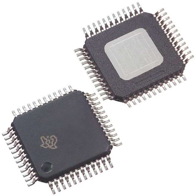
Package: 48-Pin HTQFP PowerPad,
TJA = 28.8°C/W
APPLICATIONS
D Cellular Base Transceiver Station Transmit
D
D
D
DESCRIPTION
Channel
− CDMA: WCDMA, CDMA2000, IS−95
− TDMA: GSM, IS−136, EDGE/GPRS
− Supports Single-Carrier and Multicarrier
Applications
Test and Measurement: Arbitrary Waveform
Generation
Direct Digital Synthesis (DDS)
Cable Modem Headend
The DAC5675 is a 14-bit resolution high-speed
digital-to-analog converter. The DAC5675 is designed
for high-speed digital data transmission in wired and
wireless communication systems, high-frequency
direct-digital synthesis (DDS), and waveform
reconstruction in test and measurement applications.
The DAC5675 has excellent spurious free dynamic
range (SFDR) at high intermediate frequencies, which
makes the DAC5675 well suited for multicarrier
transmission in TDMA and CDMA based cellular base
transceiver stations BTS.
The DAC5675 operates from a single-supply voltage of
3.3 V. Power dissipation is 820 mW at fclk = 400 MSPS,
fout = 70 MHz. The DAC5675 provides a nominal
full-scale differential current output of 20 mA,
supporting both single-ended and differential
applications. The output current can be directly fed to
the load with no additional external output buffer
required. The output is referred to the analog supply
voltage AVDD.
The DAC5675 is manufactured on Texas Instruments
advanced high-speed mixed-signal BiCMOS process.
The DAC5675 comprises a LVDS (low-voltage
differential signaling) interface. LVDS features a low
differential voltage swing with a low constant power
consumption across frequency, allowing for high speed
data transmission with low noise levels, i.e., low
electromagnetic interference (EMI). LVDS is typically
implemented in low-voltage digital CMOS processes,
making it the ideal technology for high-speed interfacing
between the DAC5675 and high-speed low-voltage
CMOS ASICs or FPGAs. The DAC5675 currentsource-array architecture supports update rates of up to
400 MSPS. On-chip edge-triggered input latches
provide for minimum setup and hold times thereby
relaxing interface timing.
Please be aware that an important notice concerning availability, standard warranty, and use in critical applications of
Texas Instruments semiconductor products and disclaimers thereto appears at the end of this data sheet.
PowerPAD is a trademark of Texas Instruments. All other trademarks are the property of their respective owners.
���������� ���� ����������� �� �!��"�� �� �� #!$%������� &��"'
���&!��� ������� �� �#"����������� #"� �(" �"��� �� �")�� �����!�"���
����&��& *������+' ���&!����� #���"����, &�"� ��� �"�"�����%+ ���%!&"
�"����, �� �%% #����"�"��'
Copyright 2002 − 2004, Texas Instruments Incorporated
www.ti.com
1
��������
SLAS352C − DECEMBER 2001 − REVISED AUGUST 2004
DESCRIPTION (continued)
The DAC5675 has been specifically designed for a differential transformer coupled output with a 50-Ω doubly
terminated load. With the 20-mA full-scale output current, both a 4:1 impedance ratio (resulting in an output
power of 4 dBm) and 1:1 impedance ratio transformer (-2 dBm) is supported. The last configuration is preferred
for optimum performance at high output frequencies and update rates. The output voltage compliance ranges
from 2.15 V to AVDD + 0.03 V.
An accurate on-chip 1.2-V temperature compensated bandgap reference and control amplifier allows the user
to adjust this output current from 20 mA down to 2 mA. This provides 20-dB gain range control capabilities.
Alternatively, an external reference voltage may be applied. The DAC5675 features a SLEEP mode, which
reduces the standby power to approximately 150 mW.
The DAC5675 is available in a 48-pin HTQFP thermally enhanced PowerPad package. This package increases
thermal efficiency in a standard size IC package. The device is characterized for operation over the industrial
temperature range of −40°C to 85°C.
AVDD
AGND
AGND
AVDD
IOUT2
IOUT1
AVDD
AGND
EXTIO
BIASJ
DLLOFF
SLEEP
PHP PACKAGE
(TOP VIEW)
48 47 46 45 44 43 42 41 40 39 38 37
D13A
D13B
D12A
D12B
D11A
D11B
D10A
D10B
D9A
D9B
D8A
D8B
1
36
2
35
3
34
4
33
5
32
6
31
7
30
8
29
9
28
10
27
11
26
25
12
D0B
D0A
D1B
D1A
D2B
D2A
D3B
D3A
D4B
D4A
D5B
D5A
D7A
D7B
DVDD
DGND
DVDD
DGND
AGND
AVDD
CLKC
CLK
D6A
D6B
13 14 15 16 17 18 19 20 21 22 23 24
AVAILABLE OPTIONS
PACKAGED DEVICE
TA
48-HTQFP PowerPAD PLASTIC QUAD FLATPACK
DAC5675IPHP
−40°C to 85°C
2
DAC5675IPHPR
www.ti.com
��������
SLAS352C − DECEMBER 2001 − REVISED AUGUST 2004
functional block diagram
SLEEP
DAC5675
Bandgap
Reference
1.2 V
IOUT1
−
EXTIO
Current
Source
Array
+
BIASJ
IBIAS
Output
Current
Switches
IOUT2
Control Amp
14
LVDS
Input
Interface
D[13:0]A
D[13:0]B
Input
Latches
Decoder
DAC
Latch
+
Drivers
14
CLK
+
CLKC
−
DLL
AVDD(4x)
AGND(4x)
DVDD(2x)
www.ti.com
DLLOFF
DGND(2x)
3
��������
SLAS352C − DECEMBER 2001 − REVISED AUGUST 2004
Terminal Functions
TERMINAL
NAME
NO.
AGND
19, 41, 46, 47
AVDD
BIASJ
I/O
DESCRIPTION
I
Analog negative supply voltage (ground)
20, 42, 45, 48
I
Analog positive supply voltage
39
O
Full-scale output current bias
CLK
22
I
External clock input
CLKC
21
I
Complementary external clock input
D[13..0]A
1, 3, 5, 7, 9, 11,
13, 23, 25, 27,
29, 31, 33, 35
I
LVDS positive input, data bits 0 through 13
D13A is most significant data bit (MSB)
D0A is least significant data bit (MSB)
D[13..0]B
2, 4, 6, 8, 10, 12,
14, 24, 26, 28,
30, 32, 34, 36
I
LVDS negative input, data bits 0 through 13
D13B is most significant data bit (MSB)
D0B is least significant data bit (MSB)
DGND
16, 18
I
Digital negative supply voltage (ground)
DLLOFF
38
I
High DLL off / Low = DLL on
DVDD
15, 17
I
Digital positive supply voltage
EXTIO
40
I/O
Internal reference output or external reference input. Requires a 0.1-µF decoupling capacitor to AGND
when used as reference output.
IOUT1
43
O
DAC current output. Full scale when all input bits are set 1. Connect reference side of DAC load
resistors to AVDD
IOUT2
44
O
DAC complementary current output. Full scale when all input bits are 0. Connect reference side of DAC
load resistors to AVDD
SLEEP
37
I
Asynchronous hardware power down input. Active high. No pull down or pull up.
Must be asserted high or low.
4
www.ti.com
��������
SLAS352C − DECEMBER 2001 − REVISED AUGUST 2004
detailed description
Figure 1 shows a simplified block diagram of the current steering DAC5675. The DAC5675 consists of a
segmented array of non-transistor current sources, capable of delivering a full-scale output current up to 20 mA.
Differential current switches direct the current of each current source to either one of the complementary output
nodes IOUT1 or IOUT2. The complementary current output thus enables differential operation, canceling out
common mode noise sources (digital feed-through, on-chip and PCB noise), dc offsets, even order distortion
components, thereby doubling signal output power.
The full-scale output current is set using an external resistor (RBIAS) in combination with an on-chip bandgap
voltage reference source (1.2 V) and control amplifier. The current (IBIAS) through resistor RBIAS is mirrored
internally to provide a full-scale output current equal to 16 times IBIAS. The full-scale current is adjustable from
20 mA down to 2 mA by using the appropriate bias resistor value.
SLEEP
3.3 V
(AVDD)
DAC5675
Bandgap
Reference
1.2 V
50 Ω
1:1
IOUT1
EXTIO
CEXT
0.1 µF
RBIAS
1 kΩ
−
BIASJ
Current
Source
Array
+
RLOAD
50 Ω
100 Ω
IOUT2
Control Amp
IBIAS
0.1 µF
Output
Current
Switches
50 Ω
1 kΩ
LVDS
Input
Interface
D[13:0]B
Input
Latches
Decoder
3.3 V
(AVDD)
3.3 V
(AVDD)
14
D[13:0]A
Output
DAC
Latch
+
Drivers
14
1:4
Clock
Input
CLK
RT
200 Ω
CLKC
+
DLL
DLLOFF
−
AVDD(4x)
AGND(4x)
3.3 V
DVDD(2x)
DGND(2x)
3.3 V
Figure 1. Application Schematic
www.ti.com
5
��������
SLAS352C − DECEMBER 2001 − REVISED AUGUST 2004
detailed description (continued)
digital inputs
The DAC5675 comprises a low voltage differential signaling (LVDS) bus input interface. The LVDS features a
low differential voltage swing with low constant power consumption (~4 mA per complementary data input)
across frequency. The differential characteristic of LVDS allows for high-speed data transmission with low
electromagnetic interference (EMI) levels. The LVDS input minimum and maximum input threshold table lists
the LVDS input levels. Figure 2 shows the equivalent complementary digital input interface for the DAC5675,
valid for pins D[13..0]A and D[13..0]B. Note that the LVDS interface features internal 110-Ω resistors for proper
termination. Figure 3 shows the LVDS input timing measurement circuit and waveforms. A common mode level
of 1.2 V and a differential input swing of 0.8 V is applied to the inputs.
AVDD
DAC5675
DAC5675
D[13:0]A
100-Ω
Termination
Resistor
Internal
Digital In
D[13:0]B
D[13:0]A
D[13:0]B
Internal
Digital In
AGND
Figure 2. LVDS Digital Equivalent Input
AVDD
DAC5675
VA
1.4 V
VB
1V
VA,B
VA,B
0.4 V
0V
V COM +
VA ) VB
2
VA
−0.4 V
VB
Logical Bit
Equivalent
AGND
Figure 3. LVDS Timing Test Circuit and Input Test Levels
6
www.ti.com
1
0
��������
SLAS352C − DECEMBER 2001 − REVISED AUGUST 2004
digital inputs (continued)
Figure 4 shows a schematic of the equivalent CMOS/TTL-compatible digital inputs of the DAC5675, valid for
pins SLEEP and DLLOFF.
DVDD
DAC5675
Internal
Digital In
Digital Input
DGND
Figure 4. CMOS/TTL Digital Equivalent Input
clock input and timing
The DAC5675 comprises a delay locked loop DLL for internal clock alignment. Enabling the DLL is controlled
by pin DLLOFF. The DLL should be enabled for update rates in excess of 100 MSPS. The DLL works only to
maximize setup and hold times of the digital input and does not affect the analog output of the DAC. Figure 5
shows the clock and data input timing diagram. The DAC5675 features a differential clock input. Internal
edge-triggered flip-flops latch the input word on the rising edge of the positive clock input CLK (falling edge of
the negative/complementary clock input CLKC). The DAC core is updated with the data word on the following
rising edge of the positive clock input CLK (falling edge of CLKC). This results in a conversion latency of one
clock cycle. The DAC5675 provides for minimum setup and hold times (>0.25 ns), allowing for noncritical
external interface timing. The clock duty cycle can be chosen arbitrarily under the timing constraints listed in
the electrical characteristics section. However, a 50% duty cycle gives the optimum dynamic performance.
The DAC5675 clock input can be driven by a differential sine wave. The ac coupling, in combination with internal
biasing ensures that the sine wave input is centered at the optimum common-mode voltage that is required for
the internal clock buffer. The DAC5675 clock input can also be driven single-ended, this is shown in Figure 6.
The best SFDR performance is typically achieved by driving the inputs differentially.
www.ti.com
7
��������
SLAS352C − DECEMBER 2001 − REVISED AUGUST 2004
clock input and timing (continued)
D[13:0]A
Valid Data
D[13:0]B
th(D)
tsu(D)
tw(H)
td(D) = 1/fCLK
CLK
CLKC
50%
50%
50%
50%
50%
tw(L)
ts(DAC)
tpd
0.1%
DAC Output
IOUT1/IOUT2
90%
50%
10%
0.1%
tr(IOUT)
Figure 5. Timing Diagram
AVDD
DAC5675
R1
1 kΩ
Internal
Digital In
R1
1 kΩ
CLK
CLKC
R2
2 kΩ
R2
2 kΩ
AGND
Optional, May Be Bypassed
Swing Limitation
DAC5675
CAC
0.1 µF
1:4
CLK
RT
200 Ω
CLKC
Termination Resistor
Figure 6. Clock Equivalent Input
8
www.ti.com
��������
SLAS352C − DECEMBER 2001 − REVISED AUGUST 2004
clock input and timing (continued)
Figure 7 shows the equivalent schematic of the differential clock input buffer. The input nodes are internally
self-biased enabling ac coupling of the clock inputs. Figure 8 shows the preferred configuration for driving the
DAC5675.
DAC5675
Ropt
22 Ω
TTL/CMOS Source
CLK
CLKC
0.01 µF
Node CLKC
Internally Biased
Figure 7. Driving the DAC5675 With a Single-Ended TTL/CMOS Clock Source
DAC5675
CAC
0.01 µF
Differential
ECL
or
(LV)PECL
Source
+
CLK
CAC
0.01 µF
−
CLKC
RT
50 Ω
RT
50 Ω
VTT
Figure 8. Driving the DAC5675 With a Differential ECL/PECL Clock Source
Single-Ended
ECL
or
(LV)PECL
Source
ECL/PECL
Gate
DAC5675
CAC
0.01 µF
CLK
CAC
0.01 µF
CLKC
RT
50 Ω
RT
50 Ω
VTT
Figure 9. Driving the DAC5675 With a Single-Ended ECL/PECL Clock Source
www.ti.com
9
��������
SLAS352C − DECEMBER 2001 − REVISED AUGUST 2004
detailed description (continued)
supply inputs
The DAC5675 comprises separate analog and digital supplies, i.e., AVDD and DVDD respectively. These supply
inputs can be set independently from 3.6 V down to 3.15 V.
DAC transfer function
The DAC5675 delivers complementary output currents IOUT1 and IOUT2. The DAC supports straight binary
coding, with D13 being the MSB and D0 the LSB (For ease of notation we denote D13..D10 as the logical bit
equivalent of the complementary LVDS inputs D[13..0]A and D[13..0]B). Output current IOUT1 equals the
approximate full-scale output current when all input bits are set high, i.e., the binary input word has the decimal
representation 16383. Full-scale output current flows through terminal IOUT2 when all input bits are set low
(mode 0, straight binary input). The relation between IOUT1 and IOUT2 can thus be expressed as:
IOUT1 = IO(FS) – IOUT2
where IO(FS) is the full-scale output current. The output currents can be expressed as:
I
IOUT1 +
CODE
O(FS)
16384
I
IOUT2 +
O(FS)
(16383–CODE)
16384
where CODE is the decimal representation of the DAC data input word. Output currents IOUT1 and IOUT2 drive
a load RL. RL is the combined impedance for the termination resistance and/or transformer load resistance,
RLOAD (see Figures 11 and 12). This would translate into single-ended voltages VOUT1 and VOUT2 at terminal
IOUT1 and IOUT2, respectively, of:
CODE
VOUT1 + IOUT1
R +
L
VOUT2 + IOUT2
R +
L
I
O(FS)
16384
R
(16383 * CODE)
I
L
O(FS)
R
L
16384
The differential output voltage VOUT(DIFF) can thus be expressed as:
VOUT
(DIFF)
+ VOUT1 * VOUT2 +
(2CODE * 16383)
I
O(FS)
R
L
16384
The latter equation shows that applying the differential output results in doubling of the signal power delivered
to the load. Since the output currents IOUT1 and IOUT2 are complementary, they become additive when
processed differentially. Note that care should be taken not to exceed the compliance voltages at node IOUT1
and IOUT2, which leads to increased signal distortion.
10
www.ti.com
��������
SLAS352C − DECEMBER 2001 − REVISED AUGUST 2004
detailed description (continued)
reference operation
The DAC5675 comprises a bandgap reference and control amplifier for biasing the full-scale output current. The
full-scale output current is set by applying an external resistor RBIAS. The bias current IBIAS through resistor
RBIAS is defined by the on-chip bandgap reference voltage and control amplifier. The full-scale output current
equals 16 times this bias current. The full-scale output current IO(FS) is thus expressed as:
I
O(FS)
+ 16
I
BIAS
+
16
V
R
EXTIO
BIAS
where VEXTIO is the voltage at terminal EXTIO. The bandgap reference voltage delivers an accurate voltage
of 1.2 V. This reference can be override by applying a external voltage to terminal EXTIO. The bandgap
reference can additionally be used for external reference operation. In that case, an external buffer with high
impedance input should be applied in order to limit the bandgap load current to a maximum of 100 nA. The
capacitor CEXT may be omitted. Terminal EXTIO serves as either a input or output node. The full-scale output
current is adjustable from 20 mA down to 2 mA by varying resistor RBIAS.
analog current outputs
Figure 10 shows a simplified schematic of the current source array output with corresponding switches.
Differential non switches direct the current of each individual PMOS current source to either the positive output
node IOUT1 or its complementary negative output node IOUT2. The output impedance is determined by the
stack of the current sources and differential switches, and is >300 kΩ in parallel with an output capacitance of
5 pF.
The external output resistors are referred to the positive supply AVDD.
3.3 V
(AVDD)
RLOAD
RLOAD
IOUT2
IOUT1
S(1)
S(1)C
S(2)
S(2)C
S(N)
S(N)C
Current Source Array
DAC5675
AGND
Figure 10. Equivalent Analog Current Output
www.ti.com
11
��������
SLAS352C − DECEMBER 2001 − REVISED AUGUST 2004
analog current outputs (continued)
The DAC5675 can easily be configured to drive a doubly terminated 50-Ω cable using a properly selected
transformer. Figure 11 and Figure 12 show the 1:1 and 4:1 impedance ratio configuration. These configurations
provide maximum rejection of common-mode noise sources and even order distortion components, thereby
doubling the DAC’s power to the output. The center tap on the primary side of the transformer is terminated to
AVDD, enabling a dc current flow for both IOUT1 and IOUT2. Note that the ac performance of the DAC5675
is optimum and specified using a 1:1 differential transformer coupled output.
3.3 V
(AVDD)
DAC5675
50 Ω
1:1
IOUT1
RLOAD
50 Ω
100 Ω
IOUT2
50 Ω
3.3 V
(AVDD)
3.3 V
(AVDD)
Figure 11. Driving a Doubly Terminated 50-Ω Cable Using a 1:1 Impedance Ratio Transformer
3.3 V
(AVDD)
DAC5675
100 Ω
4:1
IOUT1
RLOAD
50 Ω
IOUT2
15 Ω
100 Ω
3.3 V
(AVDD)
3.3 V
(AVDD)
Figure 12. Driving a Doubly Terminated 50-Ω Cable Using a 4:1 Impedance Ratio Transformer
12
www.ti.com
��������
SLAS352C − DECEMBER 2001 − REVISED AUGUST 2004
analog current outputs (continued)
Figure 13(a) shows the typical differential output configuration with two external matched resistor loads. The
nominal resistor load of 25 Ω gives a differential output swing of 1 VPP (0.5-VPP single-ended) when applying
a 20-mA full-scale output current. The output impedance of the DAC5675 slightly depends on the output voltage
at nodes IOUT1 and IOUT2. Consequently, for optimum dc-integral nonlinearity, the configuration of
Figure 13(b) should be chosen. In this current/voltage (I-V) configuration, terminal IOUT1 is kept at AVDD by
the inverting operational amplifier. The complementary output should be connected to AVDD to provide a
dc-current path for the current sources switched to IOUT1. The amplifier’s maximum output swing and the DACs
full-scale output current determine the value of the feedback resistor (RFB). The capacitor (CFB) filters the steep
edges of the DAC5675 current output, thereby reducing the operational amplifier’s slew-rate requirements. In
this configuration, the op amp should operate at a supply voltage higher than the resistors output reference
voltage AVDD due to its positive and negative output swing around AVDD. Node IOUT1 should be selected if
a single-ended unipolar output is desired.
Cfb
3.3 V
(AVDD)
DAC5675
DAC5675
200 Ω
25 Ω
VOUT1
IOUT1
IOUT1
−
IOUT2
VOUT2
+
IOUT2
VOUT
25 Ω
3.3 V
(AVDD)
Optional, For
Single-Ended
Output Referred
to AVDD
3.3 V
(AVDD)
(b) Buffered Single-Ended Output Configuration
(a) Unbuffered Differential and
Single-Ended Resistor and Buffered
Figure 13. Output Configurations
sleep mode
The DAC5675 features a power-down mode that turns off the output current and reduces the supply current
to approximately 45 mA. The power-down mode is activated by applying a logic level 1 to the SLEEP pin (e.g.,
by connecting the SLEEP pin to the AVDD pin). The SLEEP pin must be connected. Power-up and power-down
activation times depend on the value of the external capacitor at node SLEEP. For a nominal capacitor value
of 0.1-µF, powerdown takes less than 5 µs and approximately 3 ms to power back up.
www.ti.com
13
��������
SLAS352C − DECEMBER 2001 − REVISED AUGUST 2004
absolute maximum ratings over operating free-air temperature (unless otherwise noted)†
AVDD‡ . . . . . . . . . . . . . . . . . . . . . . . . . . . . . . . . . . . . . . . . . . . . . . . . . . . . . . . . . . −0.3 V to 3.6 V
DVDD§ . . . . . . . . . . . . . . . . . . . . . . . . . . . . . . . . . . . . . . . . . . . . . . . . . . . . . . . . . . −0.3 V to 3.6 V
AVDD to DVDD . . . . . . . . . . . . . . . . . . . . . . . . . . . . . . . . . . . . . . . . . . . . . . . . . . . −3.6 V to 3.6 V
Voltage between AGND and DGND . . . . . . . . . . . . . . . . . . . . . . . . . . . . . . . . . . . . . . . . . . . . . . . . . . . . . . . −0.3 V to 0.5 V
CLK, CLKC, SLEEP§ . . . . . . . . . . . . . . . . . . . . . . . . . . . . . . . . . . . . . . . . . . . . . . . . . . . . . . . . . . . −0.3 V to DVDD + 0.3 V
Digital input D[13..0]A, D[13..0]B§ . . . . . . . . . . . . . . . . . . . . . . . . . . . . . . . . . . . . . . . . . . . . . . . . −0.3 V to DVDD + 0.3 V
IOUT1, IOUT2‡ . . . . . . . . . . . . . . . . . . . . . . . . . . . . . . . . . . . . . . . . . . . . . . . . . . . . . . . . . . . . . . . . −1.0 V to AVDD + 0.3 V
EXTIO, BIASJ‡ . . . . . . . . . . . . . . . . . . . . . . . . . . . . . . . . . . . . . . . . . . . . . . . . . . . . . . . . . . . . . . . . −0.3 V to AVDD + 0.3 V
Peak input current (any input) . . . . . . . . . . . . . . . . . . . . . . . . . . . . . . . . . . . . . . . . . . . . . . . . . . . . . . . . . . . . . . . . . . . 20 mA
Peak total input current (all inputs) . . . . . . . . . . . . . . . . . . . . . . . . . . . . . . . . . . . . . . . . . . . . . . . . . . . . . . . . . . . . . . −30 mA
Operating free-air temperature range, TA (DAC5675I) . . . . . . . . . . . . . . . . . . . . . . . . . . . . . . . . . . . . . . . −40°C to 85°C
Storage temperature range . . . . . . . . . . . . . . . . . . . . . . . . . . . . . . . . . . . . . . . . . . . . . . . . . . . . . . . . . . . . . −65°C to 150°C
Lead temperature 1,6 mm (1/16 inch) from the case for 10 seconds . . . . . . . . . . . . . . . . . . . . . . . . . . . . . . . . . . 260°C
Supply voltage range:
† Stresses beyond those listed under “absolute maximum ratings” may cause permanent damage to the device. These are stress ratings only, and
functional operation of the device at these or any other conditions beyond those indicated under “recommended operating conditions” is not
implied. Exposure to absolute-maximum-rated conditions for extended periods may affect device reliability.
‡ Measured with respect to AGND
§ Measured with respect to DGND
recommended operating conditions
MIN
Output update rate
DLL disabled, DLLOFF = 1
DLL enabled, DLLOFF = 0(1)
100
3.15
3.3
Digital supply voltage, DVDD
3.15
0.6
Full-scale output current, IO(FS)
Output compliance range
AVDD = 3.15 to 3.45 V, IO(FS) = 20 mA
Clock differential Input voltage, |CLK−CLKC|
MSPS
3.3
3.6
V
1.2
1.25
V
2
20
AVDD−1
0.4
AVDD+0.3
0.8
1.25
1.25
Operating free-air temperature, TA
100
V
Clock pulse width low, tw(L)
NOTE:
UNIT
3.6
Clock pulse width high, tw(H)
Clock duty cycle
MAX
400
Analog supply voltage, AVDD
Input reference voltage, V(EXTIO)
14
TYP
mA
V
V
ns
ns
40%
60%
−40
85
°C
1. If changes to the main clock frequency or phase are initiated during operation, the DLL circuitry on the DAC5675 has a tendency
to lose lock on the clock signal. When this situation occurs, the output data from the DAC5675 may be corrupted.
www.ti.com
��������
SLAS352C − DECEMBER 2001 − REVISED AUGUST 2004
electrical characteristics over recommended operating free-air temperature range, AVDD = 3.3 V,
DVDD = 3.3 V, IO(FS) = 20 mA (unless otherwise noted)
dc specifications
PARAMETER
TEST CONDITIONS
Resolution
MIN
TYP
MAX
14
UNIT
Bit
DC Accuracy (see Note 1)
INL
Integral nonlinearity
DNL
Differential nonlinearity
TMIN to TMAX
Monotonicity
−4
±2
4
−2
±1.5
2
LSB
Monotonic 12-b level
Analog Output
Offset error
Gain error
0.02
%FSR
Without internal reference
−10
10
With internal reference
−10
10
Output resistance
Output capacitance
%FSR
300
kΩ
5
pF
Reference Output
V(EXTIO)
Reference voltage
1.17
Reference output current (see Note 2)
1.23
1.29
100
V
nA
Reference Input
Input resistance
1
MΩ
Small signal bandwidth
1.4
MHz
Input capacitance
100
pF
Temperature Coefficients
Offset drift
ppm of
FSR/°C
0
±50
Without internal reference
±100
ppm of
FSR/
C
FSR/°C
∆V(EXTIO) Reference voltage drift
Power Supply
±50
ppm/°C
I(AVDD)
Analog supply current (see Note 3)
175
mA
I(DVDD)
I(AVDD)
Digital supply current (see Note 3)
100
mA
Sleep mode supply current
Sleep mode
PD
APSRR
Power dissipation (see Note 4)
AVDD = 3.3 V,
Analog and digital power supply rejection ratio
AVDD = 3.15 V to 3.45 V
Gain drift
DPSSR
NOTES: 1.
2.
3.
4.
With internal reference
45
DVDD = 3.3 V
820
mA
900
−0.5
0.5
−0.5
0.5
mW
%FSR/V
Measured differential at IOUT1 and IOUT2. 2.5 Ω to AVDD
Use an external buffer amplifier with high impedance input to drive any external load.
Measured at fCLK = 400 MSPS and fOUT = 70 MHz
Measured for 50-Ω RL at IOUT1 and IOUT2, fCLK = 400 MSPS and fOUT = 70 MHz.
www.ti.com
15
��������
SLAS352C − DECEMBER 2001 − REVISED AUGUST 2004
electrical characteristics over recommended operating free-air temperature range, AVDD = 3.3 V,
DVDD = 3.3 V, IO(FS) = 20 mA, differential transformer coupled output, 50-Ω doubly terminated load
(unless otherwise noted)
ac specifications
PARAMETER
TEST CONDITIONS
MIN
TYP
MAX
UNIT
Analog Output
ts(DAC)
tpd
Output settling time to 0.1%
12
ns
Output propagation delay
Transition: code x2000 to x23FF
1
ns
tr(IOUT)
tf(IOUT)
Output rise time 10% to 90%
2
ns
Output fall time 90% to 10%
Output noise
IOUTFS = 20 mA
IOUTFS = 2 mA
2
ns
55
pA/√Hz
30
pA/√Hz
AC Linearity
THD
Total harmonic distortion
fCLK = 100 MSPS,
fCLK = 160 MSPS,
fOUT = 20 MHz,
fOUT = 41 MHz,
fCLK = 200 MSPS,
fCLK = 400 MSPS,
fCLK = 400 MSPS,
fOUT = 70 MHz,
TA = 25°C
fOUT = 20 MHz, TMIN to TMAX
fOUT = 70 MHz,
TA = 25°C
fCLK = 400 MSPS, fOUT = 140 MHz,
fCLK = 100 MSPS, fOUT = 20 MHz,
fCLK = 160 MSPS, fOUT = 41 MHz,
SFDR
Spurious free dynamic range to
Nyquist
fCLK = 200 MSPS,
fCLK = 400 MSPS,
ACPR
Spurious free dynamic range within
a window, 5-MHz span
Adjacent channel power ratio
WCDMA with 3.84 MHz BW, 5-MHz
channel spacing{
Two-tone intermodulation to
Nyquist (each tone at −6 dBFS)
IMD
Four-tone intermodulation, 15-MHz
span, missing center tone (each
tone at –16 dBFS)
TA = 25°C
TA = 25°C
TA = 25°C
fOUT = 70 MHz,
TA = 25°C
fOUT = 20 MHz, TMIN to TMAX
fCLK = 400 MSPS, fOUT = 70 MHz,
fCLK = 400 MSPS, fOUT = 140 MHz,
fCLK = 100 MSPS, fOUT = 20 MHz,
SFDR
TA = 25°C
TA = 25°C
67
63
72
58
77
70
70
73
69
TA = 25°C
TA = 25°C
88
dBc
58
fCLK = 160 MSPS, fOUT = 41 MHz,
fCLK = 200 MSPS, fOUT = 70 MHz,
TA = 25°C
fCLK = 400 MSPS, fOUT = 20 MHz, TMIN to TMAX
83
fCLK = 400 MSPS, fOUT = 70 MHz,
TA = 25°C
fCLK = 400 MSPS, fOUT = 140 MHz, TA = 25°C
fCLK = 122.88 MSPS, IF = 30.72 MHz, TA = 25°C
(See Figure 14)
80
fCLK = 245.76 MSPS, IF = 61.44 MHz, TA = 25°C
(See Figure 15)
71
fCLK = 399.32 MSPS, IF = 153.36 MHz,TA = 25°C
(See Figure 17)
68
fCLK = 400 MSPS, fOUT1 = 70 MHz,
fOUT2 = 71 MHz, TA = 25°C
67
fCLK = 400 MSPS, fOUT1 = 140 MHz,
fOUT2 = 141 MHz, TA = 25°C
63
fCLK = 156 MSPS, fOUT = 15.6, 15.8, 16.2,
16.4 MHz
72
fCLK = 400 MSPS, fOUT = 68.1, 69.3, 71.2,
72 MHz
74
www.ti.com
dBc
64
TA = 25°C
TA = 25°C
† Spectrum analyzer (ACPR) performance taken into account for the calculation of the DAC5675 ACPR performance.
16
72
80
88
dBc
73
73
dB
dB
dBc
dBc
��������
SLAS352C − DECEMBER 2001 − REVISED AUGUST 2004
electrical characteristics over recommended operating free-air temperature range, AVDD = 3.3 V,
DVDD = 3.3 V (unless otherwise noted)
digital specifications
PARAMETER
TEST CONDITIONS
MIN
TYP
MAX
UNIT
LVDS Interface: nodes D[13..0]A, D[13..0]B
VITH+
VITH−
Positive-going differential input voltage threshold
ZT
CI
Internal termination impedance
Negative-going differential input voltage threshold
100
See LVDS min/max threshold
voltages table
mV
−100
90
Input capacitance
132
2
Ω
pF
CMOS interface: node SLEEP
VIH
VIL
High-level input voltage
2
IIH
IIL
High-level input current
−10
Low-level input current
−10
Low-level input voltage
3.3
0
Input capacitance
2
V
0.8
V
10
µA
10
µA
pF
Clock interface: node CLK, CLKC
Input resistance
Node CLK, CLKC
670
Ω
Input capacitance
Node CLK, CLKC
2
pF
Input resistance
Differential
1.3
kΩ
Input capacitance
Differential
1
pF
Timing
tsu
th
Input setup time
1.5
ns
Input hold time
0.25
ns
tLPH
tDD
Input latch pulse high time
2
ns
Digital delay time
1
clk
www.ti.com
17
��������
SLAS352C − DECEMBER 2001 − REVISED AUGUST 2004
electrical characteristics over recommended operating free-air temperature range, AVDD = 3.3 V,
DVDD = 3.3 V, IO(FS) = 20 mA (unless otherwise noted)
LVDS input minimum and maximum input threshold and logical bit equivalent
APPLIED
VOLTAGES
RESULTING
DIFFERENTIAL
INPUT VOLTAGE
RESULTING
COMMON-MODE
INPUT VOLTAGE
LOGICAL
BIT BINARY
EQUIVALENT
VA [V]
1.25
VB [V]
1.15
VA,B [mV]
200
VCOM [V]
1.2
1
1.15
1.25
−200
1.2
0
2.4
2.3
200
2.35
1
2.3
2.4
−200
2.35
0
0.1
0
200
0.05
1
0
0.1
−200
0.05
0
1.5
0.9
600
1.2
1
0.9
1.5
−600
1.2
0
2.4
1.8
600
2.1
1
1.8
2.4
−600
2.1
0
0.6
0
600
0.3
1
0
0.6
−600
0.3
0
Specifications subject to change
18
www.ti.com
COMMENT
Operation with minimum differential voltage (±200
( 200 mV)
applied to the complementary inputs versus common
mode range
Operation with maximum differential voltage (±600
( 600 mV)
applied to the complementary inputs versus common
mode range
��������
SLAS352C − DECEMBER 2001 − REVISED AUGUST 2004
TYPICAL CHARACTERISTICS
POWER
vs
FREQUENCY
POWER
vs
FREQUENCY
0
0
VCC = 3.3 V
fS = 122.88 MSPS
fcarrier = 30.72 MHz
IOUTFS = 20 mA
ACPR = 73 dB
−20
−40
Power − dBm
Power − dBm
−40
−20
−60
−80
−60
−80
−100
−100
−120
−120
−140
23
26
29
32
35
−140
54
38
VCC = 3.3 V
fS = 245.76 MSPS
fcarrier = 61.44 MHz
IOUTFS = 20 mA
ACPR = 71 dB
57
f − Frequency − MHz
Figure 14
63
66
69
158
161
Figure 15
ACPR
vs
FREQUENCY
POWER
vs
FREQUENCY
75
0
VCC = 3.3 V
IOUTFS = 20 mA
74
−20
73
−40
VCC = 3.3 V
fS = 399.36 kHz
fcarrier = 153.6 MHz
IOUTFS = 20 mA
ACPR = 68 dB
399.36 MSPS
Power − dBm
72
ACPR − dB
60
f − Frequency − MHz
71
245.76 MSPS
70
−60
−80
69
−100
68
−120
67
66
0
20
40
60
80
100 120 140 160 180
−140
146
f − Frequency − MHz
149
152
155
f − Frequency − MHz
Figure 16
Figure 17
www.ti.com
19
��������
SLAS352C − DECEMBER 2001 − REVISED AUGUST 2004
TYPICAL CHARACTERISTICS
POWER
vs
FREQUENCY
POWER
vs
FREQUENCY
−20
−20
VCC = 3.3 V
fS = 368.64 MSPS
IOUTfS = 20 mA
−30
−40
−40
−50
−50
Power − dBm
Power − dBm
−30
−60
−70
−60
−70
−80
−80
−90
−90
−100
−100
−110
72
76
80
84
88
92
96
−110
42
100 104 108
VCC = 3.3 V
fS = 245.76 MSPS
IOUTfS = 20 mA
45
48
51
f − Frequency − MHz
Figure 18
75
−20
70
−30
65
−40
VCC = 3.3 V
fS = 245.76 MSPS
IOUTfS = 20 mA
Power − dBm
ACPR − Adjacent Channel Power Ratio − dB
−10
50
−90
35
−100
30
45
50
55
60
65
70
−110
95
72
75
VCC = 3.3 V
fS = 100 MSPS
IOUTfS = 20 mA
97
99
101
103
105
f − Frequency − MHz
Duty Cycle − %
Figure 20
20
69
−70
40
40
66
−60
−80
35
63
−50
45
30
60
POWER
vs
FREQUENCY
80
55
57
Figure 19
ADJACENT CHANNEL POWER RATIO
vs
DUTY CYCLE
60
54
f − Frequency − MHz
Figure 21
www.ti.com
107
109
��������
SLAS352C − DECEMBER 2001 − REVISED AUGUST 2004
TYPICAL CHARACTERISTICS
INL − Integral Nonlinearity − LSB
INTEGRAL NONLINEARITY
vs
INPUT CODE
2.0
VCC = 3.3 V
IOUTFS = 20 mA
1.5
1.0
0.5
0.0
−0.5
−1.0
−1.5
−2.0
0
2000
4000
6000
8000
10000
12000
14000
16000
14000
16000
Input Code
DNL − Differential Nonlinearity − LSB
Figure 22
DIFFERENTIAL NONLINEARITY
vs
INPUT CODE
1.5
VCC = 3.3 V
IOUTFS = 20 mA
1.0
0.5
0.0
−0.5
−1.0
−1.5
0
2000
4000
6000
8000
10000
12000
Input Code
Figure 23
www.ti.com
21
��������
SLAS352C − DECEMBER 2001 − REVISED AUGUST 2004
TYPICAL CHARACTERISTICS
SPURIOUS-FREE DYNAMIC RANGE
vs
OUTPUT FREQUENCY
SPURIOUS-FREE DYNAMIC RANGE
vs
OUTPUT FREQUENCY
80
VCC = 3.3 V
fS = 200 MSPS
IOUTfS = 20 mA
80
0 dBfS
78
SFDR − Spurious-Free Dynamic Range − dBc
SFDR − Spurious-Free Dynamic Range − dBc
82
76
74
−3 dBfS
72
−6 dBfS
70
68
66
64
62
VCC = 3.3 V
fS = 400 MSPS
IOUTfS = 20 mA
78
76
0 dBfS
74
−6 dBfS
72
70
68
−3 dBfS
66
64
62
60
5 10 15 20 25 30 35 40 45 50 55 60 65 70
10
20
30
fO − Output Frequency − MHz
40
Figure 24
60
70
80
90 100 110 120
Figure 25
POWER DISSIPATION
vs
SAMPLING FREQUENCY
INTERMODULATION
vs
INPUT FREQUENCY
800
72
VCC = 3.3 V
IOUTfS = 20 mA
VCC = 3.3 V
fS = 200 MSPS
IOUTfS = 20 mA
71
750
70
IMD − Intermodulation − dBc
Dissipation Power − mW
50
fO − Output Frequency − MHz
700
650
600
550
69
68
67
66
65
64
63
62
61
500
50
100 150 200 250 300 350 400 450 500
fS − Sampling Frequency − MSPS
10
20
30
40
50
60
fI − Input Frequency − MHz
Figure 26
22
60
Figure 27
www.ti.com
70
80
��������
SLAS352C − DECEMBER 2001 − REVISED AUGUST 2004
TYPICAL CHARACTERISTICS
POWER
vs
FREQUENCY
−10
VCC = 3.3 V
fS = 390 MSPS
IOUTfS = 20 mA
−20
−30
Power − dBm
−40
−50
−60
−70
−80
−90
−100
−110
123.0
124.0
125.0
126.0
127.0
f − Frequency − MHz
Figure 28
www.ti.com
23
��������
SLAS352C − DECEMBER 2001 − REVISED AUGUST 2004
DEFINITIONS
definitions of specifications and terminology
Gain error is defined as the percentage error in the ratio between the measured full-scale output current and
the value of 16 x V(EXTIO)/RBIAS. A V(EXTIO) of 1.25 V is used to measure the gain error with external reference
voltage applied. With internal reference, this error includes the deviation of V(EXTIO) (internal bandgap reference
voltage) from the typical value of 1.25 V.
Offset error is defined as the percentage error in the ratio of the differential output current (IOUT1−IOUT2) and
the half of the full-scale output current for input code 8192.
THD is the ratio of the rms sum of the first six harmonic components to the rms value of the fundamental output
signal.
SNR is the ratio of the rms value of the fundamental output signal to the rms sum of all other spectral components
below the Nyquist frequency, including noise, but excluding the first six harmonics and dc.
SINAD is the ratio of the rms value of the fundamental output signal to the rms sum of all other spectral
components below the Nyquist frequency, including noise and harmonics, but excluding dc.
ACPR or adjacent channel power ratio is defined for a 3.84 Mcps 3GPP W−CDMA input signal measured in
a 3.9-MHz bandwidth at a 5-MHz offset from the carrier with a 12-dB peak-to-average ratio.
APSSR or analog power supply ratio is the percentage variation of full-scale output current versus a 5%
variation of the analog power supply AVDD from the nominal. This is a dc measurement.
DPSSR or digital power supply ratio is the percentage variation of full-scale output current versus a 5% variation
of the digital power supply DVDD from the nominal. This is a dc measurement.
24
www.ti.com
��������
SLAS352C − DECEMBER 2001 − REVISED AUGUST 2004
DAC5675 evaluation board
An EVM (evaluation module) board for the DAC5675 digital-to-analog converter is available for evaluation. This
board allows the user the flexibility to operate the DAC5675 in various configurations. The digital inputs are
designed to be driven either directly from various pattern generators and or from LVDS bus drivers.
www.ti.com
25
�PACKAGE OPTION ADDENDUM
www.ti.com
10-Dec-2020
PACKAGING INFORMATION
Orderable Device
Status
(1)
Package Type Package Pins Package
Drawing
Qty
Eco Plan
(2)
Lead finish/
Ball material
MSL Peak Temp
Op Temp (°C)
Device Marking
(3)
(4/5)
(6)
DAC5675IPHP
ACTIVE
HTQFP
PHP
48
250
RoHS & Green
NIPDAU
Level-3-260C-168 HR
-40 to 85
DAC5675I
(1)
The marketing status values are defined as follows:
ACTIVE: Product device recommended for new designs.
LIFEBUY: TI has announced that the device will be discontinued, and a lifetime-buy period is in effect.
NRND: Not recommended for new designs. Device is in production to support existing customers, but TI does not recommend using this part in a new design.
PREVIEW: Device has been announced but is not in production. Samples may or may not be available.
OBSOLETE: TI has discontinued the production of the device.
(2)
RoHS: TI defines "RoHS" to mean semiconductor products that are compliant with the current EU RoHS requirements for all 10 RoHS substances, including the requirement that RoHS substance
do not exceed 0.1% by weight in homogeneous materials. Where designed to be soldered at high temperatures, "RoHS" products are suitable for use in specified lead-free processes. TI may
reference these types of products as "Pb-Free".
RoHS Exempt: TI defines "RoHS Exempt" to mean products that contain lead but are compliant with EU RoHS pursuant to a specific EU RoHS exemption.
Green: TI defines "Green" to mean the content of Chlorine (Cl) and Bromine (Br) based flame retardants meet JS709B low halogen requirements of


 工商网监
湘ICP备2023018690号
工商网监
湘ICP备2023018690号
