DAC8544
����� ����
�
�
www.ti.com
SLAS420A – MAY 2004 – REVISED JUNE 2005
QUAD, 16-BIT, RAIL-TO-RAIL VOLTAGE OUTPUT, PARALLEL INTERFACE,
DIGITAL-TO-ANALOG CONVERTER
FEATURES
•
•
•
•
•
•
•
•
•
•
•
•
•
•
•
•
•
DESCRIPTION
Single Supply: +2.7 V to +5.5 V
Micropower Operation: 950 µA @ 5 V
Rail-To-Rail Voltage Output
Ultralow Crosstalk: –110 dB
Settling Time: 10 µs To ±0.003% FSR
16-Bit Monotonic
Offset Error: ±0.3 mV
Gain Error: ±1 mV
Total Error: ±3 mV
Per-Channel VREF+, VREF–, VFB Pins
Logic Compatible: +1.8 V to +5.5 V
Readback Capability
Double Buffered Inputs
Simultaneous or Sequential Update
Schmitt-Triggered Digital Inputs
Hardware Reset
48-Lead TQFP Package
The DAC8544 is a low-power, quad-channel, 16-bit,
voltage output DAC. Its on-chip precision output
amplifier allows rail-to-rail voltage swing to be
achieved at the output. The DAC8544 is 16-bit
monotonic and offers exceptional absolute accuracy
with ultralow crosstalk. The DAC8544 uses a 16-bit
parallel interface and features additional power-down
function pins as well as hardware-enabled, synchronous DAC updating and reset capability.
The DAC8544 requires an external reference voltage
to set the output range of the DAC. The device
incorporates a power-on-reset circuit that ensures
that the DAC outputs power up at zero volt and
remains there until a valid write takes place. In
addition, the DAC8544 contains a power-down feature, accessed via PD pin, that reduces the current
consumption of the device to 400 nA at 5 V. The
power consumption is typically under 5 mW at
VDD = 5 V.
The DAC8544 is available in a 48-lead TQFP package with an operating temperature range of –40°C to
+105°C.
APPLICATIONS
•
•
•
•
•
Process Control
Data Acquisition Systems
Closed-Loop Servo Control
PC Peripherals
Optical Networking
VREFA+ VREFA−
IOVDD IOGND VDD GND
VREFB+ VREFB−
Power-On
Reset
D15
Input
Register
D0
CS
LDAC
Interface
Logic
Input
Register
DAC8544
DAC
Register
DAC
Register
VFBA
16 Bit
DAC
Buffer
16 Bit
DAC
Buffer
VOUTA
VFBB
VOUTB
VFBC
VOUTC
VFBD
VOUTD
RST
R/W
Power-Down
Logic
A1
A0
VREFD−
VREFD+
VREFC+ VREFC−
PD
Please be aware that an important notice concerning availability, standard warranty, and use in critical applications of Texas
Instruments semiconductor products and disclaimers thereto appears at the end of this data sheet.
PRODUCTION DATA information is current as of publication date.
Products conform to specifications per the terms of the Texas
Instruments standard warranty. Production processing does not
necessarily include testing of all parameters.
Copyright © 2004–2005, Texas Instruments Incorporated
�DAC8544
www.ti.com
SLAS420A – MAY 2004 – REVISED JUNE 2005
These devices have limited built-in ESD protection. The leads should be shorted together or the device
placed in conductive foam during storage or handling to prevent electrostatic damage to the MOS gates.
AVAILABLE OPTIONS
PRODUCT
PACKAGE
PACKAGE DRAWING
NUMBER
TA
PACKAGE
MARKING
DAC8544
48 - TQFP
PFB
-40°C to 105°C
DAC8544I
ORDERING
NUMBER
TRANSPORT
MEDIA
DAC8544IPFB
Tray
DAC8544IPFBR
Tape and Reel
ABSOLUTE MAXIMUM RATINGS
over operating free-air temperature range (unless otherwise noted) (1)
VDD to GND
–0.3 V to 6 V
IOVDD to IOGND
–0.3 V to 6 V
Digital input voltage to IOGND
–0.3 V to IOVDD + 0.3 V
VOUT to GND
–0.3 V to VDD + 0.3 V
Operating temperature range
–40°C to 105°C
Storage temperature range, Tstg
–65°C to 150°C
Junction temperature, TJ max
+150°C
(1)
Stresses beyond those listed under "absolute maximum ratings" may cause permanent damage to the device. These are stress ratings
only, and functional operation of the device at these or any other conditions beyond those indicated under "recommended operating
conditions" is not implied. Exposure to absolute-maximum-rated conditions for extended periods may affect device reliability.
ELECTRICAL CHARACTERISTICS
VDD = + 2.7 V to + 5.5 V; RL = 2 kΩ to GND; CL = 200 pF to GND; all specifications –40°C to +105°C unless otherwise noted
DAC8544
PARAMETER
STATIC
CONDITIONS
MIN
TYP
MAX
UNITS
±0.025
±.098
%FSR
PERFORMANCE (1)
Resolution
16
Relative Accuracy
Differential Nonlinearity
Zero-Code Offset Error
Zero-Code Error Drift
16-Bit Monotonic
±0.25
±1
Measured at code 485, 25°C
0.3
±3
Measured at code 485, -40°C to 105°C
1.0
±5.0
All zeroes loaded to DAC register
-20
µV/°C
0.1
LSB
DC Crosstalk
AC Crosstalk
Gain Error
1-kHz sine wave
-110
LSB
mV
dB
Measured at code 64714, 25°C
1.0
±3.0
Measured at code 64714, -40°C to
105°C
2.0
±5.0
Gain Error Drift
Full-Scale Error
Bits
-5
mV
ppm of
FSR/°C
Measured at code 64714, 25°C
0.5
±3.0
Measured at code 64714, -40°C to
105°C
1.0
±5.0
mV
VREF
V
OUTPUT CHARACTERISTICS (2)
Output Voltage Range
Output Voltage Settling Time
(1)
(2)
2
0
RL = 2 kΩ; CL
很抱歉,暂时无法提供与“DAC8544IPFBG4”相匹配的价格&库存,您可以联系我们找货
免费人工找货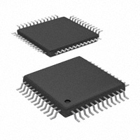


 工商网监
湘ICP备2023018690号
工商网监
湘ICP备2023018690号
