DAC7750, DAC8750
SBAS538D – DECEMBER 2013 – REVISED DECEMBER 2021
DACx750 Single-Channel, 12-Bit and 16-Bit Programmable Current Output
Digital-to-Analog Converters for 4-mA to 20-mA Current-Loop Applications
1 Features
3 Description
•
The DAC7750 and DAC8750 (DACx750) are lowcost, precision, fully-integrated, 12-bit and 16-bit
digital-to-analog converters (DACs) designed to
meet the requirements of industrial process-control
applications. These devices can be programmed as
a current output with ranges of 4 mA to 20 mA, 0 mA
to 20 mA, or 0 mA to 24 mA. The DACx750 include
reliability features such as CRC error checking on
the SPI frame, a watchdog timer, an open circuit,
compliance voltage, and thermal alarm. In addition,
the output current can be monitored by accessing an
internal precision resistor.
•
•
•
•
•
•
•
•
•
•
•
•
•
•
Current output options:
– 0 mA to 24 mA
– 4 mA to 20 mA
– 0 mA to 20 mA
±0.1% FSR typical total unadjusted error (TUE)
DNL: ±1 LSB maximum
Maximum loop compliance voltage: AVDD – 2 V
Internal 5-V reference: 10 ppm/°C (maximum)
Internal 4.6-V power-supply output
CRC frame error check
Watchdog timer
Thermal alarm
Open-circuit alarm
Pins to monitor output current
On-chip fault alarm
User-calibration for offset and gain
Wide temperature range: –40°C to +125°C
Packages: 6-mm × 6-mm 40-pin VQFN and 24-pin
HTSSOP
2 Applications
Analog output module
CPU (PLC controller)
Flow transmitter
Other sensor transmitter
Actuator
Process analytics (pH, gas, concentration, force
and humidity)
Device Information
DVDD
DVDD-EN
LATCH
SCLK
DIN
SDO
SPI Shift Register
Input Control Logic
DACx750
REFOUT
DACx750
REFIN
BODY SIZE (NOM)
HTSSOP (24)
7.80 mm × 4.40 mm
VQFN (40)
6.00 mm × 6.00 mm
For all available packages, see the orderable addendum at
the end of the data sheet.
AVDD
HART-IN
Internal
Reference
DAC Input
Register
R3-SENSE
Current Output Stage
Thermal
Alarm
BOOST
DAC
CLR
PACKAGE(1)
PART NUMBER
(1)
Control Logic
•
•
•
•
•
•
These devices include a power-on-reset function
designed to power up the device in a known state
(IOUT is disabled and in a Hi-Z state). The CLR pin
sets the current output to the low end of the range
if the output is enabled. Program the zero and gain
registers to digitally calibrate the device in the end
system. The output slew rate is also programmable by
register. These devices can superimpose an external
HART® signal on the current output, and operate with
a 10-V to 36-V supply.
PreConditioning
User Calibration
Gain/Offset
Register
IGAIN
IOUT
Current
Source
ALARM
IENABLE
ISET-R
Slew Rate
Control
Watchdog
Timer
GND
Block Diagram
An IMPORTANT NOTICE at the end of this data sheet addresses availability, warranty, changes, use in safety-critical applications,
intellectual property matters and other important disclaimers. PRODUCTION DATA.
�DAC7750, DAC8750
www.ti.com
SBAS538D – DECEMBER 2013 – REVISED DECEMBER 2021
Table of Contents
1 Features............................................................................1
2 Applications..................................................................... 1
3 Description.......................................................................1
4 Revision History.............................................................. 2
5 Device Comparison Table...............................................3
6 Pin Configuration and Functions...................................3
7 Specifications.................................................................. 5
7.1 Absolute Maximum Ratings........................................ 5
7.2 ESD Ratings............................................................... 5
7.3 Recommended Operating Conditions.........................5
7.4 Thermal Information....................................................6
7.5 Electrical Characteristics.............................................6
7.6 Electrical Characteristics: AC......................................9
7.7 Timing Requirements: Write Mode..............................9
7.8 Timing Requirements: Readback Mode......................9
7.9 Timing Diagrams ...................................................... 10
7.10 Typical Characteristics............................................ 11
8 Detailed Description......................................................19
8.1 Overview................................................................... 19
8.2 Functional Block Diagram......................................... 19
8.3 Feature Description...................................................20
8.4 Device Functional Modes..........................................27
8.5 Programming............................................................ 30
8.6 Register Maps...........................................................32
9 Application and Implementation.................................. 35
9.1 Application Information............................................. 35
9.2 Typical Application.................................................... 37
10 Power Supply Recommendations..............................40
11 Layout........................................................................... 40
11.1 Layout Guidelines................................................... 40
11.2 Layout Example...................................................... 41
12 Device and Documentation Support..........................42
12.1 Documentation Support.......................................... 42
12.2 Receiving Notification of Documentation Updates..42
12.3 Support Resources................................................. 42
12.4 Trademarks............................................................. 42
12.5 Electrostatic Discharge Caution..............................42
12.6 Glossary..................................................................42
13 Mechanical, Packaging, and Orderable
Information.................................................................... 42
4 Revision History
NOTE: Page numbers for previous revisions may differ from page numbers in the current version.
Changes from Revision C (January 2018) to Revision D (December 2021)
Page
• Updated the numbering format for tables, figures, and cross-references throughout the document..................1
• Changed Loop compliance voltage to Reference input voltage, and Reference input voltage to External
reference current in Recommended Operating Conditions ............................................................................... 5
• Changed Digital input low voltage test condition upper limit from 2.6 V to 3.6 V in Recommended Operating
Conditions ..........................................................................................................................................................5
• Deleted Timing Requirements: Daisy-Chain Mode section and Daisy-Chain Mode Timing figure................... 10
• Deleted Power-Supply Sequence section; content moved to Power Supply Recommendations section........ 21
• Deleted daisy-chain operation content from Watchdog Timer section..............................................................23
• Deleted The DACx750 Shares the SPI Bus With Other Devices subsection from Watchdog Timer section... 23
• Deleted daisy-chain operation from Frame Error Checking section................................................................. 23
• Added CRC fault reset command of 0x96 to Frame Error Checking section................................................... 23
• Deleted The DACx750 Shares the SPI Bus With Other Devices subsection................................................... 23
• Changed duplicated 010 step-size from 0.125 to 0.25 in Table 8-3, Slew Rate Step-Size Options ................ 25
• Added CRC fault reset command to Table 8-8, Write Address Functions ....................................................... 30
• Deleted Daisy-Chain Operation section............................................................................................................31
• Added Multiple Devices on the Bus section......................................................................................................31
• Changed Table 8-11 to delete daisy-chain operation and add CRC fault reset................................................ 32
• Changed DCEN to Reserved for DB3 in Control Register table.......................................................................32
• Deleted text stating CAP2 pin is only available for the 40-pin VQFN package.................................................35
• Added series resistance for supply and corrected HART-IN capacitance for Figure 9-3..................................37
• Added content from deleted Power-Supply Sequence section to Power Supply Recommendations section.. 40
• Added fast supply ramp and series resistance content to Power-Supply Recommendations ......................... 40
• Added power supply series resistance to Figure 11-1, Layout Example ......................................................... 41
Changes from Revision B (June 2016) to Revision C (January 2018)
Page
• Added last paragraph to User Calibration section............................................................................................ 24
• Added last paragraph to Programmable Slew Rate section............................................................................. 25
2
Submit Document Feedback
Copyright © 2021 Texas Instruments Incorporated
Product Folder Links: DAC7750 DAC8750
�DAC7750, DAC8750
www.ti.com
SBAS538D – DECEMBER 2013 – REVISED DECEMBER 2021
5 Device Comparison Table
PRODUCT
RESOLUTION
TUE (FSR)
DIFFERENTIAL
NONLINEARITY (LSB)
DAC8750
16
0.2%
±1
DAC7750
12
0.2%
±1
NC
DVDD
NC
GND
AVDD
NC
NC
NC
NC
NC
40
39
38
37
36
35
34
33
32
31
6 Pin Configuration and Functions
NC
1
30
NC
ALARM
2
29
CAP2
GND
3
28
CAP1
GND
4
27
BOOST
CLR
5
26
IOUT
ThermalPad
20
NC
NC
19
21
NC
10
NC
18
NC
REFIN
22
17
9
REFOUT
SDO
16
DVDD-EN
ISET-R
23
15
8
GND
DIN
14
HART-IN
13
24
GND
7
GND
SCLK
12
R3-SENSE
GND
25
11
6
NC
LATCH
Not to scale
Figure 6-1. RHA Package, 40-Pin VQFN, Top View
GND
1
24
AVDD
DVDD
2
23
NC
ALARM
3
22
CAP2
GND
4
21
CAP1
GND
5
20
BOOST
CLR
6
19
IOUT
ThermalPad
LATCH
7
18
R3-SENSE
SCLK
8
17
HART-IN
DIN
9
16
DVDD-EN
SDO
10
15
REFIN
GND
11
14
REFOUT
GND
12
13
ISET-R
Not to scale
Figure 6-2. PWP Package, 24-Pin HTSSOP, Top View
Submit Document Feedback
Copyright © 2021 Texas Instruments Incorporated
Product Folder Links: DAC7750 DAC8750
3
�DAC7750, DAC8750
www.ti.com
SBAS538D – DECEMBER 2013 – REVISED DECEMBER 2021
Table 6-1. Pin Functions
PIN
NAME
RHA
(VQFN)
PWP
(HTSSOP)
TYPE
DESCRIPTION
ALARM
2
3
Digital output
Alarm pin. Open drain output. External pullup resistor required (10 kΩ). The
pin goes low (active) when the ALARM condition is detected (open circuit,
over temperature, timeout, and so on).
AVDD
36
24
Supply input
Positive analog power supply.
BOOST
27
20
Analog output
Boost pin. External transistor connection (optional).
CAP1
28
21
Analog input
Connection for output filtering capacitor (optional).
CAP2
29
22
Analog input
Connection for output filtering capacitor (optional).
CLR
5
6
Digital input
Clear input. Logic high on this pin causes the part to enter CLEAR state.
Active high.
DIN
8
9
Digital input
Serial data input. Data are clocked into the 24-bit input shift register on the
rising edge of the serial clock input. Schmitt-Trigger logic input.
DVDD
39
2
Supply input
or output
Digital power supply. Can be input or output, depending on DVDD-EN pin.
23
16
Digital input
Internal power-supply enable pin. Connect this pin to GND to disable the
internal supply, or leave this pin unconnected to enable the internal supply.
When this pin is connected to GND, an external supply must be connected
to the DVDD pin.
GND
12, 13, 14,
15, 37
1, 11, 12
Supply input
Ground reference point for all analog circuitry of the device.
GND
3, 4
4, 5
Supply input
Ground reference point for all digital circuitry of the device.
HART-IN
24
17
Analog input
Input pin for HART modulation.
IOUT
26
19
Analog output
ISET-R
16
13
Analog input
Connection pin for external precision resistor (15 kΩ). See Section 8 of this
data sheet.
LATCH
6
7
Digital input
Load DAC registers input. A rising edge on this pin loads the input shift
register data into the DAC data and control registers and updates the DAC
output.
1, 10, 11,
19, 20, 21,
22, 30, 31,
32, 33, 34,
35, 38, 40
23
—
R3-SENSE
25
18
Analog output
This pin is used as a monitoring feature for the output current. The voltage
measured between the R3-SENSE pin and the BOOST pin is directly
proportional to the output current.
REFOUT
17
14
Analog output
Internal reference output. Connects to REFIN when using internal
reference.
REFIN
18
15
Analog input
Reference input
SCLK
7
8
Digital input
Serial clock input of the SPI. Data can be transferred at rates up to 30 MHz.
Schmitt-Trigger logic input.
SDO
9
10
Digital output
Serial data output. Data are valid on the rising edge of SCLK.
Supply input
The thermal pad is internally connected to GND. For enhanced thermal
performance, thermally connect the pad to a copper plane. The pad can
be electrically connected to the same potential as the GND pin or left
electrically unconnected provided a supply connection is made at the GND
pin.
DVDD-EN
NC
Thermal Pad
4
—
—
Current output pin
No connection.
Submit Document Feedback
Copyright © 2021 Texas Instruments Incorporated
Product Folder Links: DAC7750 DAC8750
�DAC7750, DAC8750
www.ti.com
SBAS538D – DECEMBER 2013 – REVISED DECEMBER 2021
7 Specifications
7.1 Absolute Maximum Ratings
over operating free-air temperature range (unless otherwise noted)(1)
MIN
MAX
AVDD to GND
–0.3
40
V
DVDD to GND
–0.3
6
V
IOUT to GND
–0.3
AVDD
V
REFIN to GND
–0.3
6
V
REFOUT to GND
–0.3
6
V
ALARM to GND
–0.3
6
V
Digital input voltage to GND
–0.3
DVDD + 0.3
V
SDO to GND
–0.3
DVDD + 0.3
Current into REFOUT
Operating temperature
TJ
Junction temperature
Tstg
Storage temperature
(1)
–40
–65
UNIT
V
10
mA
125
°C
150
°C
150
°C
Operation outside the Absolute Maximum Ratings may cause permanent device damage. Absolute Maximum Ratings do not imply
functional operation of the device at these or any other conditions beyond those listed under Recommended Operating Conditions.
If used outside the Recommended Operating Conditions but within the Absolute Maximum Ratings, the device may not be fully
functional, and this may affect device reliability, functionality, performance, and shorten the device lifetime.
7.2 ESD Ratings
VALUE
Electrostatic discharge(1)
VESD
(1)
(2)
(3)
Human body model (HBM) ESD stress
voltage(2)
±3000
Charged device model (CDM) ESD stress voltage(3)
±1000
UNIT
V
Electrostatic discharge (ESD) to measure device sensitivity and immunity to damage caused by assembly line electrostatic discharges
in to the device.
JEDEC document JEP155 states that 500-V HBM allows safe manufacturing with a standard ESD control process. Manufacturing with
less than 500-V HBM is possible with the necessary precautions.
JEDEC document JEP157 states that 250-V CDM allows safe manufacturing with a standard ESD control process. Manufacturing with
less than 250-V CDM is possible with the necessary precautions.
7.3 Recommended Operating Conditions
MIN
NOM
MAX
UNIT
AVDD
Analog supply voltage
10
36
V
DVDD
Digital supply voltage
2.7
5.5
V
Reference input voltage
4.95
External reference current
Loop compliance voltage (output = 24 mA)(1)
VIH
Digital input high voltage
VIL
Digital Input low voltage
AVDD – 2
V
V
3.6 V < AVDD < 5.5 V
0.8
2.7 V < AVDD < 3.6 V
0.6
–40
V
µA
2
Specified performance temperature
(1)
5.05
30
125
V
°C
Loop compliance voltage is defined as the voltage at the IOUT pin
Submit Document Feedback
Copyright © 2021 Texas Instruments Incorporated
Product Folder Links: DAC7750 DAC8750
5
�DAC7750, DAC8750
www.ti.com
SBAS538D – DECEMBER 2013 – REVISED DECEMBER 2021
7.4 Thermal Information
DAC7750, DAC8750
THERMAL
METRIC(1)
RHA (VQFN)
PWP (HTSSOP)
40 PINS
24 PINS
UNIT
RθJA
Junction-to-ambient thermal resistance
32.9
32.3
°C/W
RθJC(top)
Junction-to-case (top) thermal resistance
17.2
14.1
°C/W
RθJB
Junction-to-board thermal resistance
7.5
12.2
°C/W
ψJT
Junction-to-top characterization parameter
0.2
0.3
°C/W
ψJB
Junction-to-board characterization parameter
7.5
12
°C/W
RθJC(bot)
Junction-to-case (bottom) thermal resistance
1.4
0.63
°C/W
(1)
For more information about traditional and new thermal metrics, see the Semiconductor and IC Package Thermal Metrics application
report.
7.5 Electrical Characteristics
at AVDD = 10 V to 36 V, GND = 0 V, REFIN = 5 V external, DVDD = 2.7 V to 5.5 V, and all specifications are from –40°C to
+125°C (unless otherwise noted); for IOUT, RL = 300 Ω; typical specifications are at 25°C
PARAMETER
TEST CONDITIONS
MIN
TYP
MAX
UNIT
CURRENT OUTPUT
Current output
Resolution
RANGE bits = 111
0
24
RANGE bits = 110
0
20
RANGE bits = 101
4
20
DAC8750
16
DAC7750
12
mA
Bits
CURRENT OUTPUT ACCURACY (0 mA TO 20 mA AND 0 mA TO 24 mA)(1)
Total unadjusted error, TUE
Differential nonlinearity, DNL
Relative accuracy, INL(3)
Offset error
TA = –40°C to +125°C
–0.2%
0.2%
TA = –40°C to +85°C
–0.16%
0.16%
TA = 25°C
–0.08%
Monotonic
TA = –40°C to +125°C
±0.08%
TA = –40°C to +85°C
±0.024%
TA = –40°C to +125°C
–0.17%
TA = –40°C to +85°C
–0.1%
–0.07%
Offset error temperature coefficient
Full-scale error temperature coefficient
–0.2%
TA = –40°C to +85°C
–0.16%
TA = 25°C
–0.08%
Output current drift vs time
±5
6
ppm FSR/°C
ppm FSR/°C
–0.2%
0.2%
TA = –40°C to +85°C
–0.15%
0.15%
TA = 25°C
–0.08%
TA = –40°C to +125°C
–0.17%
0.17%
TA = –40°C to +85°C
–0.12%
0.12%
TA = 25°C
–0.05%
±0.01%
±0.01%
±3
External RSET
±8
Internal RSET
±50
External RSET
±25
Submit Document Feedback
FSR
0.08%
TA = –40°C to +125°C
Internal RSET
TA = 125°C, 1000 hrs
FSR
0.07%
0.16%
±0.015%
±10
External RSET
FSR
0.2%
External RSET
Gain error
Gain error temperature coefficient
0.1%
±0.01%
Internal RSET
Internal RSET
LSB
0.17%
±5
TA = –40°C to +125°C
FSR
0.08%
±1
TA = 25°C
Full-scale error
±0.02%
0.08%
FSR
0.05%
ppm FSR/°C
ppm FSR
Copyright © 2021 Texas Instruments Incorporated
Product Folder Links: DAC7750 DAC8750
�DAC7750, DAC8750
www.ti.com
SBAS538D – DECEMBER 2013 – REVISED DECEMBER 2021
7.5 Electrical Characteristics (continued)
at AVDD = 10 V to 36 V, GND = 0 V, REFIN = 5 V external, DVDD = 2.7 V to 5.5 V, and all specifications are from –40°C to
+125°C (unless otherwise noted); for IOUT, RL = 300 Ω; typical specifications are at 25°C
PARAMETER
TEST CONDITIONS
CURRENT OUTPUT ACCURACY (4 mA TO 20
Internal RSET
Total unadjusted error, TUE
External RSET
Relative accuracy, INL(3)
–0.25%
–0.08%
TA = –40°C to +125°C
–0.29%
0.29%
TA = –40°C to +85°C
–0.25%
0.25%
–0.1%
TA = –40°C to +85°C
±0.024%
External RSET
TA = –40°C to +125°C
–0.22%
0.22%
TA = –40°C to +85°C
–0.2%
0.2%
TA = –40°C to +125°C
–0.2%
0.2%
TA = –40°C to +85°C
–0.18%
0.18%
–0.07%
±0.01%
External RSET
–0.25%
TA = 25°C
–0 .08%
TA = –40°C to +125°C
–0.29%
0.29%
TA = –40°C to +85°C
–0.25%
0.25%
TA = 25°C
–0 .1%
±0.015%
±0.015%
External RSET
±10
External RSET
0.08%
ppm FSR/°C
–0.2%
0.2%
TA = –40°C to +85°C
–0.15%
0.15%
TA = 25°C
–0.08%
TA = –40°C to +125°C
–0.16%
0.16%
TA = –40°C to +85°C
–0.12%
0.12%
TA = 25°C
–0.05%
±0.01%
±0.01%
±3
External RSET
±8
Internal RSET
±50
External RSET
±75
FSR
0.1%
TA = –40°C to +125°C
Internal RSET
TA = 125°C, 1000 hrs
FSR
0.25%
±5
Gain error
FSR
ppm FSR/°C
TA = –40°C to +125°C
Internal RSET
Internal RSET
LSB
0.07%
±3
Full-scale error
FSR
0.1%
±1
Internal RSET
Output current drift vs time
±0.02%
0.08%
±0.08%
Internal and external RSET, TA = 25°C
Gain error temperature coefficient
UNIT
0.25%
±0.02%
TA = –40°C to +125°C
Offset error temperature coefficient
Full-scale error temperature coefficient
MAX
TA = 25°C
Monotonic
Internal RSET
Offset error
TYP
TA = –40°C to +125°C
TA = 25°C
Differential nonlinearity, DNL
MIN
mA)(1)
0.08%
FSR
0.05%
ppm FSR/°C
ppm FSR
CURRENT OUTPUT STAGE(2)
Loop compliance voltage(4)
Output = 24 mA
AVDD – 2
Inductive load(5)
50
DC PSRR
Output impedance
1
Code = 0x8000
V
mH
50
μA/V
MΩ
R3 RESISTOR
R3 resistor value
36
R3 resistor temperature coefficient
40
44
40
Ω
ppm/°C
EXTERNAL REFERENCE INPUT
Reference input voltage
External reference current
4.95
REFIN = 5.0 V
Reference input capacitance
5
5.05
V
30
μA
10
pF
Submit Document Feedback
Copyright © 2021 Texas Instruments Incorporated
Product Folder Links: DAC7750 DAC8750
7
�DAC7750, DAC8750
www.ti.com
SBAS538D – DECEMBER 2013 – REVISED DECEMBER 2021
7.5 Electrical Characteristics (continued)
at AVDD = 10 V to 36 V, GND = 0 V, REFIN = 5 V external, DVDD = 2.7 V to 5.5 V, and all specifications are from –40°C to
+125°C (unless otherwise noted); for IOUT, RL = 300 Ω; typical specifications are at 25°C
PARAMETER
TEST CONDITIONS
MIN
TYP
MAX
UNIT
INTERNAL REFERENCE OUTPUT
Reference output
TA = 25°C
Reference temperature coefficient(2)
TA = –40°C to +85°C
4.995
Output noise (0.1 Hz to 10 Hz)
TA = 25°C
Noise spectral density
TA = 25°C, 10 kHz
±10
Capacitive load
Load current
Short-circuit current
Load regulation
5.005
V
ppm/°C
14
μVPP
185
nV/√ Hz
600
nF
±5
mA
REFOUT shorted to GND
25
mA
AVDD = 24 V, TA = 25°C, sourcing
55
AVDD = 24 V, TA = 25°C, sinking
μV/mA
120
Line regulation
±1.2
μV/V
DVDD INTERNAL REGULATOR
Output voltage
AVDD = 24 V
4.6
Output load current(2)
Load regulation
3.5
Line regulation
Short-circuit current
V
10
mV/mA
1
AVDD = 24 V, to GND
mV/V
35
Capacitive load stability(2)
mA
mA
2.5
μF
DIGITAL INPUTS
High-level input voltage, VIH
Low-level input voltage, VIL
2
0.8
2.7 V < AVDD < 3.6 V
0.6
Hysteresis voltage
Input current
Pin capacitance
V
3.6 V < AVDD < 5.5 V
0.4
DVDD-EN, VIN ≤ 5 V
V
–2.7
All pins other than DVDD-EN
±1
Per pin
V
10
μA
pF
DIGITAL OUTPUTS
Low-level output voltage, VOL, sinking 200 μA
SDO
HIigh-level output voltage, VOH, sourcing 200 μA
0.4
DVDD – 0.5
High-impedance leakage
ALARM
Low-level output voltage,
VOL
±1
10-kΩ pullup resistor to
DVDD
0.4
2.5 mA
0.6
High-impedance leakage
±1
High-impedance output capacitance
10
V
μA
V
μA
pF
POWER SUPPLY
AVDD
DVDD
Internal regulator disabled
AIDD
10
36
V
2.7
5.5
V
Outputs disabled, external DVDD
3
Outputs disabled, internal DVDD
4
Code = 0x0000, IOUT enabled
3
DIDD
VIH = DVDD, VIL = GND, interface idle
Power dissipation
AVDD = 36 V, IOUT = 0 mA, DVDD = 5 V
95
mA
1
mA
115
mW
TEMPERATURE
Thermal alarm
Thermal alarm hysteresis
(1)
(2)
8
142
°C
18
°C
DAC8750 and DAC7750 current output range is set by writing to RANGE bits in control register at address 0x55.
Specified by design and characterization; not production tested.
Submit Document Feedback
Copyright © 2021 Texas Instruments Incorporated
Product Folder Links: DAC7750 DAC8750
�DAC7750, DAC8750
www.ti.com
(3)
(4)
(5)
SBAS538D – DECEMBER 2013 – REVISED DECEMBER 2021
For 0-mA to 20-mA and 0-mA to 24-mA ranges, INL is calculated beginning from code 0x0100 for DAC8750 and from code 0x0010 for
DAC7750.
Loop compliance voltage is defined as the voltage at the IOUT pin.
For stability, use slew rate limit feature or add a capacitor between IOUT and GND
7.6 Electrical Characteristics: AC
At AVDD = 10 V to 36 V, GND = 0 V, REFIN= 5 V external and DVDD = 2.7 V to 5.5 V. For IOUT, RL = 300 Ω. All
specifications –40°C to 125°C (unless otherwise noted). Typical specifications are at 25°C.
PARAMETER(1)
TEST CONDITIONS
MIN
TYP
MAX
UNIT
DYNAMIC PERFORMANCE
Output current settling time
10
μs
16-mA step, to 0.1% FSR, L < 1 mH
25
μs
–75
dB
200-mV, 50-Hz or 60-Hz sine wave superimposed
on power-supply voltage
AC PSRR
(1)
16-mA step, to 0.1% FSR, no L (inductance)
Specified by characterization, not production tested.
7.7 Timing Requirements: Write Mode
at TA = –40°C to 125°C and DVDD = 2.7 V to 5.5 V (unless otherwise noted)(1)
MIN
MAX
UNIT
t1
SCLK cycle time
33
ns
t2
SCLK low time
13
ns
t3
SCLK high time
13
ns
t4
LATCH delay time
13
ns
40
ns
5
ns
time(2)
t5
LATCH high
t6
Data setup time
t7
Data hold time
7
ns
t8
LATCH low time
40
ns
t9
CLR pulse duration
20
t10
CLR activation time
(1)
(2)
ns
5
µs
Specified by design, not production tested.
Based on digital interface circuitry only. When writing to DAC control and configuration registers, consider the analog output
specifications in Section 7.6.
7.8 Timing Requirements: Readback Mode
at TA = –40°C to 125°C and DVDD = 2.7 V to 5.5 V (unless otherwise noted)(1)
MIN
MAX
UNIT
t11
SCLK cycle time
60
ns
t12
SCLK low time
25
ns
t13
SCLK high time
25
ns
t14
LATCH delay time
13
ns
t15
LATCH high time
40
ns
t16
Data setup time
5
ns
t17
Data hold time
7
ns
t18
LATCH low time
40
ns
t19
Serial output delay time (CL, SDO = 15 pF)
35
ns
t20
LATCH rising edge to SDO 3-state (CL, SDO = 15 pF)
35
ns
(1)
Specified by design, not production tested.
Submit Document Feedback
Copyright © 2021 Texas Instruments Incorporated
Product Folder Links: DAC7750 DAC8750
9
�DAC7750, DAC8750
www.ti.com
SBAS538D – DECEMBER 2013 – REVISED DECEMBER 2021
7.9 Timing Diagrams
t1
1
SCLK
2
24
t3
t2
t4
t5
LATCH
t8
t7
t6
DB23
DIN
DB0
t9
CLR
t10
IOUT
Figure 7-1. Write Mode Timing
t11
t13
1
SCLK
2
24
2
8
9
22
23
24
t15
LATCH
t16
DIN
1
t14
t12
t18
t17
DB23
DB0
NOP condition
DB23
DB0
t20
Input word specifies
register to be read
t19
X
SDO
X
X
X
DB16
DB0
Undefined data
First eight bits are
don’t care bits
Selected register
data clocked out
Figure 7-2. Readback Mode Timing
10
Submit Document Feedback
Copyright © 2021 Texas Instruments Incorporated
Product Folder Links: DAC7750 DAC8750
�DAC7750, DAC8750
www.ti.com
SBAS538D – DECEMBER 2013 – REVISED DECEMBER 2021
7.10 Typical Characteristics
at TA = 25°C (unless otherwise noted)
25
5.004
5.003
20
5.002
Population (%)
Reference Output Voltage (V)
5.005
5.001
5.000
4.999
15
10
4.998
4.997
5
4.995
-40
-25
-10
5
20
35
50
65
80
95
110
Temperature (oC)
30 units shown
0
125
C003
0.0
1.0
1.0
1.5
2.0
2.5
3.0
3.5
4.0
4.5
5.0
5.5
6.0
6.5
7.0
7.5
8.0
8.5
9.0
9.5
10.0
4.996
Temperature Drift (ppm/oC)
AVDD = 24 V
C002
Figure 7-4. Internal Reference Temperature Drift Histogram
Figure 7-3. REFOUT vs Temperature
5.004
5.0050
5.003
5.0025
REFOUT (V)
REFOUT (V)
5.002
5.001
5.000
4.999
4.998
5.0000
4.9975
4.997
4.996
4.9950
-10
-8
-6
-4
-2
0
2
4
6
8
Load Current (mA)
10
10
14
18
22
26
30
34
AVDD (V)
C001
AVDD = 24 V
38
C002
TA = 25°C
Figure 7-5. REFOUT vs Load Current
Figure 7-6. REFOUT vs AVDD
1000
800
REFOUT Noise (2 µV/div)
VREF Noise PSD (nV/ rt-Hz)
900
700
600
500
400
300
200
100
0
10
100
1k
10k
Frequency (Hz)
Time (2 s/div)
100k
C006
AVDD = 24 V
C001
AVDD = 24 V
Figure 7-7. REFOUT Noise PSD vs Frequency
Figure 7-8. Internal Reference, Peak-to-Peak Noise
(0.1 Hz to 10 Hz)
Submit Document Feedback
Copyright © 2021 Texas Instruments Incorporated
Product Folder Links: DAC7750 DAC8750
11
�DAC7750, DAC8750
www.ti.com
SBAS538D – DECEMBER 2013 – REVISED DECEMBER 2021
7.10 Typical Characteristics (continued)
at TA = 25°C (unless otherwise noted)
3.0
2.5
AIDD (mA)
2.0
AVDD (4 V/div)
1.5
1.0
REFOUT (2 V/div)
0.5
0.0
Time (200 µs/div)
10
13
16
19
22
AVDD = 10 V
External DVDD
Figure 7-9. REFOUT Transient vs Time
28
31
34
37
C004
IOUT = 0 mA
Figure 7-10. AIDD vs AVDD
1.0
8
0.9
7
0.8
6
Internal DVDD (V)
0.7
DIDD (mA)
25
AVDD (V)
C002
0.6
0.5
0.4
0.3
5
4
3
2
0.2
1
0.1
0
-1
0.0
2.7
3.1
3.5
3.9
4.3
4.7
5.1
External DVDD (V)
TA = 25°C
-40
5.5
-35
-30
-25
-20
-15
-10
-5
0
Load Current (mA)
C001
TA = 25°C
External DVDD
5
C002
Internal DVDD
Figure 7-12. Internal DVDD vs Load Current
Figure 7-11. DIDD vs External DVDD
0
0.05
Total Unadjusted Error (%FSR)
Internal DVDD PSRR (dB)
-10
-20
-30
-40
-50
-60
-70
0.00
-0.05
-0.10
0 mA to 24 mA Internal RSET
-0.15
0 mA to 24 mA Internal RSET, BOOST
0 mA to 24 mA External RSET
-0.20
0 mA to 24 mA External RSET, BOOST
-80
-90
-0.25
10
100
1k
10k
100k
Frequency (Hz)
AVDD = 18 V
0
8192
16384
CLOAD = 100 nF
24576
32768
40960
49152
57344
Code
C001
AVDD = 24 V
Figure 7-13. Internal DVDD PSRR vs Frequency
12
1M
65536
C009
RLOAD = 300 Ω
Figure 7-14. IOUT TUE vs Code (0 mA to 24 mA)
Submit Document Feedback
Copyright © 2021 Texas Instruments Incorporated
Product Folder Links: DAC7750 DAC8750
�DAC7750, DAC8750
www.ti.com
SBAS538D – DECEMBER 2013 – REVISED DECEMBER 2021
7.10 Typical Characteristics (continued)
0.05
0.05
0.00
0.00
Total Unadjusted Error (%FSR)
Total Unadjusted Error (%FSR)
at TA = 25°C (unless otherwise noted)
-0.05
-0.10
0 mA to 20 mA Internal RSET
0 mA to 20 mA Internal RSET, BOOST
-0.15
0 mA to 20 mA External RSET
0 mA to 20 mA External RSET, BOOST
-0.20
-0.05
-0.10
-0.15
4 mA to 20 mA Internal RSET
4 mA to 20 mA Internal RSET, BOOST
-0.20
4 mA to 20 mA External RSET
4 mA to 20 mA External RSET, BOOST
-0.25
-0.25
0
8192
16384
24576
32768
40960
49152
57344
65536
Code
8192
16384
24576
32768
40960
49152
57344
RLOAD = 300 Ω
AVDD = 24 V
C003
RLOAD = 300 Ω
Figure 7-15. IOUT TUE vs Code (0 mA to 20 mA)
Figure 7-16. IOUT TUE vs Code (4 mA to 20 mA)
0.08
0.12
0.07
0.06
0.05
0.04
0.03
0 mA to 20 mA
0.02
0 mA to 24 mA
0.01
4 mA to 20 mA
65536
Code
C006
Total Unadjuated Error (%FSR)
Total Unadjusted Error (%FSR)
AVDD = 24 V
0
0.10
0.08
0.06
0.04
0 mA to 20 mA
0.02
0 mA to 24 mA
4 mA to 20 mA
0.00
0.00
-40
-25
-10
5
20
35
50
65
80
95
110
Temperature (oC)
AVDD = 10 V
-40
125
-10
5
20
35
50
65
80
95
110
125
Temperature (oC)
C008
RLOAD = 300 Ω
AVDD = 10 V
Figure 7-17. IOUT TUE vs Temperature (Internal RSET)
C009
RLOAD = 300 Ω
Figure 7-18. IOUT TUE vs Temperature (External RSET)
0.05
0.05
Max Total Unadjusted Error
0.04
Total Unadjusted Error (%FSR)
Total Unadjusted Error (%FSR)
-25
0.03
0.02
0.01
Min Total Unadjusted Error
0.00
Max Total Unadjusted Error
0.04
0.03
0.02
0.01
Min Total Unadjusted Error
-0.01
0
10
14
18
22
26
30
34
AVDD (V)
RLOAD = 300 Ω
38
10
14
0-mA to 24-mA range
Figure 7-19. IOUT TUE vs Supply (Internal RSET)
18
22
26
30
34
AVDD (V)
C006
RLOAD = 300 Ω
38
C005
0-mA to 24-mA range
Figure 7-20. IOUT TUE vs Supply (External RSET)
Submit Document Feedback
Copyright © 2021 Texas Instruments Incorporated
Product Folder Links: DAC7750 DAC8750
13
�DAC7750, DAC8750
www.ti.com
SBAS538D – DECEMBER 2013 – REVISED DECEMBER 2021
7.10 Typical Characteristics (continued)
at TA = 25°C (unless otherwise noted)
0.016
0.016
0 mA to 20 mA Internal RSET
0 mA to 24 mA Internal RSET
0.012
0.012
0 mA to 24 mA Internal RSET, BOOST
0 mA to 20 mA Internal RSET, BOOST
0 mA to 20 mA External RSET
0 mA to 24 mA External RSET
0.008
0 mA to 24 mA External RSET, BOOST
INL Error (%FSR)
INL Error (%FSR)
0.008
0.004
0.000
-0.004
-0.004
-0.008
-0.012
-0.012
-0.016
0
8192
16384
24576
32768
40960
49152
57344
65536
Code
AVDD = 24 V
0
8192
16384
24576
32768
40960
49152
57344
65536
Code
C007
RLOAD = 300 Ω
AVDD = 24 V
Figure 7-21. IOUT INL vs Code (0 mA to 24 mA)
C004
RLOAD = 300 Ω
Figure 7-22. IOUT INL vs Code (0 mA to 20 mA)
0.016
0.004
Max INL
4 mA to 20 mA Internal RSET
0.012
0.002
4 mA to 20 mA Internal RSET, BOOST
4 mA to 20 mA External RSET
0.008
4 mA to 20 mA External RSET, BOOST
INL Error (%FSR)
INL Error (%FSR)
0.000
-0.008
-0.016
0 mA to 20 mA External RSET, BOOST
0.004
0.004
0.000
-0.004
0.000
-0.002
-0.004
-0.008
-0.006
-0.012
Min INL
-0.016
-0.008
0
8192
16384
24576
32768
40960
49152
57344
Code
AVDD = 24 V
-40
65536
-10
5
20
35
50
65
80
95
110
Temperature (oC)
RLOAD = 300 Ω
AVDD = 10 V
Figure 7-23. IOUT INL vs Code (4 mA to 20 mA)
125
C002
RLOAD = 300 Ω
All IOUT ranges
Figure 7-24. IOUT INL vs Temperature (Internal RSET)
0.015
0.004
Max INL
Max INL
0.010
INL Error (%FSR)
0.002
INL Error (%FSR)
-25
C001
0.000
-0.002
-0.004
0.005
0.000
-0.005
Min INL
-0.006
-0.010
Min INL
-0.015
-0.008
-40
-25
-10
5
20
35
50
Temperature
AVDD = 10 V
65
80
95
110
125
(oC)
RLOAD = 300 Ω
All IOUT ranges
Figure 7-25. IOUT INL vs Temperature (External RSET)
14
10
14
18
22
26
30
34
AVDD (V)
C001
RLOAD = 300 Ω
38
C004
0-mA to 24-mA range
Figure 7-26. IOUT INL vs Supply (Internal RSET)
Submit Document Feedback
Copyright © 2021 Texas Instruments Incorporated
Product Folder Links: DAC7750 DAC8750
�DAC7750, DAC8750
www.ti.com
SBAS538D – DECEMBER 2013 – REVISED DECEMBER 2021
7.10 Typical Characteristics (continued)
at TA = 25°C (unless otherwise noted)
0.015
1.0
0.8
0.6
Max INL
0.005
DNL Error (LSB)
INL Error (% FSR)
0.010
0.000
-0.005
0.0
-0.2
-0.4
-0.8
Min INL
-0.015
-1.0
10
14
18
22
26
30
34
38
AVDD (V)
RLOAD = 300 Ω
0
8192
16384
24576
32768
40960
49152
57344
65536
Code
C003
0-mA to 24-mA range
AVDD = 24 V
RLOAD = 300 Ω
Figure 7-27. IOUT INL vs Supply (External RSET)
C008
0-mA to 24-mA range
Figure 7-28. IOUT DNL vs Code (0 mA to 24 mA)
1.0
1.0
0.8
0.8
0.6
0.6
0.4
0.4
DNL Error (LSB)
DNL Error (LSB)
0.2
-0.6
-0.010
0.2
0.0
-0.2
-0.4
0.2
0.0
-0.2
-0.4
-0.6
-0.6
-0.8
-0.8
-1.0
-1.0
0
8192
16384
24576
32768
40960
49152
57344
65536
Code
AVDD = 24 V
RLOAD = 300 Ω
0
8192
16384
24576
32768
40960
49152
57344
65536
Code
C005
0-mA to 24-mA range
AVDD = 24 V
RLOAD = 300 Ω
Figure 7-29. IOUT DNL vs Code (0 mA to 20 mA)
C002
4-mA to 24-mA range
Figure 7-30. IOUT DNL vs Code (4 mA to 20 mA)
1.0
1.0
0.8
0.8
Max DNL
0.6
0.6
0.4
0.4
DNL Error (LSB)
DNL Error (LSB)
0.4
0.2
0.0
-0.2
-0.4
-0.6
Max DNL
0.2
0.0
-0.2
-0.4
-0.6
-0.8
Min DNL
-0.8
Min DNL
-1.0
-1.0
-40
-25
-10
5
20
35
50
Temperature
AVDD = 10 V
65
80
95
110
125
(oC)
RLOAD = 300 Ω
-40
-25
-10
All IOUT ranges
Figure 7-31. IOUT DNL vs Temperature (Internal RSET)
5
20
35
50
65
80
95
110
125
Temperature (oC)
C010
AVDD = 10 V
RLOAD = 300 Ω
C011
All IOUT ranges
Figure 7-32. IOUT DNL vs Temperature (External RSET)
Submit Document Feedback
Copyright © 2021 Texas Instruments Incorporated
Product Folder Links: DAC7750 DAC8750
15
�DAC7750, DAC8750
www.ti.com
SBAS538D – DECEMBER 2013 – REVISED DECEMBER 2021
7.10 Typical Characteristics (continued)
at TA = 25°C (unless otherwise noted)
1.0
1.0
0.8
0.8
Max DNL
0.6
0.4
0.4
DNL Error (LSB)
DNL Error (LSB)
Max DNL
0.6
0.2
0.0
-0.2
-0.4
0.2
0.0
-0.2
-0.4
-0.6
-0.6
Min DNL
-0.8
-1.0
10
14
18
22
26
30
34
38
AVDD (V)
RLOAD = 300 Ω
10
14
18
22
26
30
34
38
AVDD (V)
C008
0-mA to 24-mA range
RLOAD = 300 Ω
C007
0-mA to 24-mA range
Figure 7-33. IOUT DNL vs Supply (Internal RSET)
Figure 7-34. IOUT DNL vs Supply (External RSET)
0.18
0.12
0.09
Offset Error (%FSR)
0.12
Full Scale Error (%FSR)
Min DNL
-0.8
-1.0
0.06
0.00
0 mA to 20 mA Internal RSET
-0.06
0 mA to 24 mA Internal RSET
0.06
0.03
0.00
0 mA to 20 mA Internal RSET
-0.03
0 mA to 24 mA Internal RSET
4 mA to 20 mA Internal RSET
-0.06
4 mA to 20 mA Internal RSET
0 mA to 20 mA External RSET
0 mA to 20 mA External RSET
-0.12
0 mA to 24 mA External RSET
-0.09
0 mA to 24 mA External RSET
4 mA to 20 mA External RSET
4 mA to 20 mA External RSET
-0.18
-0.12
-40
-25
-10
5
20
35
50
65
80
95
110
Temperature (oC)
AVDD = 10 V
125
-40
-25
-10
5
20
35
50
65
80
95
110
Temperature (oC)
C006
RLOAD = 300 Ω
AVDD = 10 V
Figure 7-35. IOUT Full-Scale Error vs Temperature
125
C003
RLOAD = 300 Ω
Figure 7-36. IOUT Offset Error vs Temperature
0.12
44
0 mA to 20 mA Internal RSET
0 mA to 24 mA Internal RSET
0.09
43
4 mA to 20 mA Internal RSET
0 mA to 20 mA External RSET
42
0 mA to 24 mA External RSET
4 mA to 20 mA External RSET
0.03
R3 (ohm)
Gain Error (%FSR)
0.06
0.00
40
-0.03
39
-0.06
38
-0.09
37
36
-0.12
-40
-25
-10
5
20
35
50
Temperature
AVDD = 10 V
65
80
95
110
(oC)
125
-40
-25
-10
5
20
35
50
65
80
95
Temperature (oC)
C007
110
125
C001
33 units shown
RLOAD = 300 Ω
Figure 7-37. IOUT Gain Error vs Temperature
16
41
Figure 7-38. R3 Resistance vs Temperature
Submit Document Feedback
Copyright © 2021 Texas Instruments Incorporated
Product Folder Links: DAC7750 DAC8750
�DAC7750, DAC8750
www.ti.com
SBAS538D – DECEMBER 2013 – REVISED DECEMBER 2021
7.10 Typical Characteristics (continued)
at TA = 25°C (unless otherwise noted)
2.00
Compliance Headroom Voltage (V)
30
Population (%)
25
20
15
10
5
1.75
1.50
1.25
1.00
0.75
0.50
0.25
-40
45
44
43
42
41
40
39
38
37
35
36
0.00
0
-25
-10
5
20
35
50
65
80
95
Temperature (oC)
R3 Temperature Drift (ppm/ oC)
C002
Figure 7-39. R3 Resistance Temperature Drift Histogram
110
125
C004
AVDD = 36 V
IOUT = 24 mA
RLOAD = 300 Ω
NOTE: Compliance voltage headroom is defined as the drop
from the AVDD pin to the IOUT pin.
Figure 7-40. Compliance Headroom Voltage vs Temperature
30
25
IOUT (mA)
20
IOUT (4 mA/div)
LATCH (5 V/div)
15
10
5
0
0
1
2
3
4
5
Headroom Voltage (V)
Time (5 µs/div)
6
C005
AVDD = 36 V
RLOAD = 300 Ω
DAC configured to deliver 24 mA
NOTE: Compliance voltage headroom is defined as the drop
from the AVDD pin to the IOUT pin.
C001
AVDD = 24 V
4-mA to 20-mA range
RLOAD = 300 Ω From code: 0x0000
To code: 0xFFFF
Figure 7-41. IOUT vs Compliance Headroom Voltage
Figure 7-42. 4-mA to 20-mA Rising
IOUT (4 mA/div)
IOUT (2 µA/div)
LATCH (5 V/div)
Time (60 µs/div)
Time (5 µs/div)
C001
C001
AVDD = 24 V
4-mA to 20-mA range
RLOAD = 300 Ω From code: 0x0000
To code: 0xFFFF
Figure 7-43. 4-mA to 20-mA Falling
AVDD = 24 V
RLOAD = 300 Ω
Figure 7-44. IOUT Power-On Glitch
Submit Document Feedback
Copyright © 2021 Texas Instruments Incorporated
Product Folder Links: DAC7750 DAC8750
17
�DAC7750, DAC8750
www.ti.com
SBAS538D – DECEMBER 2013 – REVISED DECEMBER 2021
7.10 Typical Characteristics (continued)
at TA = 25°C (unless otherwise noted)
1.0
8000h to 7FFFh
0.8
IOUT (200 µA/div)
7FFFh to 8000h
IOUT (mA)
0.6
0.4
0.2
0.0
-0.2
Time (2 µs/div)
Time (2 µs/div)
C001
C002
AVDD = 24 V
RLOAD = 300 Ω
AVDD = 24 V
Figure 7-45. IOUT Output Enable Glitch
RLOAD = 250 Ω
Figure 7-46. IOUT Digital-to-Analog Glitch
1000
IOUT Noise (20 nA/div)
IOUT Noise PSD (nV/ sqrt-Hz)
1200
800
600
400
200
0
10
100
1k
10k
AVDD = 24 V
RLOAD = 300 Ω
AVDD = 24 V
DAC = midscale
All IOUT ranges
0-mA to 20-mA range
Figure 7-48. IOUT Peak-to-Peak Noise vs Time (0.1 Hz to 10 Hz)
3.5
0
3.0
-10
-20
2.5
IOUT PSRR (dB)
Leakage Current (nA)
C002
C003
Figure 7-47. IOUT Noise PSD vs Frequency
2.0
1.5
1.0
0.5
-30
-40
-50
-60
-70
0.0
-80
-90
-0.5
0
4
8
12
16
20
24
28
32
IOUT Terminal Voltage (V)
AVDD = 36 V
36
10
100
1k
10k
100k
Frequency (Hz)
C001
AVDD = 24 V
Output disabled
Figure 7-49. IOUT Hi-Z Leakage Current vs Voltage
18
Time (4 s/div)
100k
Frequency (Hz)
RLOAD = 250 Ω
1M
C002
All IOUT ranges
Figure 7-50. IOUT PSRR vs Frequency
Submit Document Feedback
Copyright © 2021 Texas Instruments Incorporated
Product Folder Links: DAC7750 DAC8750
�DAC7750, DAC8750
www.ti.com
SBAS538D – DECEMBER 2013 – REVISED DECEMBER 2021
8 Detailed Description
8.1 Overview
The DAC8750 and DAC7750 are low-cost, precision, fully-integrated, 16-bit and 12-bit digital-to-analog
converters (DACs) designed to meet the requirements of industrial process control applications. These devices
can be programmed as a current output with a range of 4 mA to 20 mA, 0 mA to 20 mA, or 0 mA to 24 mA. The
DAC8750 and DAC7750 include reliability features such as CRC error checking on the serial peripheral interface
(SPI) frame, a watchdog timer, an open circuit, compliance voltage, and thermal alarm. In addition the output
current can be monitored by accessing an internal precision resistor.
These devices include a power-on-reset function to ensure powering up in a known state (both IOUT is disabled
and in a high-impedance state). The CLR pin sets the current output to the low-end of the range if the output is
enabled. Zero code error and gain error calibration registers can be programmed to digitally calibrate the device
in the end system. The output slew rate is also programmable. These devices can AC couple an external HART
signal on the current output and can operate with either a 10-V to 36-V supply.
8.2 Functional Block Diagram
DVDD
DVDD-EN
LATCH
SCLK
DIN
SDO
SPI Shift Register
Input Control Logic
DACx750
REFOUT
REFIN
Internal
Reference
DAC Input
Register
Control Logic
R3-SENSE
Current Output Stage
Thermal
Alarm
BOOST
DAC
CLR
AVDD
HART-IN
PreConditioning
User Calibration
Gain/Offset
Register
IGAIN
IOUT
Current
Source
ALARM
IENABLE
ISET-R
Slew Rate
Control
Watchdog
Timer
GND
Submit Document Feedback
Copyright © 2021 Texas Instruments Incorporated
Product Folder Links: DAC7750 DAC8750
19
�DAC7750, DAC8750
www.ti.com
SBAS538D – DECEMBER 2013 – REVISED DECEMBER 2021
8.3 Feature Description
8.3.1 DAC Architecture
The resistor-string section is simply a string of resistors, each with the same value, from REFIN to GND, as
Figure 8-1 shows. This type of architecture makes sure the DAC is monotonic. The 16-bit (DAC8750) or 12-bit
(DAC7750) binary digital code loaded to the DAC register determines at which node on the string the voltage
is tapped off before it is fed into the voltage-to-current conversion stage. The current-output stage converts the
voltage output from the string to current. When the output is disabled, it is in a high-impedance (Hi-Z) state. After
power-on, the output is disabled.
To Current Output
Figure 8-1. DAC Structure: Resistor String
8.3.2 Current Output Stage
The current output stage consists of a preconditioner and a current source, as shown in Figure 8-2. This stage
provides a current output according to the DAC code. The output range can be programmed as 0 mA to 20 mA,
0 mA to 24 mA, or 4 mA to 20 mA. Use an external transistor to reduce the power dissipation of the device. The
maximum compliance voltage on IOUT equals (AVDD – 2 V). In single power-supply mode, the maximum AVDD
is 36 V, and the maximum compliance voltage is 34 V. After power on, the IOUT pin is in a Hi-Z state.
AVDD
R3-SENSE
R2
R3
BOOST
T2
í
+
12-/16-BitBa_
DACBa_
A2
T1
+
IOUT
A1
í
RSET
Figure 8-2. Current Output
20
Submit Document Feedback
Copyright © 2021 Texas Instruments Incorporated
Product Folder Links: DAC7750 DAC8750
�DAC7750, DAC8750
www.ti.com
SBAS538D – DECEMBER 2013 – REVISED DECEMBER 2021
For a 5-V reference, the output can be expressed as shown in Equation 1 through Equation 3.
For a 0-mA to 20-mA output range, use Equation 1.
IOUT = 20mA •
CODE
2N
(1)
For a 0-mA to 24-mA output range, use Equation 2.
IOUT = 24mA •
CODE
2N
(2)
For a 4-mA to 20-mA output range, use Equation 3.
IOUT = 16mA •
CODE
2N
+ 4mA
(3)
where
•
•
CODE is the decimal equivalent of the code loaded to the DAC
N is the bits of resolution; 16 for DAC8750, and 12 for DAC7750
The current-output range is normally set according to the value of the RANGE bits in the Control Register (see
Section 8.4.1 for more details).
8.3.3 Internal Reference
The DACx750 includes an integrated 5-V reference with a buffered output (REFOUT) capable of driving up
to 5 mA (source or sink) with an initial accuracy of ±5 mV maximum and a temperature drift coefficient of 10
ppm/°C maximum.
8.3.4 Digital Power Supply
An internally generated 4.6-V supply capable of driving up to 10 mA can be output on DVDD by leaving the
DVDD-EN pin unconnected. This configuration simplifies the system power-supply design when an isolation
barrier is required to generate the digital supply. The internally generated supply can be used to drive isolation
components used for the digital data lines and other miscellaneous components, such as references and
temperature sensors; see Figure 9-3 for an example application.
If an external supply is preferred, the DVDD pin (which can be driven up to 5.5 V in this case) can become an
input by tying DVDD-EN to GND. See Section 7.5 for detailed specifications.
8.3.5 DAC Clear
The DAC has an asynchronous clear function through the CLR pin that is active-high and allows the current
output to be cleared to zero-scale code. When the CLR signal returns to low, the output remains at the cleared
value. The preclear value can be restored by pulsing the LATCH signal without clocking any data. A new value
cannot be programmed until the CLR pin returns to low. To avoid glitches on the output, disable the output by
writing a 0 to the OUTEN bit of the Control Register before changing the current range.
8.3.6 Power-On Reset
The DACx750 incorporates two internal POR circuits for the DVDD and AVDD supplies. The DVDD and AVDD
POR signals are ANDed together so that both supplies must be at their minimal specified values for the device
to not be in a reset condition. These POR circuits initialize internal logic and registers, as well as set the analog
outputs to a known state while the device supplies are ramping. All registers are reset to their default values.
Typically the POR function can be ignored, as long as the device supplies power-up and maintains the specified
minimum voltage levels. However, in the case of a supply drop or brownout, the DACx750 can have an internal
POR reset event or lose digital memory integrity. Figure 8-3 represents the threshold levels for the internal POR
for both the DVDD and AVDD supplies.
Submit Document Feedback
Copyright © 2021 Texas Instruments Incorporated
Product Folder Links: DAC7750 DAC8750
21
�DAC7750, DAC8750
www.ti.com
SBAS538D – DECEMBER 2013 – REVISED DECEMBER 2021
Supply (V)
Supply Max.
No Power-On Reset
Specified Supply
Voltage Range
Supply Min.
Undefined Operation Threshold
Undefined
POR Threshold
Power-On Reset
0.00
Figure 8-3. Relevant Voltage Levels for POR Circuit
For the DVDD supply, no internal POR occurs for nominal supply operation from 2.7 V (supply min) to 5.5 V
(supply max). For the DVDD supply region between 2.4 V (undefined operation threshold) and 0.8 V (POR
threshold), the internal POR circuit may or may not provide a reset over all temperature conditions. For the
DVDD supply below 0.8 V (POR threshold), the internal POR resets if the supply voltage remains less than 0.8 V
for approximately 1 ms.
For the AVDD supply, no internal POR occurs for nominal supply operation from 10 V (supply min) to 36 V
(supply max). For AVDD supply voltages between 8 V (undefined operation threshold) and 1 V (POR threshold),
the internal POR circuit may or may not provide a reset over all temperature conditions. For the AVDD supply
below 1 V (POR threshold), the internal POR resets if the supply voltage remains less than 1 V for approximately
1 ms. In case the DVDD or AVDD supply drops to a level where the internal POR signal is indeterminate, either
power cycle the device, or toggle the LATCH pin and then perform a software reset. Both options initialize the
internal circuitry to a known state and provide proper operation.
8.3.7 Alarm Detection
These devices also provide an alarm detection feature. When one or more of following events occur, the ALARM
pin goes low:
•
•
•
•
•
The current output load is in open circuit,
The voltage at IOUT reaches a level where accuracy of the output current is compromised. This condition
is detected by monitoring internal voltage levels of the IOUT circuitry and is typically below the specified
compliance voltage headroom (defined as the voltage drop between the AVDD and IOUT pins) minimum of 2
V,
The die temperature exceeds 142°C,
The SPI watchdog timer exceeds the timeout period (if enabled), or
The SPI frame error CRC check encounters an error (if enabled).
When the ALARM pins of multiple DACx750 devices are connected together to form a wired-AND function, the
host processor must read the status register of each device to know all the fault conditions that are present. Note
that the thermal alarm has hysteresis of approximately 18°C. After being set, the alarm only resets when the die
temperature drops below 124°C.
22
Submit Document Feedback
Copyright © 2021 Texas Instruments Incorporated
Product Folder Links: DAC7750 DAC8750
�DAC7750, DAC8750
www.ti.com
SBAS538D – DECEMBER 2013 – REVISED DECEMBER 2021
8.3.8 Watchdog Timer
This feature is useful to make sure that communication between the host processor and the DACx750 has not
been lost. The feature can be enabled by setting the WDEN bit of the Configuration Register to 1. The watchdog
timeout period can be set using the WDPD bits of the configuration register, as shown in Table 8-1. The timer
period is based off an internal oscillator with a typical value of 8 MHz.
Table 8-1. Watchdog Timeout Period
WDPD BITS
WATCHDOG TIMEOUT PERIOD (Typical)
00
10 ms
01
51 ms
10
102 ms
11
204 ms
If the watchdog timer is enabled, these devices must have an SPI frame with 0x95 as the write address byte
written to the device within the programmed timeout period. Otherwise, the ALARM pin asserts low and the
WD-FLT bit of the status register is set to 1. The ALARM pin can be asserted low for any of the different
conditions explained in Section 8.3.7. To reset the WD-FLT bit to 0, use a software reset, disable the watchdog
timer, or power down the device.
8.3.9 Frame Error Checking
In noisy environments, error checking can be used to check the integrity of SPI data communication between
the DACx750 and the host processor. To enable this feature, set the CRCEN bit of the Configuration Register
to 1. The frame error checking scheme is based on the CRC-8-ATM (HEC) polynomial x8 + x2 + x + 1 (that is,
100000111). When error checking is enabled, the SPI frame width is 32 bits, as shown in Table 8-2. Start with
the default 24-bit frame, enable frame error checking, and then switch to the 32-bit frame. The normal 24-bit
SPI data are appended with an 8-bit CRC polynomial by the host processor before feeding to the device. For a
register readback, the CRC polynomial is output on the SDO pins by the device as part of the 32-bit frame.
Table 8-2. SPI Frame with Frame Error Checking
Enabled
BIT 31:BIT 8
BIT 7:BIT 0
Normal SPI frame data
8-bit CRC polynomial
When in CRC mode, the DACx750 calculates CRC words every 32 clocks, unconditional of when the LATCH
pin toggles. The DACx750 decodes the 32-bit input frame data to compute the CRC remainder. If no error
exists in the frame, the CRC remainder is zero. When the remainder is non-zero (that is, the input frame has
single- or multiple-bit errors), the ALARM pin asserts low and the CRC-FLT bit of the status register is set to
1. The ALARM pin can be asserted low for any of the different conditions explained in Section 8.3.7. To reset
the CRC-FLT bit to 0, either issue software reset command of 0x96, disable the frame error checking, or power
down the device. In the case of a CRC error, the specific SPI frame is blocked from writing to the device.
If CRC mode is enabled on the first frame issued to the device after power up, issue a no operation, or NOOP,
command to the device in order to reset the SPI clock and SPI frame alignment in the event that any transients
on the SCLK line are interpreted as SCLK periods. A NOOP command can be issued to the device by simply
toggling the LATCH pin without any SCLK periods.
Submit Document Feedback
Copyright © 2021 Texas Instruments Incorporated
Product Folder Links: DAC7750 DAC8750
23
�DAC7750, DAC8750
www.ti.com
SBAS538D – DECEMBER 2013 – REVISED DECEMBER 2021
8.3.10 User Calibration
The device implements a user-calibration function (enabled by the CALEN bit in the Configuration Register) to
trim system gain and zero errors. The DAC output is calibrated according to the value of the gain calibration and
zero calibration registers. The range of gain adjustment is typically ±50% of full-scale with 1 LSB per step. The
gain register must be programmed to 0x8000 to achieve the default gain of 1 because the power-on value of the
register is 0x0000, equivalent to a gain of 0.5. The zero code adjustment is typically ±32,768 LSBs with 1 LSB
per step. The input data format of the gain register is unsigned straight binary, and the input data format of the
zero register is 2's complement. The gain and offset calibration is described by Equation 4.
CODE _ OUT = CODE •
User _ GAIN + 215
216
+ User _ ZERO
(4)
where
•
•
•
•
•
CODE is the decimal equivalent of the code loaded to the DAC data register at address 0x01
N is the bits of resolution (16 for DAC8750 and 12 for DAC7750)
User_ZERO is the signed 16-bit code in the zero register
User_GAIN is the unsigned 16-bit code in the gain register
CODE_OUT is the decimal equivalent of the code loaded to the DAC (limited between 0x0000 to 0xFFFF for
DAC8750 and 0x000 to 0xFFF for DAC7750)
This is a purely digital implementation and the output is still limited by the programmed value at both ends of
the current output range (set by the RANGE bits, as described in Section 8.4.1). In addition, the correction only
makes sense for endpoints inside of the true device end points. To correct more than just the actual device error
(for example, a system offset), the valid range for the adjustment changes accordingly and must be taken into
account.
New calibration codes are only applied to subsequent writes to the DAC data register. Updating the calibration
codes does not automatically update the DAC output. Additionally, before applying new DAC data, configure the
calibration codes along with the slew rate control.
24
Submit Document Feedback
Copyright © 2021 Texas Instruments Incorporated
Product Folder Links: DAC7750 DAC8750
�DAC7750, DAC8750
www.ti.com
SBAS538D – DECEMBER 2013 – REVISED DECEMBER 2021
8.3.11 Programmable Slew Rate
The slew rate control feature controls the rate at which the output current changes. With the slew rate control
feature disabled, the output changes smoothly at a rate limited by the output drive circuitry and the attached
load.
To reduce the slew rate, enable the slew rate control feature through bit 4 of the Control Register. With this
feature enabled, the output does not slew directly between the two values. Instead, the output steps digitally at
a rate defined by bits [7:5] (SRSTEP) and bits [11:8] (SRCLK) of the Control Register. SRCLK defines the rate
at which the digital slew updates, and SRSTEP defines the amount by which the output value changes at each
update. If the DAC data register is read while the DAC output is still changing, the instantaneous value is read.
Table 8-3 lists the slew rate step-size options. Table 8-4 summarizes the slew rate update clock options.
Table 8-3. Slew Rate Step-Size (SRSTEP) Options
STEP SIZE (LSB)
SRSTEP
DAC7750
DAC8750
000
0.0625
1
001
0.125
2
010
0.25
4
011
0.5
8
100
1
16
101
2
32
110
4
64
111
8
128
Table 8-4. Slew Rate Update Clock (SRCLK) Options
SRCLK
DAC UPDATE FREQUENCY (Hz)
0000
258,065
0001
200,000
0010
153,845
0011
131,145
0100
115,940
0101
69,565
0110
37,560
0111
25,805
1000
20,150
1001
16,030
1010
10,295
1011
8,280
1100
6,900
1101
5,530
1110
4,240
1111
3,300
Submit Document Feedback
Copyright © 2021 Texas Instruments Incorporated
Product Folder Links: DAC7750 DAC8750
25
�DAC7750, DAC8750
www.ti.com
SBAS538D – DECEMBER 2013 – REVISED DECEMBER 2021
The time required for the output to slew over a given range is expressed as Equation 5.
Slew Time =
Output Change
Step Size · Update Clock Frequency · LSB Size
(5)
where
•
•
Slew Time is expressed in seconds
Output Change is expressed in amps (A) for IOUT or volts (V) for VOUT
When the slew rate control feature is enabled, all output changes happen at the programmed slew rate. This
configuration results in a staircase formation at the output. If the CLR pin is asserted, the output slews to the
zero-scale value at the programmed slew rate. Read bit 1 (SR-ON) of the Status Register to verify that the slew
operation has completed. The update clock frequency for any given value is the same for all output ranges. The
step size, however, varies across output ranges for a given value of step size because the LSB size is different
for each output range. Figure 8-4 shows an example of IOUT slewing at a rate set by the previously described
parameters. In this example for the DAC8750 (LSB size of 305 nA for the 0-mA to 20-mA range), the settings
correspond to an update clock frequency of 6.9 kHz and a step size of 128 LSB. As shown in the case with no
capacitors on CAP1 or CAP2, the steps occur at the update clock frequency (6.9 kHz corresponds to a period
close to 150 µs), and the size of each step is approximately 38 µA (128 × 305 nA). Calculate the slew time for a
specific code change by using Equation 5.
IOUT (38 µA/div)
no cap
3 nF CAP1
3 nF CAP2
10 nF CAP1
10 nF CAP2
SRCLK=1100h
SRSTEP = 111h
0 mA to 20 mA range
Time (150 µs/ div)
C001
Figure 8-4. IOUT vs Time With Digital Slew Rate Control
Apply the desired programmable slew rate control setting before updating the DAC data register because
updates to the DAC data register in tandem with updates to the slew rate control registers can create race
conditions that may result in unexpected DAC data.
26
Submit Document Feedback
Copyright © 2021 Texas Instruments Incorporated
Product Folder Links: DAC7750 DAC8750
�DAC7750, DAC8750
www.ti.com
SBAS538D – DECEMBER 2013 – REVISED DECEMBER 2021
8.4 Device Functional Modes
8.4.1 Setting Current-Output Ranges
The current output range is set according to Table 8-5.
Table 8-5. RANGE Bits vs Output Range
RANGE
OUTPUT RANGE
101
4 mA to 20 mA
110
0 mA to 20 mA
111
0 mA to 24 mA
Note that changing the RANGE bits at any time causes the DAC data register to be cleared.
8.4.2 Current-Setting Resistor
Resistor RSET (used to convert the DAC voltage to current) illustrated in Figure 8-2 determines the stability of the
output current over temperature. If desired, an external, low-drift, precision 15-kΩ resistor can be connected to
the ISET-R pin and used instead of the internal RSET resistor.
8.4.3 BOOST Configuration for IOUT
Figure 8-5 illustrates an external NPN transistor used to reduce power dissipation on the die. Most of the load
current flows through the NPN transistor with a small amount flowing through the on-chip PMOS transistor based
on the gain of the NPN transistor. This configuration reduces the temperature induced drift on the die and
internal reference and is an option for use cases at the extreme end of the supply, load current, and ambient
temperature ranges.
The inclusion of the bipolar junction transistor (BJT) adds an additional open loop gain to internal amplifier A2
(see Figure 8-2) and thus, can cause possible instability. Adding series emitter resistor R2 decreases the gain
of the stage created by the BJT and internal R3 resistor (see Figure 8-2) especially for cases where RLOAD is
a short or a very small load, such as a multimeter. Recommended values for R1, R2, and C1 in this circuit are
1 kΩ, 30 Ω and 22 nF, respectively. An equivalent solution is to place R2 (with a recommended value of 3 kΩ
instead of 30 Ω) in series with the base of the transistor instead of the configuration provided in Figure 8-5. Note
that there is some gain error introduced by this configuration; see Figure 7-14, Figure 7-15 and Figure 7-16. Use
the internal transistor in most cases because the values in Section 7.5 are based on the configuration with the
internal on-chip PMOS transistor.
BOOST
IOUT
R2
DACx750
R1
C1
RLOAD
GND
Copyright © 2016, Texas Instruments Incorporated
Figure 8-5. Boost Mode Configuration
Submit Document Feedback
Copyright © 2021 Texas Instruments Incorporated
Product Folder Links: DAC7750 DAC8750
27
�DAC7750, DAC8750
www.ti.com
SBAS538D – DECEMBER 2013 – REVISED DECEMBER 2021
8.4.4 Filtering The Current Output
The DACx750 provides access to internal nodes of the circuit; see Figure 9-2. Place capacitors on these pins
and AVDD to form a filter on the output current, reducing bandwidth and the slew rate of the output, especially
useful for driving inductive loads. However, to achieve large reductions in slew rate, use the programmable slew
rate to avoid having to use large capacitors. Even in that case, use the capacitors on CAP1 and CAP2 to smooth
out the stairsteps caused by the digital code changes as shown in Figure 8-6. However, note that power supply
ripple also couples into the devices through these capacitors.
25
22
IOUT (mA)
19
no cap
3 nF CAP1
3 nF CAP2
10 nF CAP1
10 nF CAP2
16
13
10
7
4
1
TA = 25ºC
AVDD = 24 V
RLOAD = 250 Ÿ
Time (200 µs/div)
C001
Figure 8-6. IOUT vs Time for Different Cap Values on CAP1 and CAP2
8.4.5 Output Current Monitoring
Many applications, especially for functional safety, require monitoring to make sure that the output current
stays close to the programmed value. To monitor the output current, place a sense resistor in series with the
output and measure the voltage across the resistor. However, this resistor reduces the compliance voltage
available for the load. The DACx750 provide access to an internal precision resistor (R3 in Figure 8-2) through
the R3-SENSE and BOOST pins to perform analog readback for monitoring the output current. Measure the
voltage between the R3-SENSE and BOOST pins and divide by the value of the R3 resistor to determine the
magnitude of the output current. The R3 resistor has a typical value of 40 Ω (see Figure 7-38 for a plot of
resistance vs temperature) with a temperature drift coefficient of 40 ppm/°C (see Figure 7-39 for a histogram of
R3 resistance temperature drift). The R3 resistor is tested to stay within the minimum (36 Ω) and maximum (44
Ω) resistance values shown in the R3 Resistor portion of Section 7.5. To remove the tolerance error, perform a
simple calibration by programming a certain value of output current, measuring the voltage across R3-SENSE
and BOOST, and calculating the exact value of R3.
28
Submit Document Feedback
Copyright © 2021 Texas Instruments Incorporated
Product Folder Links: DAC7750 DAC8750
�DAC7750, DAC8750
www.ti.com
SBAS538D – DECEMBER 2013 – REVISED DECEMBER 2021
8.4.6 HART Interface
For the DACx750, HART digital communication can be modulated onto the input signal by the methods shown in
the following subsections. For more detail, see Implementing HART Communication with the DAC8760 Family.
8.4.6.1 Implementing HART in 4-mA to 20-mA Mode
This method is limited to the case where the RANGE bits of the Control Register are programmed to the 4-mA
to 20-mA range. Some applications require going beyond the 4-mA to 20-mA range. In those cases, see the
methods described in the next subsection.
The external HART signal (ac voltage; 500 mVPP, 1200 Hz, and 2200 Hz) can be capacitively coupled in through
the HART-IN pin and transferred to a current that is superimposed on the 4-mA to 20-mA current output. The
HART-IN pin has a typical input impedance of 35 kΩ that together with the input capacitor used to couple the
external HART signal, forms a filter to attenuate frequencies beyond the HART band-pass region. In addition
to this filter, an external passive filter is recommended to complete the filtering requirements of the HART
specifications. Figure 8-7 shows the output current versus time operation for a typical HART signal. Table 8-6
specifies the performance of the HART-IN pin.
1200 Hz
(mark)
Phase
Continuous
2200 Hz
(space)
Bit
Boundary
Loop Current
6.5 mA
6.0 mA
5.5 mA
Bit Cell Time = 833 ms
Time
DC current = 6 mA.
Figure 8-7. Output Current vs Time
Table 8-6. HART-IN Pin Characteristics
PARAMETER
TEST CONDITIONS
Input impedance
HART signal ac-coupled into pin
Output current (peak-to-peak)
Input signal of 500 mV (peak-to-peak)
MIN
TYP
MAX UNIT
35
0.9
1
kΩ
1.1
mA
8.4.6.2 Implementing HART in All Current Output Modes
The use of the HART-IN pin to implement HART modulation is limited to the case where the RANGE bits of the
Section 8.6.1.1 are set to the 4-mA to 20-mA range. If it is desirable to implement HART in all current-output
modes, see Section 9.1.1.
Submit Document Feedback
Copyright © 2021 Texas Instruments Incorporated
Product Folder Links: DAC7750 DAC8750
29
�DAC7750, DAC8750
www.ti.com
SBAS538D – DECEMBER 2013 – REVISED DECEMBER 2021
8.5 Programming
Table 8-11 describes the available commands and registers on the DACx750 devices. No operation, read
operation, and watchdog timer refer to commands and are not explicit registers. For more information on these
commands, see Section 8.5.1.3 and Section 8.3.8.
8.5.1 Serial Peripheral Interface (SPI)
The device is controlled over a versatile four-wire serial interface (SDI, SDO, SCLK, and LATCH) that operates
at clock rates of up to 30 MHz and is compatible with SPI, QSPI, Microwire, and digital signal processing (DSP)
standards. The SPI communication command consists of a write address byte and a data word for a total of 24
bits. The timing for the digital interface is illustrated in Figure 7-1 and Figure 7-2.
8.5.1.1 SPI Shift Register
The default frame is 24 bits wide (see Section 8.3.9 for 32-bit frame mode) and begins with the rising edge of
SCLK that clocks in the MSB. The subsequent bits are latched on successive rising edges of SCLK. The default
24-bit input frame consists of an 8-bit address byte followed by a 16-bit data word as shown in Table 8-7.
Table 8-7. Default SPI Frame
BIT 23:BIT 16
BIT 15:BIT 0
Address byte
Data word
The host processor must issue 24 bits before it issues a rising edge on the LATCH pin. Input data bits are
clocked in regardless of the LATCH pin and are unconditionally latched on the rising edge of LATCH. By default,
the SPI shift register resets to 0x000000 at power on or after a reset.
8.5.1.2 Write Operation
A write operation is accomplished when the address byte is set according to Table 8-8. For more information on
the DACx750 registers, see Section 8.6.
Table 8-8. Write Address Functions
ADDRESS
BYTE
(HEX)
30
FUNCTION
00
No operation (NOP)
01
Write DAC Data register
02
Register read
55
Write control register
56
Write reset register
57
Write configuration register
58
Write DAC gain calibration register
59
Write DAC zero calibration register
95
Watchdog timer reset
96
CRC error reset
Submit Document Feedback
Copyright © 2021 Texas Instruments Incorporated
Product Folder Links: DAC7750 DAC8750
�DAC7750, DAC8750
www.ti.com
SBAS538D – DECEMBER 2013 – REVISED DECEMBER 2021
8.5.1.3 Read Operation
A read operation is accomplished when the address byte is 0x02. Follow the read operation with a no-operation
(NOP) command to clock out an addressed register; see Figure 7-2. To read from a register, the address byte
and data word is as shown in Table 8-9. The read register value is output MSB first on SDO on successive falling
edges of SCLK.
Table 8-9. Default SPI Frame for Register Read
DATA WORD
ADDRESS BYTE
(HEX)
BIT 15:BIT 6
BIT 5:BIT 0
02
X (don't care)
Register read address (see Table 8-10)
Table 8-10 shows the register read addresses available on the DACx750 devices.
Table 8-10. Register Read Address Functions
READ
(1)
ADDRESS(1)
FUNCTION
XX XX00
Read status register
XX XX01
Read DAC data register
XX XX10
Read control register
00 1011
Read configuration register
01 0011
Read DAC gain calibration register
01 0111
Read DAC zero calibration register
X denotes don't care bits.
8.5.1.4 Stand-Alone Operation
SCLK can operate in either continuous or burst mode, as long as the LATCH rising edge occurs after the
appropriate number of SCLK cycles. Providing more than or less than 24 SCLK cycles before the rising edge of
LATCH results in incorrect data being programmed into the device registers, and incorrect data sent out on SDO.
The rising edge of SCLK that clocks in the MSB of the 24-bit input frame marks the beginning of the write cycle,
and data are written to the addressed registers on the rising edge of LATCH.
8.5.1.5 Multiple Devices on the Bus
Communication with the device is not directly gated by LATCH; therefore, do not connect multiple devices in
parallel without gating SCLK. Figure 8-8 shows two devices with SCLK gated for each device.
CS1
LATCH1
SCLK
SCLK
SDO
DIN
DIN
DOUT
Device 1
CS2
Microcontroller
LATCH2
SCLK
SDO
DIN
Device 2
Figure 8-8. Multiple Devices on the Bus Using Gated SCLK
The microcontroller uses two chip select lines, one for each LATCH pin. Each line is used to gate the SCLK for
communication for each device.
Submit Document Feedback
Copyright © 2021 Texas Instruments Incorporated
Product Folder Links: DAC7750 DAC8750
31
�DAC7750, DAC8750
www.ti.com
SBAS538D – DECEMBER 2013 – REVISED DECEMBER 2021
8.6 Register Maps
Table 8-11 shows the available registers on the DACx750 devices. See Section 8.6.1 for descriptions of all
DACx750 registers.
Table 8-11. Command and Register Map
READ AND
WRITE
ACCESS
15:14
13
12
Control
RW
X
REXT
OUTEN
Configuration
RW
REGISTER OR
COMMAND
DAC
Data(2)
11
10:9
8
—
Read Operation (3)
—
Reset
W
Status
R
7
6
SRCLK
5
SRSTEP
X(1)
RW
No operation(3)
DAC Gain Calibration
DATA BITS (DB15:DB0)
CALEN
0
WDEN
WDPD
RESET
Reserved
CRC-FLT
Watchdog Timer
Reset (3)
—
X
CRC Fault Reset (3)
—
X
(3)
1
RANGE
READ ADDRESS
Z15:Z0, signed
(1)
(2)
CRCEN
2
X
RW
(2)
HARTEN
X
G15:G0, unsigned
DAC Zero Calibration
3
Reserved
D15:D0
RW
(2)
4
SREN
WD-FLT
I-FLT
SR-ON
T-FLT
X denotes don't care bits.
DAC8750 (16-bit version) shown. DAC7750 (12-bit version) contents are located in DB15:DB4.
For DAC7750, DB3:DB0 are don't care bits when writing and zeros when reading.
No operation, read operation, watchdog timer reset, and CRC fault reset are commands and not registers.
8.6.1 DACx750 Register Descriptions
8.6.1.1 Control Register
The DACx750 control register is written to at address 0x55. Table 8-12 shows the description for the control
register bits.
Table 8-12. Control Register
32
DATA BIT(S)
NAME
DEFAULT
DESCRIPTION
DB15:DB14
Reserved
00
Reserved. Do not write any value other than zero to these bits.
DB13
REXT
0
External current setting resistor enable.
DB12
OUTEN
0
Output enable.
Bit = 1: Output is determined by RANGE bits.
Bit = 0: Output is disabled. IOUT is Hi-Z.
DB11:DB8
SRCLK[3:0]
0000
Slew rate clock control. Ignored when bit SREN = 0.
DB7:DB5
SRSTEP[2:0]
000
Slew rate step size control. Ignored when bit SREN = 0.
DB4
SREN
0
Slew Rate Enable.
Bit = 1: Slew rate control is enabled, and the ramp speed of the output change is determined
by SRCLK and SRSTEP.
Bit = 0: Slew rate control is disabled. Bits SRCLK and SRSTEP are ignored. The output
changes to the new level immediately.
DB3
Reserved
0
Reserved. Must be set to 0.
DB2:DB0
RANGE[2:0]
000
Output range bits.
Submit Document Feedback
Copyright © 2021 Texas Instruments Incorporated
Product Folder Links: DAC7750 DAC8750
�DAC7750, DAC8750
www.ti.com
SBAS538D – DECEMBER 2013 – REVISED DECEMBER 2021
8.6.1.2 Configuration Register
The DACx750 configuration register is written to at address 0x57. Table 8-13 summarizes the description for the
configuration register bits.
Table 8-13. Configuration Register
DATA BIT(S)
NAME
DEFAULT
DB15:DB6
Reserved
00 0000 0000
DESCRIPTION
DB5
CALEN
0
User calibration enable. When user calibration is enabled, the DAC data are
adjusted according to the contents of the gain and zero calibration registers. See
the Section 8.3.10 section.
Reserved. Do not write any value other than zero to these bits.
DB4
HARTEN
0
Enable interface through HART-IN pin (only valid for IOUT set to 4-mA to 20-mA
range through RANGE bits).
Bit = 1: HART signal is connected through internal resistor and modulates output
current.
Bit = 0: HART interface is disabled.
DB3
CRCEN
0
Enable frame error checking.
DB2
WDEN
0
Watchdog timer enable.
DB1:DB0
WDPD[1:0]
00
Watchdog timeout period.
8.6.1.3 DAC Registers
The DAC registers consist of a DAC data register (Table 8-14), a DAC gain calibration register (Table 8-15),
and a DAC zero calibration register (Table 8-16). User calibration as described in Section 8.3.10 is a feature
that allows for trimming the system gain and zero errors. Table 8-14 through Table 8-16 show the DAC8750,
16-bit version of these registers. The DAC7750 (12-bit version) register contents are located in DB15:DB4. For
DAC7750, DB3:DB0 are don't care bits when writing and zeros when reading.
Table 8-14. DAC Data Register
DATA BITS
NAME
DEFAULT
DB15:DB0
D15:D0
0x0000
DATA BITS
NAME
DEFAULT
DB15:DB0
G15:G0
0x0000
DATA BITS
NAME
DEFAULT
DB15:DB0
Z15:Z0
0x0000
DESCRIPTION
DAC data register. Format is unsigned straight binary.
Table 8-15. DAC Gain Calibration Register
DESCRIPTION
Gain calibration register for user calibration. Format is unsigned straight binary.
Table 8-16. DAC Zero Calibration Register
DESCRIPTION
Zero calibration register for user calibration. Format is twos complement.
8.6.1.4 Reset Register
The DACx750 reset register is written to at address 0x56. Table 8-17 provides the description.
Table 8-17. Reset Register
DATA BIT(S)
NAME
DEFAULT
DB15:DB1
Reserved
000 0000 0000 0000
DB0
RESET
0
DESCRIPTION
Reserved. Writing to these bits does not cause any change.
Software reset bit. Writing 1 to the bit performs a software reset that resets all
registers and the ALARM status to the respective power-on reset default value.
After reset completes, the RESET bit clears itself.
Submit Document Feedback
Copyright © 2021 Texas Instruments Incorporated
Product Folder Links: DAC7750 DAC8750
33
�DAC7750, DAC8750
www.ti.com
SBAS538D – DECEMBER 2013 – REVISED DECEMBER 2021
8.6.1.5 Status Register
This read-only register consists of four ALARM status bits (CRC-FLT, WD-FLT, I-FLT, and T-FLT) and the SR-ON
bit that shows the slew rate status, as shown in Table 8-18.
Table 8-18. Status Register
DATA BIT(S)
NAME
DEFAULT
DB15:DB5
Reserved
000 0000 0000
DESCRIPTION
DB4
CRC-FLT
0
Bit = 1 indicates CRC error on SPI frame.
Bit = 0 indicates normal operation.
DB3
WD-FLT
0
Bit = 1 indicates watchdog timer timeout.
Bit = 0 indicates normal operation.
DB2
I-FLT
0
Bit = 1 indicates an open circuit or a compliance voltage violation in IOUT
loading.
Bit = 0 indicates IOUT load is at normal condition.
DB1
SR-ON
0
Bit = 1 when DAC code is slewing as determined by SRCLK and SRSTEP.
Bit = 0 when DAC code is not slewing.
DB0
T-FLT
0
Bit = 1 indicates die temperature is over 142°C.
Bit = 0 indicates die temperature is not over 142°C.
Reserved. Reading these bits returns 0.
These devices continuously monitor the current output and die temperature. When an alarm occurs, the
corresponding ALARM status bit is set (1). Whenever an ALARM status bit is set, it remains set until the event
that caused it is resolved. The ALARM bit can only be cleared by performing a software reset, a power-on reset
(by cycling power), or by having the error condition resolved. These bits are reasserted if the alarm condition
continues to exist in the next monitoring cycle.
The ALARM bit goes to 0 when the error condition is resolved.
34
Submit Document Feedback
Copyright © 2021 Texas Instruments Incorporated
Product Folder Links: DAC7750 DAC8750
�DAC7750, DAC8750
www.ti.com
SBAS538D – DECEMBER 2013 – REVISED DECEMBER 2021
9 Application and Implementation
Note
Information in the following applications sections is not part of the TI component specification,
and TI does not warrant its accuracy or completeness. TI’s customers are responsible for
determining suitability of components for their purposes, as well as validating and testing their design
implementation to confirm system functionality.
9.1 Application Information
9.1.1 HART Implementation
If desirable, the following subsections show two methods to implement HART, irrespective of the RANGE bit
settings.
9.1.1.1 Using the CAP2 Pin
The first method to implement HART is to couple the signal through the CAP2 pin, as shown in Figure 9-1.
C1
C2
HART FSK Input
CAP1
CAP2
AVDD
R3-SENSE
R2
R3
BOOST
T2
í
+
12-/16-Bita__
DAC__a
+
A2
12.5 k
T1
IOUT
A1
í
RSET
GND
Figure 9-1. Implementing HART on IOUT Using the CAP2 Pin
In Figure 9-1, R3 is nominally 40 Ω, and R2 depends on the current output range (set by the RANGE bits),
described as follows:
•
•
•
4-mA to 20-mA range: R2 = 2.4 kΩ (typical)
0-mA to 20-mA range: R2 = 3 kΩ (typical)
0-mA to 24-mA range: R2 = 3.6 kΩ (typical)
The purpose of the 12.5-kΩ resistor is to create a filter when CAP1 and CAP2 are used.
To insert the external HART signal on the CAP2 pin, an external ac-coupling capacitor is typically connected to
CAP2. The high-pass filter 3-dB frequency is determined by the resistive impedance looking into
CAP2 (R2 + 12.5 kΩ) and the coupling-capacitor value. The 3-dB frequency is 1 / (2 × π × [R2 + 12.5 kΩ] ×
[Coupling Capacitor Value]).
When the input HART frequency is greater than the 3-dB frequency, the ac signal is seen at the plus input of
amplifier A2, and is therefore seen across the 40-Ω resistor. To generate a 1-mA signal on the output therefore
requires a 40-mV peak-to-peak signal on CAP2. Most HART modems do not output a 40-mV signal; therefore, a
capacitive divider is used in Figure 9-1 to attenuate the FSK signal from the modem. In Figure 9-1, the high-pass
cutoff frequency is 1 / (2 × π × [R2+ 12.5 kΩ] × [C1 + C2]). There is one disadvantage to this approach: if the
AVDD supply is not clean, any ripple on the supply could couple into the device.
Submit Document Feedback
Copyright © 2021 Texas Instruments Incorporated
Product Folder Links: DAC7750 DAC8750
35
�DAC7750, DAC8750
www.ti.com
SBAS538D – DECEMBER 2013 – REVISED DECEMBER 2021
9.1.1.2 Using the ISET-R Pin
The second method to implement HART is to couple the HART signal through the ISET-R pin when IOUT is
operated using an external RSET resistor. The FSK signal from the modem is ac-coupled into the pin through a
series combination of Rin and Cin as shown in Figure 9-2.
HART-IN
(ON Only in 4-mA
to 20-mA Range)
CAP2
CAP1
AVDD
S1
R3-SENSE
HART
Signal
Conditioning
R3
R2
BOOST
R1
A2
+
T2
IOUT
+
DAC
Cin
A1
Rin
T1
ISET-R
HART SIGNAL
RSET
15 NŸ
Figure 9-2. Implementing HART with the ISET-R pin
The magnitude of the ac-current output is calculated with Equation 6.
(VHART × k) / Rin
(6)
where
•
•
VHART is the amplitude of the HART FSK signal from the modem
k is a constant that represents the gain transfer function from the ISET-R pin to the IOUT pin and depends on
the selected current output range as follows:
– k = 60 for the 4-mA to 20-mA range
– k = 75 for the 0-mA to 20-mA range
– k = 90 for the 0-mA to 24-mA range
The series input resistor and capacitor form a high-pass filter at the ISET-R pin. Select Cin to make sure that all
signals in the HART extended-frequency band pass through unattenuated.
36
Submit Document Feedback
Copyright © 2021 Texas Instruments Incorporated
Product Folder Links: DAC7750 DAC8750
�DAC7750, DAC8750
www.ti.com
SBAS538D – DECEMBER 2013 – REVISED DECEMBER 2021
9.2 Typical Application
Field
Connections
Isolation
Barrier
+24V
10 Ω
+24V Field Supply Input
+24V
Field GND
100pF
0.1µF
0.1µF
0.1µF
0.1µF
0.1µF
10k
VDD
VCC1
GPIO
OUTC
GPIO
INA
CS
INB
DVDD-EN
VCC2
ISO7631
GND1
DVDD
OUTA
CLR
OUTB
LATCH
+24V
GND2
IOUT
DACX750
Digital Controller
0.1µF
15�
Unidirectional
TVS Diode Pair
Current Output
0-20mA, 4-20mA, 0-24mA
100nF
0.1µF
VCC1
GND
AVDD
ALARM
INC
MISO
OUTC
MOSI
INA
SCLK
INB
VCC2
INC
ISO7631
GND1
SDO
OUTA
DIN
OUTB
SCLK
GND2
HART-IN
GND
REFIN
REFOUT
22nF
HART Signal
FSK 12002200Hz
0.1µF
Figure 9-3. DACx750 in a Voltage and Current Output Driver for Factory Automation and Control, EMC
and EMI Protected - DACx750 in an Analog Output (AO) Module
9.2.1 Design Requirements
Analog I/O modules are used by programmable logic controllers (PLCs) and distributed control systems (DCSs)
to interface to sensors, actuators, and other field instruments. These modules must meet stringent electrical
specifications for both performance as well as protection. These outputs are typically current loops based
on the 4-mA to 20-mA range. Common error budgets accommodate 0.1% full-scale range total unadjusted
error (%FSR TUE) at room temperature. Designs which desire stronger accuracy over temperature frequently
implement calibration. Often times the PLC back-plane provides access to a 12-V to 36-V analog supply, from
which a majority of supply voltages are derived.
Submit Document Feedback
Copyright © 2021 Texas Instruments Incorporated
Product Folder Links: DAC7750 DAC8750
37
�DAC7750, DAC8750
www.ti.com
SBAS538D – DECEMBER 2013 – REVISED DECEMBER 2021
9.2.2 Detailed Design Procedure
Figure 9-4 illustrates a common generic solution for realizing these desired voltage and current output spans.
15V
RA
RB
5V
15V
AVDD
A2
CS
+
15V
DIN
Q1
+
Q2
-15V
A1
SCLK
IOUT
LDAC
GND
VREFIN/VREFOUT
-15V
RSET
GND
Figure 9-4. Generic Design for Typical PLC Current and Voltage Outputs
The current output circuit is comprised of amplifiers A1 and A2, MOSFETs Q1 and Q1, and the three resistors
RSET, RA, and RB. This two-stage current source enables the ground-referenced DAC output voltage to drive the
high-side amplifier required for the current-source.
The high-level of integration of the DACx750 family lends itself very well to the design of analog output modules,
offering simplicity of design and reducing solution size. The DACx750 integrates all of the components shown in
Figure 9-4 allowing a software configurable current output driver. Figure 9-3 illustrates an example circuit design
for such an application using the DACx750 for the current output driver.
The design uses two triple channel isolators (ISO7631FC) to provide galvanic isolation for the digital lines to
communicate to the main controller. Note that these isolators can be driven by the internally-generated supply
(DVDD) from the DACx750 to save components and cost. The DACx750 supplies up to 10 mA that meets the
supply requirements of the two isolators running at up to 10 Mbps. Note that additional cost savings are possible
if noncritical digital signals such as CLR and ALARM are tied to GND or left unconnected. Finally, a protection
scheme with transient voltage suppressors and other components is placed on all pins which connect to the
field.
The protection circuitry is designed to provide immunity to the IEC61000-4 test suite which includes system-level
industrial transient tests. The protection circuit includes transient voltage suppressor (TVS) diodes, clamp-to-rail
steering diodes, and pass elements in the form of resistors and ferrite beads. For more detail about selecting
these components, see the Single-Channel Industrial Voltage and Current Output Driver, Isolated, EMC/EMI
Tested Reference Design.
38
Submit Document Feedback
Copyright © 2021 Texas Instruments Incorporated
Product Folder Links: DAC7750 DAC8750
�DAC7750, DAC8750
www.ti.com
SBAS538D – DECEMBER 2013 – REVISED DECEMBER 2021
9.2.3 Application Curve
The current output circuit was measured in 0-mA to 24-mA mode using an 8.5 digit digital multimeter to measure
the output while driving a 300-Ω load at 25°C. The measured results are illustrated in Figure 9-5. The current
output remains within the data sheet specified performance.
The design was also exposed to IEC61000-4 electrostatic discharge, electrically fast transient, conducted
immunity, and radiated immunity tests on both the current and voltage outputs. During each of these tests a
6.5 digit digital multimeter, set in fast 5.5 digit acquisition mode, was used to monitor the output. Complete data
sets for the voltage and current outputs during these tests are available in the Single-Channel Industrial Voltage
and Current Output Driver, Isolated, EMC/EMI Tested Reference Design.
0
-0.005
Output TUE ( FSR)
-0.01
-0.015
-0.02
-0.025
-0.03
-0.035
-0.04
-0.045
0
16384
32768
DAC Input Code
49152
65536
D002
Figure 9-5. Current Output TUE vs Code
Submit Document Feedback
Copyright © 2021 Texas Instruments Incorporated
Product Folder Links: DAC7750 DAC8750
39
�DAC7750, DAC8750
SBAS538D – DECEMBER 2013 – REVISED DECEMBER 2021
www.ti.com
10 Power Supply Recommendations
The DACx750 family operates within the specified single-supply range of 10 V to 36 V applied to the AVDD pin.
The digital supply, DVDD, operates within the specified supply range of 2.7 V to 5.5 V or powered by the internal
4.6-V LDO, as described in Section 8.3.4.
Switching power supplies and DC/DC converters often have high-frequency glitches or spikes riding on the
output voltage. In addition, digital components can create similar high-frequency spikes. This noise can be easily
coupled into the DAC output voltage or current through various paths between the power connections and
analog output. To further reduce noise, include bulk and local decoupling capacitors.
CAUTION
Do not ramp the supplies for the DACx750 faster than 1 V/ns or damage may result to the device. A
10-Ω series resistor from the analog supply to the device AVDD connection helps reduce the supply
ramp.
The DACx750 has internal power on reset (POR) circuitry for both the digital DVDD and analog AVDD supplies.
This circuitry makes sure that the internal logic and power-on state of the DAC power up to the proper state
independent of the supply sequence. The recommended power-supply sequence is to first have the analog
AVDD supply come up, followed by the digital DVDD supply. DVDD can come up first as long as AVDD ramps to
at least 5 V within 50 μs. If neither condition can be satisfied, issue a software reset command using the SPI bus
after both AVDD and DVDD are stable.
The current consumption on the AVDD pin and current ranges for the current output are listed in Section 7.5.
The power supply must meet the requirements listed in Section 7.5.
11 Layout
11.1 Layout Guidelines
To maximize the performance of the DACx750 in any application, good layout practices and proper circuit design
must be followed. A few recommendations specific to the DACx750 are:
•
•
•
•
•
•
40
As illustrated in Figure 9-1, CAP2 is directly connected to the input of the final IOUT amplifier. Any noise
or unwanted ac signal routed near the CAP1 and CAP2 pins could capacitively couple onto internal nodes
and affect IOUT. Therefore, make sure to avoid routing any digital or HART signal traces over the CAP1 and
CAP2 traces.
Connect the thermal PAD to the lowest potential in the system.
Make sure that AVDD has decoupling capacitors local to the respective pins.
Place the reference capacitor close to the reference input pin.
Avoid routing switching signals near the reference input.
For designs that include protection circuits:
– Place diversion elements, such as TVS diodes or capacitors, close to off-board connectors to make sure
that return current from high-energy transients does not cause damage to sensitive devices.
– Use large, wide traces to provide a low-impedance path to divert high-energy transients away from I/O
pins.
Submit Document Feedback
Copyright © 2021 Texas Instruments Incorporated
Product Folder Links: DAC7750 DAC8750
�DAC7750, DAC8750
www.ti.com
SBAS538D – DECEMBER 2013 – REVISED DECEMBER 2021
11.1.1 Thermal Considerations
The DACx750 is designed for a maximum junction temperature of 150°C. In cases where the maximum AVDD is
driving maximum current into ground, this junction temperature can be exceeded. Use Equation 7 to determine
the maximum junction temperature that can be reached.
Power dissipation = (TJ max – TA) / θJA
(7)
where
•
•
•
TJ max = 150°C
TA is the ambient temperature
θJA is the package-dependent, junction-to-ambient thermal resistance, found in Section 7.4.
The power dissipation is calculated by multiplying all the supply voltages with the currents supplied, which are
found in the Power Requirements subsection of Section 7.5.
Consider an example: IOUT is enabled, supplying 24 mA into GND with a 25°C ambient temperature, AVDD
of 24 V, and DVDD is generated internally. From the Section 7.5, the max value of AIDD = 3 mA when IOUT
is enabled and DAC code = 0x0000. Also, the max value of DIDD = 1 mA. Accordingly, the worst-case power
dissipation is 24 V × (24 mA + 3 mA + 1 mA) = 672 mW. Using the θJA value for the TSSOP package, we
get TJ max = 25°C + (32.3 × 0.672)°C = 46.7°C. At 85°C ambient temperature, the corresponding value of TJ
max is 106.7°C. Using this type of analysis, the system designer can both specify and design for the equipment
operating conditions. Note that for enhanced thermal performance, connect the thermal pad in both packages to
a copper plane.
11.2 Layout Example
Figure 11-1 shows an example layout for the DACx750 device based on a similar layout for the DACx760 from
TIPD153.
GND
DVDD
Digital
Supply
Decoupling
AVDD
Analog
Supply
Decoupling
Analog Supply
Series Resistance
External
Boost Transistor
(Optional)
ALARM
Pull-up
Resistance
CAP1 / CAP2
Capacitance
(Optional)
Q1
Digital I/O
IOUT
R3-SENSE
External RSET
(Optional)
0
Reference
Capacitance
HART
Input
Figure 11-1. Example Layout
Submit Document Feedback
Copyright © 2021 Texas Instruments Incorporated
Product Folder Links: DAC7750 DAC8750
41
�DAC7750, DAC8750
www.ti.com
SBAS538D – DECEMBER 2013 – REVISED DECEMBER 2021
12 Device and Documentation Support
12.1 Documentation Support
12.1.1 Related Documentation
For related documentation see the following:
•
•
Texas Instruments, Single-Channel Industrial Voltage & Current Output Driver, Isolated, EMC/EMI Tested
Reference Design
Texas Instruments, Implementing HART™ Communication with the DAC8760 Family
12.2 Receiving Notification of Documentation Updates
To receive notification of documentation updates, navigate to the device product folder on ti.com. Click on
Subscribe to updates to register and receive a weekly digest of any product information that has changed. For
change details, review the revision history included in any revised document.
12.3 Support Resources
TI E2E™ support forums are an engineer's go-to source for fast, verified answers and design help — straight
from the experts. Search existing answers or ask your own question to get the quick design help you need.
Linked content is provided "AS IS" by the respective contributors. They do not constitute TI specifications and do
not necessarily reflect TI's views; see TI's Terms of Use.
12.4 Trademarks
TI E2E™ is a trademark of Texas Instruments.
HART® is a registered trademark of HART Communication Foundation.
All trademarks are the property of their respective owners.
12.5 Electrostatic Discharge Caution
This integrated circuit can be damaged by ESD. Texas Instruments recommends that all integrated circuits be handled
with appropriate precautions. Failure to observe proper handling and installation procedures can cause damage.
ESD damage can range from subtle performance degradation to complete device failure. Precision integrated circuits may
be more susceptible to damage because very small parametric changes could cause the device not to meet its published
specifications.
12.6 Glossary
TI Glossary
This glossary lists and explains terms, acronyms, and definitions.
13 Mechanical, Packaging, and Orderable Information
The following pages include mechanical packaging and orderable information. This information is the most
current data available for the designated devices. This data is subject to change without notice and revision of
this document. For browser-based versions of this data sheet, refer to the left-hand navigation.
42
Submit Document Feedback
Copyright © 2021 Texas Instruments Incorporated
Product Folder Links: DAC7750 DAC8750
�PACKAGE OPTION ADDENDUM
www.ti.com
23-Jul-2021
PACKAGING INFORMATION
Orderable Device
Status
(1)
Package Type Package Pins Package
Drawing
Qty
Eco Plan
(2)
Lead finish/
Ball material
MSL Peak Temp
Op Temp (°C)
Device Marking
(3)
(4/5)
(6)
DAC7750IPWP
ACTIVE
HTSSOP
PWP
24
60
RoHS & Green
NIPDAU
Level-3-260C-168 HR
-40 to 125
DAC7750
DAC7750IPWPR
ACTIVE
HTSSOP
PWP
24
2000
RoHS & Green
NIPDAU
Level-3-260C-168 HR
-40 to 125
DAC7750
DAC7750IRHAR
ACTIVE
VQFN
RHA
40
2500
RoHS & Green
NIPDAU
Level-3-260C-168 HR
-40 to 125
DAC7750
DAC7750IRHAT
ACTIVE
VQFN
RHA
40
250
RoHS & Green
NIPDAU
Level-3-260C-168 HR
-40 to 125
DAC7750
DAC8750IPWP
ACTIVE
HTSSOP
PWP
24
60
RoHS & Green
NIPDAU
Level-3-260C-168 HR
-40 to 125
DAC8750
DAC8750IPWPR
ACTIVE
HTSSOP
PWP
24
2000
RoHS & Green
NIPDAU
Level-3-260C-168 HR
-40 to 125
DAC8750
DAC8750IRHAR
ACTIVE
VQFN
RHA
40
2500
RoHS & Green
NIPDAU
Level-3-260C-168 HR
-40 to 125
DAC8750
DAC8750IRHAT
ACTIVE
VQFN
RHA
40
250
RoHS & Green
NIPDAU
Level-3-260C-168 HR
-40 to 125
DAC8750
(1)
The marketing status values are defined as follows:
ACTIVE: Product device recommended for new designs.
LIFEBUY: TI has announced that the device will be discontinued, and a lifetime-buy period is in effect.
NRND: Not recommended for new designs. Device is in production to support existing customers, but TI does not recommend using this part in a new design.
PREVIEW: Device has been announced but is not in production. Samples may or may not be available.
OBSOLETE: TI has discontinued the production of the device.
(2)
RoHS: TI defines "RoHS" to mean semiconductor products that are compliant with the current EU RoHS requirements for all 10 RoHS substances, including the requirement that RoHS substance
do not exceed 0.1% by weight in homogeneous materials. Where designed to be soldered at high temperatures, "RoHS" products are suitable for use in specified lead-free processes. TI may
reference these types of products as "Pb-Free".
RoHS Exempt: TI defines "RoHS Exempt" to mean products that contain lead but are compliant with EU RoHS pursuant to a specific EU RoHS exemption.
Green: TI defines "Green" to mean the content of Chlorine (Cl) and Bromine (Br) based flame retardants meet JS709B low halogen requirements of
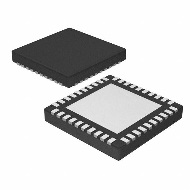


 工商网监
湘ICP备2023018690号
工商网监
湘ICP备2023018690号
