DCR021205, DCR022405
SBVS028D – DECEMBER 2000 – REVISED AUGUST 2021
DCR02 Series, 2-W, 1000-VRMS Isolated, Regulated DC/DC Converter Modules
1 Features
3 Description
•
•
The DCR02 family is a series of high-efficiency,
input-isolated, output-regulated DC/DC converters. In
addition to 2-W nominal, galvanically-isolated output
power capability, this range of converters offers very
low output noise and high accuracy.
•
•
•
•
•
•
•
•
•
•
1-kV isolation (operational): 1-second test
Continuous voltage applied across isolation
barrier: 60 VDC / 42.5 VAC
UL1950 recognized component
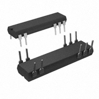
10-pin PDIP and SOP packages
Input voltage: 12 V or 24 V
5-V output voltage
Device-to-device synchronization
400-kHz switching frequency
Short-circuit protection
Thermal protection
High efficiency
125 FITS at 55°C
2 Applications
•
•
•
•
Point-of-use power conversion
Digital interface power
Ground loop elimination
Power-supply noise reduction
The DCR02 family is implemented in standard
molded device packaging, providing standard JEDEC
outlines suitable for high-volume assembly. They
are manufactured using the same technology as
standard device packages, thereby achieving very
high reliability.
WARNING: This product has operational isolation and is intended
for signal isolation only. It must not be used as a part of a safety
isolation circuit requiring reinforced isolation. See definitions in
Section 7.3.
Device Information
PART
NUMBER
DCR02xxxx
(1)
+VS
PACKAGE(1)
BODY SIZE (NOM)
PDIP (10)
22.86 mm × 6.61 mm
SOP (10)
22.86 mm × 6.61 mm
For all available packages, see the orderable addendum at
the end of the datasheet.
VREC
+VOUT
SYNC
Input
Controller
LDO
Regulator
ERROR
ENABLE
-VS
-VOUT
DCR02 Block Diagram
An IMPORTANT NOTICE at the end of this data sheet addresses availability, warranty, changes, use in safety-critical applications,
intellectual property matters and other important disclaimers. PRODUCTION DATA.
�DCR021205, DCR022405
www.ti.com
SBVS028D – DECEMBER 2000 – REVISED AUGUST 2021
Table of Contents
1 Features............................................................................1
2 Applications..................................................................... 1
3 Description.......................................................................1
4 Revision History.............................................................. 2
5 Pin Configuration and Functions...................................3
6 Specifications.................................................................. 4
6.1 Absolute Maximum Ratings........................................ 4
6.2 ESD Ratings............................................................... 4
6.3 Recommended Operating Conditions.........................4
6.4 Thermal Information....................................................4
6.5 Electrical Characteristics.............................................5
6.6 Typical Characteristics................................................ 6
7 Detailed Description........................................................7
7.1 Overview..................................................................... 7
7.2 Functional Block Diagram........................................... 7
7.3 Feature Description.....................................................7
7.4 Device Functional Modes............................................9
8 Application and Implementation.................................. 11
8.1 Application Information..............................................11
8.2 Typical Application.................................................... 13
9 Power Supply Recommendations................................15
10 Layout...........................................................................16
10.1 Layout Guidelines................................................... 16
10.2 Layout Examples.................................................... 16
10.3 Thermal Consideration............................................17
11 Device and Documentation Support..........................18
11.1 Documentation Support.......................................... 18
11.2 Receiving Notification of Documentation Updates.. 18
11.3 Support Resources................................................. 18
11.4 Trademarks............................................................. 18
11.5 Electrostatic Discharge Caution.............................. 18
11.6 Glossary.................................................................. 18
12 Mechanical, Packaging, and Orderable
Information.................................................................... 18
4 Revision History
Changes from Revision C (November 2016) to Revision D (August 2021)
Page
• Updated the numbering format for tables, figures, and cross-references throughout the document. ................1
• Updated Section 1 ............................................................................................................................................. 1
• Added links to Section 2 .................................................................................................................................... 1
• Added Load Regulation plots to Section 6.6 ......................................................................................................6
• Added sentence to Section 7.3.1.3 ....................................................................................................................8
Changes from Revision B (December 2007) to Revision C (November 2016)
Page
• Added ESD Ratings table, Feature Description section, Device Functional Modes, Application and
Implementation section, Power Supply Recommendations section, Layout section, Device and
Documentation Support section, and Mechanical, Packaging, and Orderable Information section................... 1
• Deleted Ordering Information table and Supplemental Ordering Information image; see Package Option
Addendum at the end of the data sheet..............................................................................................................1
• Changed DCR02 PinOut image in Pin Configuration and Functions .................................................................3
• Changed Pin 1 From: VS To: +VS ...................................................................................................................... 3
• Changed Pin 8 From: 0VOUT To: –VOUT .............................................................................................................3
• Changed Pin 9 From: VO To: +VOUT .................................................................................................................. 3
• Changed Pin 17 From: 0VIN To: –VS ..................................................................................................................3
• Deleted Lead temperature (PDIP package), 270°C maximum, from Absolute Maximum Ratings table............ 4
• Added Isolation subsection to the Feature Description ..................................................................................... 7
2
Submit Document Feedback
Copyright © 2021 Texas Instruments Incorporated
Product Folder Links: DCR021205 DCR022405
�DCR021205, DCR022405
www.ti.com
SBVS028D – DECEMBER 2000 – REVISED AUGUST 2021
5 Pin Configuration and Functions
+VS
1
18
SYNC
NC
2
17
-VS
DCR02
VREC
7
12
ERROR
-VOUT
8
11
ENABLE
+VOUT
9
10
DNC
Figure 5-1. NVE or DVS Package 10-Pin PDIP or SOP Top View
Table 5-1. Pin Functions
PIN
NO.
1
NAME
I/O(1)
DESCRIPTION
+VS
I
2
NC
—
No connection
7
VREC
O
Rectified output
8
–VOUT
O
Output ground
9
+VOUT
O
Voltage output
10
DNC
—
Do not connect
11
ENABLE
I
Output voltage enable
12
ERROR
O
Error flag active low
17
–VS
I
Input ground
18
SYNC
I
Synchronization input
(1)
Voltage input
I = input and O = output
Submit Document Feedback
Copyright © 2021 Texas Instruments Incorporated
Product Folder Links: DCR021205 DCR022405
3
�DCR021205, DCR022405
www.ti.com
SBVS028D – DECEMBER 2000 – REVISED AUGUST 2021
6 Specifications
6.1 Absolute Maximum Ratings
over operating free-air temperature range (unless otherwise noted)(1)
MIN
Input voltage
Reflow solder temperature
UNIT
15
DCR022405
29
SOP package (surface temperature of device body or pins)
260
°C
125
°C
Storage temperature, Tstg
(1)
MAX
DCR021205
–60
V
Stresses beyond those listed under Absolute Maximum Ratings may cause permanent damage to the device. These are stress
ratings only, which do not imply functional operation of the device at these or any other conditions beyond those indicated under
Recommended Operating Conditions. Exposure to absolute-maximum-rated conditions for extended periods may affect device
reliability.
6.2 ESD Ratings
VALUE
V(ESD)
(1)
(2)
Electrostatic
discharge
Human-body model (HBM), per ANSI/ESDA/JEDEC
JS-001(1)
UNIT
±1000
Charged-device model (CDM), per JEDEC specification JESD22-C101(2)
V
±250
JEDEC document JEP155 states that 500-V HBM allows safe manufacturing with a standard ESD control process.
JEDEC document JEP157 states that 250-V CDM allows safe manufacturing with a standard ESD control process.
6.3 Recommended Operating Conditions
over operating free-air temperature range (unless otherwise noted)
Input voltage
MIN
NOM
MAX
DCR021205
10.8
12
13.2
DCR022405
21.6
24
26.4
Operating temperature
–40
70
UNIT
V
°C
6.4 Thermal Information
DCR02
THERMAL METRIC(1)
DVS (SOP)
10 PINS
10 PINS
UNIT
RθJA
Junction-to-ambient thermal resistance
60
60
°C/W
RθJC(top)
Junction-to-case (top) thermal resistance
26
26
°C/W
RθJB
Junction-to-board thermal resistance
24
24
°C/W
ψJT
Junction-to-top characterization parameter
7
7
°C/W
ψJB
Junction-to-board characterization parameter
24
24
°C/W
(1)
4
NVE (PDIP)
For more information about traditional and new thermal metrics, see the Semiconductor and IC Package Thermal Metrics application
report.
Submit Document Feedback
Copyright © 2021 Texas Instruments Incorporated
Product Folder Links: DCR021205 DCR022405
�DCR021205, DCR022405
www.ti.com
SBVS028D – DECEMBER 2000 – REVISED AUGUST 2021
6.5 Electrical Characteristics
At TA = +25°C, VS = nominal, IOUT = 10 mA, COUT = 0.1-µF ceramic, and CIN = 2.2-µF ceramic, unless otherwise noted.(1)
PARAMETER
TEST CONDITIONS
MIN
TYP
MAX
UNIT
OUTPUT
Nominal output voltage (+VOUT)
5
Setpoint accuracy
0.5%
Maximum output current
Output short-circuit protected
2%
400
Duration
mA
Infinite
Line regulation
1
Over line and load
10-mA to 400-mA load, over +VS range
1%
Temperature variation
–40°C to 70°C
1%
Ripple and noise
V
DCR0212 ripple, 20−MHz bandwidth, 50% load(1)
18
DCR0212 noise, 100−MHz bandwidth, 50% load(1)
20
DCR0224 ripple, 20−MHz bandwidth, 50% load(1)
18
DCR0224 noise, 100−MHz bandwidth, 50% load(1)
25
DCR022405
12
DCR021205
24
mV/V
2.5%
mVPP
INPUT
Nominal voltage (+VS)
Voltage range
–10%
IO = 0 mA
DCR021205
Supply current
DCR022405
Reflected ripple current
V
10%
15
IO = 10 mA
23
IO = 400 mA
250
IO = 0 mA
15
IO = 10 mA
17
IO = 400 mA
129
20−MHz bandwidth, 100% load(1)
mA
8
mAPP
ISOLATION
Voltage
1-s flash test
Voltage
1
kVrms
dV/dt
500
V/s
30
nA
DC
60
VDC
AC
42.5
VAC
Leakage current
Continuous working voltage
across isolation barrier
Barrier capacitance
25
pF
OUTPUT ENABLE CONTROL
Logic high input voltage
Logic high input current
2
2 < VENABLE < VREG
Logic low input voltage
Logic low input current
VREC
100
–0.2
0 < VENABLE < 0.5
V
nA
0.5
100
V
nA
ERROR FLAG
Logic high open collector leakage
VERROR = 5 V
10
µA
Logic low output voltage
Sinking 2 mA
0.4
V
THERMAL SHUTDOWN
Junction temperature
Temp activated
150
Temp deactivated
130
°C
SYNCHRONIZATION PIN
Internal oscillator frequency
720
External synchronization frequency
720
800
880
kHz
880
kHz
Submit Document Feedback
Copyright © 2021 Texas Instruments Incorporated
Product Folder Links: DCR021205 DCR022405
5
�DCR021205, DCR022405
www.ti.com
SBVS028D – DECEMBER 2000 – REVISED AUGUST 2021
At TA = +25°C, VS = nominal, IOUT = 10 mA, COUT = 0.1-µF ceramic, and CIN = 2.2-µF ceramic, unless otherwise noted.(1)
PARAMETER
TEST CONDITIONS
MIN
External synchronization signal high
External synchronization signal low
TYP
MAX
3
0
0.4
V
3
pF
External capacitance on SYNC pin
(1)
UNIT
2.5
V
Ceramic capacitors, CIN = 2.2 µF, CFILTER = 1 µF, and COUT = 0.1 µF.
100
100
90
90
80
80
70
70
Efficiency (%)
Efficiency (%)
6.6 Typical Characteristics
60
50
40
VIN
10.8 V
11.4 V
12.0 V
12.6 V
13.2 V
30
20
10
60
50
40
VIN
21.6 V
22.8 V
24.0 V
25.2 V
26.4 V
30
20
10
0
0
0
50
100
150
200
250
Output Current (mA)
300
350
0
400
50
100
D001
150
200
250
Output Current (mA)
300
350
400
D002
Figure 6-2. DCR022405 Efficiency vs Output
Current
Figure 6-1. DCR021205 Efficiency versus Output
Current
4.98
5.004
5.002
5
Output Voltage (V)
Output Voltage (V)
4.975
4.97
4.965
4.998
4.996
4.994
4.992
4.99
4.988
4.96
4.986
4.984
4.955
0
50
100
150
200
250
Output Current (mA)
300
350
Figure 6-3. DCR021205 Load Regulation
6
400
0
50
D003
100
150
200
250
Output Current (mA)
300
350
400
D004
Figure 6-4. DCR022405 Load Regulation
Submit Document Feedback
Copyright © 2021 Texas Instruments Incorporated
Product Folder Links: DCR021205 DCR022405
�DCR021205, DCR022405
www.ti.com
SBVS028D – DECEMBER 2000 – REVISED AUGUST 2021
7 Detailed Description
7.1 Overview
The DCR02 series of power modules offer isolation from a regulated power supply operating from 12-V or 24-V
inputs. The DCR02s provide a regulated 5-V output voltage at a nominal output power of 2 W. The DCR02
devices include a low dropout linear regulator internal to the device to achieve a well-regulated output voltage.
The DCR02 devices are specified for operational isolation only. The circuit design uses an advanced BiCMOS
and DMOS process.
7.2 Functional Block Diagram
SYNC
Oscillator
800 kHz
+VS
+VOUT
Divide-by-2
Reset
LDO
Regulator
Power
Stage
Watchdog
Startup
Input
Controller
VREC
ERROR
ENABLE
PSU Thermal
Shutdown
-VS
-VOUT
7.3 Feature Description
7.3.1 Isolation
Underwriters Laboratories (UL)™ defines several classes of isolation that are used in modern power supplies.
Safety extra low voltage (SELV) is defined by UL (UL1950 E199929) as a secondary circuit which is so
designated and protected that under normal and single fault conditions the voltage between any two accessible
parts, or between an accessible part and the equipment earthing terminal for operational isolation does not
exceed steady state 42.5 VRMS or 60 VDC peak.
7.3.1.1 Operation or Functional Isolation
The type of isolation used in the DCR02 products is referred to as operational or functional isolation. Insulated
wire used in the construction of the transformer acts as the primary isolation barrier. A high-potential (hipot),
one-second duration test (dielectric voltage, withstand test) is a production test used to verify that the isolation
barrier is functioning. Products with operational isolation must never be used as an element in a safety-isolation
system.
7.3.1.2 Basic or Enhanced Isolation
Basic or enhanced isolation is defined by specified creepage and clearance limits between the primary and
secondary circuits of the power supply. Basic isolation is the use of an isolation barrier in addition to the
insulated wire in the construction of the transformer. Input and output circuits must also be physically separated
by specified distances.
Submit Document Feedback
Copyright © 2021 Texas Instruments Incorporated
Product Folder Links: DCR021205 DCR022405
7
�DCR021205, DCR022405
www.ti.com
SBVS028D – DECEMBER 2000 – REVISED AUGUST 2021
Note
The DCR02 products do not provide basic or enhanced isolation.
7.3.1.3 Working Voltage
For a device with operational isolation, the continuous working voltage that can be applied across the device in
normal operation must be less than 42.5 VRMS or 60 VDC. Ensure that both input and output voltages maintain
normal SELV limits.
WARNING
Do not use the device as an element of a safety isolation system that exceeds the SELV limit.
If the device is expected to function correctly with more than 42.5 VRMS or 60 VDC applied continuously across
the isolation barrier, then the circuitry on both sides of the barrier must be regarded as operating at an unsafe
voltage, and further isolation or insulation systems must form a barrier between these circuits and any useraccessible circuitry according to safety standard requirements.
7.3.1.4 Isolation Voltage Rating
The terms Hipot test, flash-tested, withstand voltage, proof voltage, dielectric withstand voltage, and isolation
test voltage all relate to the same thing; a test voltage applied for a specified time across a component designed
to provide electrical isolation to verify the integrity of that isolation. TI’s DCR02 series of DC/DC converters are
all 100% production tested at 1.0 kVAC for one second.
7.3.1.5 Repeated High-Voltage Isolation Testing
Repeated high-voltage isolation testing of a barrier component can degrade the isolation capability, depending
on materials, construction, and environment. The DCR02 series of DC/DC converters have toroidal, enameled,
wire isolation transformers with no additional insulation between the primary and secondary windings. While a
device can be expected to withstand several times the stated test voltage, the isolation capability depends on the
wire insulation. Any material, including this enamel (typically polyurethane), is susceptible to eventual chemical
degradation when subject to very-high applied voltages. Therefore, strictly limit the number of high-voltage tests
and repeated high-voltage isolation testing. However, if it is absolutely required, reduce the voltage by 20% from
specified test voltage with a duration limit of one second per test.
7.3.2 Power Stage
The DCR02 series of devices use a push-pull, center-tapped topology. The DCR02 devices switch at 400 kHz
(divide-by-2 from an 800-kHz oscillator). The internal transformer’s output is full wave rectified and filtered by
the external 1-µF ceramic capacitor connected to the VREC pin. An internal low-dropout regulator provides a
well-regulated output voltage over the operating range of the device.
7.3.3 Oscillator and Watchdog
The onboard, 800-kHz oscillator generates the switching frequency through a divide-by-2 circuit. The oscillator
can be synchronized to other DCR02 device circuits or an external source, and is used to minimize system
noise.
A watchdog circuit monitors the operation of the oscillator circuit. The oscillator can be disabled by pulling the
SYNC pin low. When the SYNC pin goes low, the output pins transition into tri-state mode, which occurs within
2 µs.
7.3.4 ERROR Flag
The DCR02 has an ERROR pin which provides a power good flag, as long as the internal regulator is in
regulation. If the ERROR output is required, place a 10-kΩ resistor between the ERROR pin and the output
voltage.
8
Submit Document Feedback
Copyright © 2021 Texas Instruments Incorporated
Product Folder Links: DCR021205 DCR022405
�DCR021205, DCR022405
www.ti.com
SBVS028D – DECEMBER 2000 – REVISED AUGUST 2021
7.3.5 Synchronization
When more than one DC/DC converter is switching in an application, beat frequencies and other electrical
interference can be generated. This interference occurs because of the small variations in switching frequencies
between the DC/DC converters.
The DCR02 series of devices overcome this interference by allowing devices to be synchronized to one
another. Synchronize up to eight devices by connecting the SYNC pins of each device, taking care to minimize
the capacitance of tracking. Stray capacitance (greater than 3 pF) reduces the switching frequency, or can
sometimes stop the oscillator circuit. The maximum recommended voltage applied to the SYNC pin is 3 V.
For an application that uses more than eight synchronized devices use an external device to drive the SYNC
pins. The External Synchronization of the DCP01/02 Series of DC/DC Converters Application Report (SBAA035)
describes this configuration.
Note
During the start-up period, all synchronized devices draw maximum current from the input
simultaneously. A ceramic capacitor must be connected close to each device's input pin. A 2.2-µF
ceramic capacitor is required.
7.3.6 Construction
The basic construction of the DCR02 series of devices is the same as standard integrated circuits. The molded
package contains no substrate. The DCR02 series of devices are constructed using an IC, low dropout linear
regulator, rectifier diodes, and a wound magnetic toroid on a leadframe. Because the package contains no
solder, the devices do not require any special printed-circuit board (PCB) assembly processing. This architecture
results in an isolated DC/DC converter with inherently high reliability.
7.3.7 Decoupling – Ripple Reduction
Due to the very low forward resistance of the DMOS switching transistors, high current demands are placed
upon the input supply for a short time. By using a high-quality, low Equivalent Series Resistance (ESR) ceramic
input capacitor of 2.2-µF, placed close to the IC supply input pins, the effects on the power supply can be
minimized.
The high switching frequency of 400 kHz allows relatively small values of capacitors to be used for filtering
the rectified output voltage. A good-quality, low-ESR, 1-µF ceramic capacitor placed close to the VREC pin and
output ground is required and reduces the ripple. The output at VREC is full wave rectified and produces a ripple
of 800 kHz.
TI recommends that a 0.1-µF, low-ESR ceramic capacitor is connected close to the output pin and ground to
reduce noise on the output. The capacitor values listed are minimum values. If lower ripple is required, the filter
capacitor must be increased in value to 2.2 µF.
As with all switching power supplies, the best performance is obtained with low ESR ceramic capacitors
connected close to the device pins. If low-ESR ceramic capacitors are not used, the ESR generates a voltage
drop when the capacitor is supplying the load power. Often a larger capacitor is chosen for this purpose, when a
low ESR, smaller capacitor would perform as well.
Note
TI does not recommend that the DCR02 be fitted using an IC socket, as this degrades performance.
7.4 Device Functional Modes
7.4.1 Device Disable and Enable
Each of the DCR02 series devices can be disabled or enabled by driving the SYNC pin using an open-drain
CMOS gate. If the SYNC pin is pulled low, the DCR02 becomes disabled. The disable time depends upon the
Submit Document Feedback
Copyright © 2021 Texas Instruments Incorporated
Product Folder Links: DCR021205 DCR022405
9
�DCR021205, DCR022405
SBVS028D – DECEMBER 2000 – REVISED AUGUST 2021
www.ti.com
external loading. The internal disable function is implemented in 2 µs. Removal of the pulldown causes the
DCR02 to be enabled.
Capacitive loading on the SYNC pin must be minimized (≤ 3 pF) to prevent a reduction in the oscillator
frequency. The External Synchronization of the DCP01/02 Series of DC/DC Converters Application Report
(SBAA035) describes disable and enable control circuitry. This document contains information on how to null the
effects of additional capacitance on the SYNC pin. The oscillator’s frequency can be measured at VREC, as this
is the fundamental frequency of the ripple component.
7.4.2 Regulated Output Disable and Enable
The regulated output of the DCR02 can be disabled by pulling the ENABLE pin LOW. Disabling the output
voltage this way still produces a voltage on the VREC pin. When using the ENABLE control, TI recommends
placing a 10-kΩ resistor between the VREC and ENABLE pins. The ENABLE pin only controls the internal linear
regulator.
If disabling the regulated output is not required, pull the ENABLE pin HIGH by shorting it directly to the VREC pin.
This enables the regulated output voltage, thus allowing the output to be controlled from the isolated side.
10
Submit Document Feedback
Copyright © 2021 Texas Instruments Incorporated
Product Folder Links: DCR021205 DCR022405
�DCR021205, DCR022405
www.ti.com
SBVS028D – DECEMBER 2000 – REVISED AUGUST 2021
8 Application and Implementation
Note
Information in the following applications sections is not part of the TI component specification,
and TI does not warrant its accuracy or completeness. TI’s customers are responsible for
determining suitability of components for their purposes, as well as validating and testing their design
implementation to confirm system functionality.
8.1 Application Information
The DCR02 devices offer up to 2 W of isolated, 5-V regulated output power from a 12-V or 24-V input supply.
Applications requiring up to 1-kVrms of operational isolation benefits from the small size and ease-of-use of the
DCR02 family of devices.
8.1.1 DCR02 Single Voltage Output
The DCR02 can be used to provide a single voltage output by connecting the circuit as shown in Figure 8-1. The
ERROR output signal is pulled up to the value of VOUT for the particular DCR02 being used. The value of RERR
depends on the loading on the ERROR line; however, the total load on the ERROR line must not exceed the
value given in the Section 6.5.
The output can be permanently enabled by connecting the ENABLE pin to the VREC pin. The DCR02 can be
enabled remotely by connecting the ENABLE pin to VREC through a pull-up resistor (REN); the value of this
resistor is not critical for the DCR02, because only a small current flows. Switch SW1 can be used to pull
the ENABLE pin low, thus disabling the output. The switching devices can be a bipolar transistor, FET, or a
mechanical device; the main load that it senses is REN.
SYNC
VIN
+VOUT
ERROR
+VS
+VOUT
RERR
10 k
ERROR
VREC
DCR02
CIN
2.2 µF
ENABLE
REN
10 k
SW1
±VS
COUT
0.1 µF
±VOUT
CFILTER
1 µF
±VOUT
Low-ESR, ceramic capacitors are required for CIN, COUT, and CFILTER.
Figure 8-1. DCR02 Single Output Voltage
8.1.2 Generating Two Positive Output Voltages
Two DCR02s can be used to create two +5-V output voltages, as shown in Figure 8-2. The two DCR02s are
connected in self-synchronization, thus locking the oscillators of both devices to a single frequency. The ERROR
and ENABLE facilities can be used in a similar configuration for a single DCR02. The filter capacitors connected
to the VREC pins (CFILTER) must be kept separate from each other and connected in close proximity to the
respective DCR02. If similar output voltages are being used, TI does not recommend that a single filter capacitor
(with an increased capacitance) be used with both VREC pins connected together, because this could result in
the overloading of one of the devices.
Submit Document Feedback
Copyright © 2021 Texas Instruments Incorporated
Product Folder Links: DCR021205 DCR022405
11
�DCR021205, DCR022405
www.ti.com
SBVS028D – DECEMBER 2000 – REVISED AUGUST 2021
VIN
+VOUT
+VS
ERROR
CIN
2.2 µF
+VOUT1
RERR
10 k
ERROR1
VREC
DCR02
ENABLE
CFILTER
1 µF
±VS
SYNC
COUT
0.1 µF
±VOUT
-VOUT
+VOUT
SYNC
VIN
ERROR
+VS
+VOUT2
RERR
10 k
ERROR2
VREC
DCR02
CIN
2.2 µF
±VS
ENABLE
CFILTER
1 µF
COUT
0.1 µF
±VOUT
Low-ESR, ceramic capacitors are required for CIN, COUT, and CFILTER.
Figure 8-2. Generating Two Positive Voltages from Self-Synchronized DCR02s
8.1.3 Generation of Dual Polarity Voltages from Two Self-Synchronized DCR02s
Two DCR02s can be configured to produce a dual polarity supply (that is, ±5 V); the circuit must be connected
as shown in Figure 8-3.
It must be observed that both DCR02s are positive voltage regulators; therefore the ERROR, ENABLE, and
VREC pins are relative to their respective devices, 0 V, and must not be connected together.
VIN
+VOUT
+VS
VPOS O/P
ERROR
CIN
2.2 µF
VREC
DCR02
ENABLE
±VS
SYNC
CFILTER
1 µF
COUT
0.1 µF
±VOUT
0V
+VOUT
SYNC
VIN
ERROR
+VS
VREC
DCR02
CIN
2.2 µF
±VS
ENABLE
CFILTER
1 µF
±VOUT
COUT
0.1 µF
VNEG O/P
Low-ESR, ceramic capacitors are required for CIN, COUT, and CFILTER.
Figure 8-3. Dual Polarity Voltage Generation from Two Self-Synchronized DCR02s
12
Submit Document Feedback
Copyright © 2021 Texas Instruments Incorporated
Product Folder Links: DCR021205 DCR022405
�DCR021205, DCR022405
www.ti.com
SBVS028D – DECEMBER 2000 – REVISED AUGUST 2021
8.2 Typical Application
SYNC
DCR021205
+VOUT = 5V
+VOUT
RERR
10 k
VIN = 12V
+VS
ERROR
CIN
2.2 µF
COUT
0.1 µF
VREC
ENABLE
CFILTER
1.0 µF
±VS
±VOUT
±VOUT
Low-ESR, ceramic capacitors are required for CIN, COUT, and CFILTER.
Figure 8-4. DCR02 Typical Schematic
8.2.1 Design Requirements
For this design example, use the parameters listed in Table 8-1 and follow the design procedure.
Table 8-1. Design Example Parameters
DESIGN PARAMETER
VALUE
Input voltage, VIN
12 V typical
Output voltage, VOUT
5 V regulated
Output current rating
400 mA
Isolation
1000-V operational
8.2.2 Detailed Design Procedure
8.2.2.1 Input Capacitor
For this design, a 2.2-µF, ceramic capacitor is required for the input decoupling capacitor.
8.2.2.2 Output Capacitor
For this design, a 0.1-µF, ceramic capacitor is required for between +VOUT and –VOUT.
8.2.2.3 Filter Capacitor
A high-quality, low-ESR, 1-µF, ceramic capacitor placed close to the VREC pin and output ground is required to
reduce output voltage ripple.
8.2.2.4 ERROR Flag
Place a 10-kΩ resistor between the ERROR pin and the output voltage to provide a power good signal when the
internal regulator is in regulation.
Submit Document Feedback
Copyright © 2021 Texas Instruments Incorporated
Product Folder Links: DCR021205 DCR022405
13
�DCR021205, DCR022405
www.ti.com
SBVS028D – DECEMBER 2000 – REVISED AUGUST 2021
8.2.3 Application Curves
100
90
80
Efficiency (%)
70
60
50
40
VIN
10.8 V
11.4 V
12.0 V
12.6 V
13.2 V
30
20
10
0
0
50
100
150
200
250
Output Current (mA)
300
350
400
D001
Figure 8-5. DCR021205 Efficiency versus Output Current
14
Submit Document Feedback
Copyright © 2021 Texas Instruments Incorporated
Product Folder Links: DCR021205 DCR022405
�DCR021205, DCR022405
www.ti.com
SBVS028D – DECEMBER 2000 – REVISED AUGUST 2021
9 Power Supply Recommendations
The DCR02 is a switching power supply, and as such can place high peak current demands on the input supply.
To avoid the supply falling momentarily during the fast switching pulses, ground and power planes must be
used to connect the power to the input of DCR02. If this connection is not possible, then the supplies must be
connected in a star formation with the traces made as wide as possible.
Submit Document Feedback
Copyright © 2021 Texas Instruments Incorporated
Product Folder Links: DCR021205 DCR022405
15
�DCR021205, DCR022405
www.ti.com
SBVS028D – DECEMBER 2000 – REVISED AUGUST 2021
10 Layout
10.1 Layout Guidelines
Carefully consider the layout of the PCB in order for the best results to be obtained.
Input and output power and ground planes provide a low-impedance path for the input and output power. For the
output, the positive and negative voltage outputs conduct through wide traces to minimize losses.
A good-quality, low-ESR, ceramic capacitor placed as close as practical across the input reduces reflected ripple
and ensure a smooth start-up.
A good-quality, low-ESR, ceramic capacitor placed as close as practical across the rectifier output terminal and
output ground gives the best ripple and noise performance.
The location of the decoupling capacitors in close proximity to their respective pins ensures low losses due to
the effects of stray inductance, thus improving the ripple performance. This location is of particular importance
to the input decoupling capacitor, because this capacitor supplies the transient current associated with the fast
switching waveforms of the power drive circuits.
If the SYNC pin is being used, the tracking between device SYNC pins must be short to avoid stray capacitance.
Never connect a capacitor to the SYNC pin. If the SYNC pin is not being used it is advisable to place a guard
ring (connected to input ground) around this pin to avoid any noise pickup. Ensure that no other trace is in close
proximity to this trace SYNC trace to decrease the stray capacitance on this pin. The stray capacitance affects
the performance of the oscillator.
Figure 10-1 and Figure 10-2 show a typical layout for the SOP package DCR02 device. The layout shows proper
placement of capacitors and power planes. Figure 10-3 shows a schematic for a single DCR02, SOP package
device.
10.2 Layout Examples
U1
+VS
SYNC
-VS
+VS
SYNC
-VS
C1
C2
VREC
ERROR
VREC
ENABLE
+VOUT
C3
Figure 10-1. PCB Layout Example, ComponentSide View
16
ENABLE
-VOUT
-VOUT
+VOUT
ERROR
Figure 10-2. PCB Layout Example, NonComponent-Side View
Submit Document Feedback
Copyright © 2021 Texas Instruments Incorporated
Product Folder Links: DCR021205 DCR022405
�DCR021205, DCR022405
www.ti.com
SBVS028D – DECEMBER 2000 – REVISED AUGUST 2021
DCR02
+VS
1
U1
+VS
C1
SYNC 18
-VS
17 ±VS
ERROR 12
VREC
7
VREC
C2
ENABLE 11
-VOUT
8
±VOUT
9
+VOUT
C3
+VOUT
Figure 10-3. DCR02 PCB Schematic, U Package
10.3 Thermal Consideration
Due to the high power density of this device, it is advisable to provide a ground plane on the output. The output
regulator is mounted on a copper leadframe, and a ground plane serves as an efficient heatsink.
Submit Document Feedback
Copyright © 2021 Texas Instruments Incorporated
Product Folder Links: DCR021205 DCR022405
17
�DCR021205, DCR022405
www.ti.com
SBVS028D – DECEMBER 2000 – REVISED AUGUST 2021
11 Device and Documentation Support
11.1 Documentation Support
11.1.1 Related Documentation
For related documentation see the following:
Texas Instruments, External Synchronization of the DCP01/02 Series of DC/DC Converters (SBAA035)
11.2 Receiving Notification of Documentation Updates
To receive notification of documentation updates, navigate to the device product folder on ti.com. Click on
Subscribe to updates to register and receive a weekly digest of any product information that has changed. For
change details, review the revision history included in any revised document.
11.3 Support Resources
TI E2E™ support forums are an engineer's go-to source for fast, verified answers and design help — straight
from the experts. Search existing answers or ask your own question to get the quick design help you need.
Linked content is provided "AS IS" by the respective contributors. They do not constitute TI specifications and do
not necessarily reflect TI's views; see TI's Terms of Use.
11.4 Trademarks
Underwriters Laboratories (UL)™ is a trademark of UL LLC.
TI E2E™ is a trademark of Texas Instruments.
All trademarks are the property of their respective owners.
11.5 Electrostatic Discharge Caution
This integrated circuit can be damaged by ESD. Texas Instruments recommends that all integrated circuits be handled
with appropriate precautions. Failure to observe proper handling and installation procedures can cause damage.
ESD damage can range from subtle performance degradation to complete device failure. Precision integrated circuits may
be more susceptible to damage because very small parametric changes could cause the device not to meet its published
specifications.
11.6 Glossary
TI Glossary
This glossary lists and explains terms, acronyms, and definitions.
12 Mechanical, Packaging, and Orderable Information
The following pages include mechanical, packaging, and orderable information. This information is the most
current data available for the designated devices. This data is subject to change without notice and revision of
this document. For browser-based versions of this data sheet, refer to the left-hand navigation.
18
Submit Document Feedback
Copyright © 2021 Texas Instruments Incorporated
Product Folder Links: DCR021205 DCR022405
�PACKAGE OPTION ADDENDUM
www.ti.com
10-Dec-2020
PACKAGING INFORMATION
Orderable Device
Status
(1)
Package Type Package Pins Package
Drawing
Qty
Eco Plan
(2)
Lead finish/
Ball material
MSL Peak Temp
Op Temp (°C)
(3)
Device Marking
(4/5)
(6)
DCR021205P
ACTIVE
PDIP
NVE
10
20
RoHS &
Non-Green
NIPDAU
N / A for Pkg Type
-40 to 70
DCR021205P
DCR021205P-U
ACTIVE
SOP
DVS
10
20
RoHS &
Non-Green
NIPDAU
Level-3-260C-168 HR
-40 to 70
DCR021205P-U
DCR022405P
ACTIVE
PDIP
NVE
10
20
RoHS &
Non-Green
NIPDAU
N / A for Pkg Type
-40 to 70
DCR022405P
DCR022405P-U
ACTIVE
SOP
DVS
10
20
RoHS &
Non-Green
NIPDAU
Level-3-260C-168 HR
-40 to 70
DCR022405P-U
DCR022405P-U/700
ACTIVE
SOP
DVS
10
700
RoHS &
Non-Green
NIPDAU
Level-3-260C-168 HR
0 to 0
DCR022405P-U
(1)
The marketing status values are defined as follows:
ACTIVE: Product device recommended for new designs.
LIFEBUY: TI has announced that the device will be discontinued, and a lifetime-buy period is in effect.
NRND: Not recommended for new designs. Device is in production to support existing customers, but TI does not recommend using this part in a new design.
PREVIEW: Device has been announced but is not in production. Samples may or may not be available.
OBSOLETE: TI has discontinued the production of the device.
(2)
RoHS: TI defines "RoHS" to mean semiconductor products that are compliant with the current EU RoHS requirements for all 10 RoHS substances, including the requirement that RoHS substance
do not exceed 0.1% by weight in homogeneous materials. Where designed to be soldered at high temperatures, "RoHS" products are suitable for use in specified lead-free processes. TI may
reference these types of products as "Pb-Free".
RoHS Exempt: TI defines "RoHS Exempt" to mean products that contain lead but are compliant with EU RoHS pursuant to a specific EU RoHS exemption.
Green: TI defines "Green" to mean the content of Chlorine (Cl) and Bromine (Br) based flame retardants meet JS709B low halogen requirements of


 工商网监
湘ICP备2023018690号
工商网监
湘ICP备2023018690号
