Product
Folder
Order
Now
Support &
Community
Tools &
Software
Technical
Documents
DLP4500
DLPS151 – JANUARY 2019
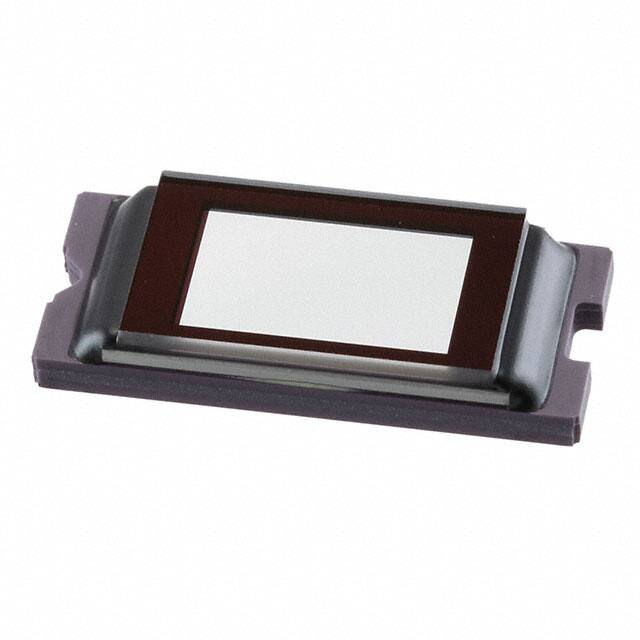
DLP4500 .45 WXGA DMD
1 Features
•
1
•
•
•
•
0.45-Inch Diagonal Micromirror Array
– 912 × 1140 Resolution Array (>1 Million
Micromirrors)
– Diamond Array Orientation Supports Side
Illumination for Simplified, Efficient Optics
Designs
– Capable of WXGA Resolution Display
– 7.6-µm Micromirror Pitch
– ±12° Tilt Angle
– 5-µs Micromirror Crossover Time
Highly Efficient Steering of Visible Light
– Window Transmission Efficiency 96% Nominal
(420 to 700 nm, Single Pass Through Two
Window Surfaces)
– Polarization-Independent Aluminum
Micromirrors
– Array Fill Factor 92% (Nominal)
Dedicated DLPC350 Controller for Reliable
Operation
– Binary Pattern Rates Up to 4 kHz
– Pattern Sequence Mode for Control Over Each
Micromirror in Array
Integrated Micromirror Driver Circuitry
9.1-mm × 20.7-mm for Portable Instruments
– FQE Package With Simple Connector
Interface
– FQD Package With Enhanced Thermal
Interface
2 Applications
•
Machine Vision
– 3-D Depth Measurement
– Robotic Guidance
•
•
•
•
•
•
– Inline Surface Inspection
– Pick and Place
– 3-D Capture
– Defect Rejection
Medical Instruments
– 3-D Dental Scanners
– Vascular Imaging
3-D Biometrics
– Fingerprint Identification
– Facial Recognition
Virtual Gauges
Augmented Reality
Interactive Display
Microscopes
3 Description
The DLP4500 digital micromirror device (DMD) acts
as a spatial light modulator (SLM) to steer visible light
and create patterns with speed, precision, and
efficiency. Featuring high resolution and high
brightness in a compact form factor, the DLP4500
DMD is well-suited for very accurate, portable 3D
machine vision and display solutions used in
industrial, medical, and security applications.
Device Information
PART NUMBER
PACKAGE
LCCC (80) (2)
DLP4500
LCCC (98)
(3)
(1)
THERMAL
INTERFACE AREA
None
7 mm x 7 mm
(1) For all available packages, see the orderable addendum at
the end of the data sheet.
(2) FQE package (Series-241) drawing. See DLP® Series-241
DMD and System Mounting Concepts for more information.
(3) FQD package (Series-310) drawing. See DLP® Series-310
DMD and System Mounting Concepts for more information.
Simplified Application
DC Power
RGB Interface
LED Drivers
LEDs
LVDS Interface
USB Interface
Light Sensor
2
DLPC350
I C Interface
JTAG
GPIO Interface
Oscillator
DDR Interface
DLP4500
1
An IMPORTANT NOTICE at the end of this data sheet addresses availability, warranty, changes, use in safety-critical applications,
intellectual property matters and other important disclaimers. PRODUCTION DATA.
�DLP4500
DLPS151 – JANUARY 2019
www.ti.com
Table of Contents
1
2
3
4
5
6
7
7.1
7.2
7.3
7.4
7.5
7.6
7.7
7.8
7.9
7.10
7.11
8
8.4 Device Functional Modes........................................ 27
8.5 Micromirror Array Temperature Calculation............ 27
8.6 Micromirror Landed-on/Landed-Off Duty Cycle ...... 30
Features .................................................................. 1
Applications ........................................................... 1
Description ............................................................. 1
Revision History..................................................... 2
Chipset Component Usage Specification ........... 3
Pin Configuration and Functions ......................... 4
Specifications....................................................... 12
9
Applications and Implementation ...................... 33
9.1 Application Information............................................ 33
9.2 Typical Application .................................................. 33
10 Power Supply Recommendations ..................... 38
10.1 Power Supply Sequencing Requirements ............ 38
10.2 DMD Power Supply Power-Up Procedure ............ 38
10.3 DMD Power Supply Power-Down Procedure ....... 38
Absolute Maximum Ratings ................................... 12
Storage Conditions.................................................. 12
ESD Ratings .......................................................... 12
Recommended Operating Conditions..................... 13
Thermal Information ................................................ 15
Electrical Characteristics......................................... 16
Timing Requirements .............................................. 17
System Mounting Interface Loads .......................... 19
Micromirror Array Physical Characteristics ............. 21
Micromirror Array Optical Characteristics ............. 22
Typical Characteristics .......................................... 23
11 Layout................................................................... 40
11.1 Layout Guidelines ................................................. 40
11.2 Layout Example .................................................... 45
12 Device and Documentation Support ................. 50
12.1
12.2
12.3
12.4
12.5
12.6
Detailed Description ............................................ 24
8.1 Overview ................................................................. 24
8.2 Functional Block Diagram ....................................... 24
8.3 Feature Description................................................. 25
Device Support......................................................
Documentation Support ........................................
Community Resources..........................................
Trademarks ...........................................................
Electrostatic Discharge Caution ............................
Glossary ................................................................
50
51
51
51
51
52
13 Mechanical, Packaging, and Orderable
Information ........................................................... 52
4 Revision History
NOTE: Page numbers for previous revisions may differ from page numbers in the current version.
2
DATE
REVISION
NOTES
January 2019
*
Initial release.
Submit Documentation Feedback
Copyright © 2019, Texas Instruments Incorporated
Product Folder Links: DLP4500
�DLP4500
www.ti.com
DLPS151 – JANUARY 2019
5 Chipset Component Usage Specification
NOTE
TI assumes no responsibility for image quality artifacts or DMD failures caused by optical
system operating conditions exceeding limits described previously.
The DLP4500 is a component of one or more DLP® chipsets. Reliable function and operation of the DLP4500
requires that it be used in conjunction with the other components of the applicable DLP chipset, including those
components that contain or implement TI DMD control technology. TI DMD control technology is the TI
technology and devices for operating or controlling a DLP DMD.
Submit Documentation Feedback
Copyright © 2019, Texas Instruments Incorporated
Product Folder Links: DLP4500
3
�DLP4500
DLPS151 – JANUARY 2019
www.ti.com
6 Pin Configuration and Functions
FQE Package
LCCC (80)
Bottom View
4
Submit Documentation Feedback
Copyright © 2019, Texas Instruments Incorporated
Product Folder Links: DLP4500
�DLP4500
www.ti.com
DLPS151 – JANUARY 2019
Connector Pins for FQE
PIN
NAME
NO.
TYPE
SIGNAL
DATA RATE
(1)
INTERNAL
TERMINATION
DESCRIPTION
TRACE (mm)
(2)
DATA INPUTS
DATA(0)
C12
Input
LVCMOS
DDR
none
Input data bus, bit 0, LSB
8.11
DATA(1)
C10
Input
LVCMOS
DDR
none
Input data bus, bit 1
7.82
DATA(2)
C9
Input
LVCMOS
DDR
none
Input data bus, bit 2
7.88
DATA(3)
C7
Input
LVCMOS
DDR
none
Input data bus, bit 3
7.84
DATA(4)
C4
Input
LVCMOS
DDR
none
Input data bus, bit 4
8.10
DATA(5)
C6
Input
LVCMOS
DDR
none
Input data bus, bit 5
7.89
DATA(6)
C3
Input
LVCMOS
DDR
none
Input data bus, bit 6
7.87
DATA(7)
C13
Input
LVCMOS
DDR
none
Input data bus, bit 7
7.84
DATA(8)
C15
Input
LVCMOS
DDR
none
Input data bus, bit 8
8.13
DATA(9)
C16
Input
LVCMOS
DDR
none
Input data bus, bit 9
8.00
DATA(10)
C18
Input
LVCMOS
DDR
none
Input data bus, bit 10
8.12
DATA(11)
C19
Input
LVCMOS
DDR
none
Input data bus, bit 11
8.08
DATA(12)
C21
Input
LVCMOS
DDR
none
Input data bus, bit 12
9.27
DATA(13)
C22
Input
LVCMOS
DDR
none
Input data bus, bit 13
9.47
DATA(14)
D22
Input
LVCMOS
DDR
none
Input data bus, bit 14
9.46
DATA(15)
D21
Input
LVCMOS
DDR
none
Input data bus, bit 15
8.73
DATA(16)
D19
Input
LVCMOS
DDR
none
Input data bus, bit 16
8.10
DATA(17)
D4
Input
LVCMOS
DDR
none
Input data bus, bit 17
8.02
DATA(18)
D9
Input
LVCMOS
DDR
none
Input data bus, bit 18
8.07
DATA(19)
D10
Input
LVCMOS
DDR
none
Input data bus, bit 19
7.91
DATA(20)
D6
Input
LVCMOS
DDR
none
Input data bus, bit 20
8.52
DATA(21)
D16
Input
LVCMOS
DDR
none
Input data bus, bit 21
9.10
DATA(22)
D7
Input
LVCMOS
DDR
none
Input data bus, bit 22
8.00
DATA(23)
D15
Input
LVCMOS
DDR
none
Input data bus, bit 23, MSB
8.61
DCLK
D13
Input
LVCMOS
DDR
none
Input data bus clock
8.63
DATA CONTROL INPUTS
LOADB
D12
Input
LVCMOS
DDR
none
Parallel-data load enable
8.65
TRC
D3
Input
LVCMOS
DDR
none
Input-data toggle-rate control
4.67
SCTRL
D18
Input
LVCMOS
DDR
none
Serial control bus
9.40
6.56
SAC_BUS
D33
Input
LVCMOS
—
none
Stepped address-control serialbus data
SAC_CLK
D29
Input
LVCMOS
—
none
Stepped address-control serial
bus clock
8.07
MIRROR RESET CONTROL INPUTS
DRC_BUS
C29
Input
LVCMOS
—
none
DMD reset-control serial bus
8.24
C33
Input
LVCMOS
—
none
Active-low output enable signal
for internal DMD reset driver
circuitry
4.43
DRC_OE
DRC_STROBE
C36
Input
LVCMOS
—
none
Strobe signal for DMD reset
control inputs
9.20
(1)
(2)
(a) DDR = Double data rate
(b) SDR = Single data rate
(c) Refer to Timing Requirements for specifications and relationships.
Net trace lengths inside the package:
(a) Relative dielectric constant for the FQE package is 9.8.
(b) Propagation speed = 11.8 / √(9.8) = 3.769 inches/ns.
(c) Propagation delay = 0.265 ns/inch = 265 ps/inch = 10.43 ps/mm.
Submit Documentation Feedback
Copyright © 2019, Texas Instruments Incorporated
Product Folder Links: DLP4500
5
�DLP4500
DLPS151 – JANUARY 2019
www.ti.com
Connector Pins for FQE (continued)
PIN
NAME
POWER INPUTS
NO.
TYPE
C31
Power
VBIAS
C32
Power
VOFFSET
D25
Power
VOFFSET
D26
Power
VRESET
D31
Power
VRESET
D32
Power
VREF
C25
Power
VREF
C26
Power
VCC
C1
Power
VCC
C2
Power
VCC
C34
Power
VCC
C35
Power
VCC
C37
Power
VCC
C38
Power
VCC
C39
Power
VCC
C40
Power
VCC
D1
Power
VCC
D2
Power
VCC
D34
Power
VCC
D35
Power
VCC
D37
Power
VCC
D38
Power
VCC
D39
Power
VCC
D40
Power
6
DATA RATE
(1)
INTERNAL
TERMINATION
DESCRIPTION
TRACE (mm)
(2)
(3)
VBIAS
(3)
SIGNAL
none
Mirror-reset bias voltage
none
Mirror-reset offset voltage
none
Mirror-reset voltage
none
Power supply for low-voltage
CMOS double-data-rate (DDR)
interface
none
Power supply for LVCMOS logic
The following power supplies are all required to operate the DMD: VSS, VCC, VOFFSET, VBIAS, VRESET.
Submit Documentation Feedback
Copyright © 2019, Texas Instruments Incorporated
Product Folder Links: DLP4500
�DLP4500
www.ti.com
DLPS151 – JANUARY 2019
Connector Pins for FQE (continued)
PIN
NAME
NO.
TYPE
VSS
C5
Power
VSS
C8
Power
VSS
C11
Power
VSS
C14
Power
VSS
C17
Power
VSS
C20
Power
VSS
C23
Power
VSS
C24
Power
VSS
C27
Power
VSS
C28
Power
VSS
C30
Power
VSS
D5
Power
VSS
D8
Power
VSS
D11
Power
VSS
D14
Power
VSS
D17
Power
VSS
D20
Power
VSS
D23
Power
VSS
D24
Power
VSS
D27
Power
VSS
D28
Power
VSS
D30
Power
SIGNAL
DATA RATE
(1)
INTERNAL
TERMINATION
DESCRIPTION
none
Ground – Common return for all
power inputs
TRACE (mm)
(2)
Pin Configuration and Functions – Test Pads for FQE Package
NAME
PIN
SIGNAL
DESCRIPTION
Test pads
Do not connect
A1 thru A25
B1 thru B25
UNUSED
D36
E1 thru E25
F1 thru F25
Submit Documentation Feedback
Copyright © 2019, Texas Instruments Incorporated
Product Folder Links: DLP4500
7
�DLP4500
DLPS151 – JANUARY 2019
www.ti.com
FQD Package
LCCC (98)
Bottom View
8
Submit Documentation Feedback
Copyright © 2019, Texas Instruments Incorporated
Product Folder Links: DLP4500
�DLP4500
www.ti.com
DLPS151 – JANUARY 2019
Connector Pins for FQD
PIN
NAME
NO.
TYPE
SIGNAL
DATA RATE
(1)
INTERNAL
TERMINATION
DESCRIPTION
PACKAGE NET
LENGTH (mm)
(2)
DATA INPUTS
DATA(0)
A1
Input
LVCMOS
DDR
none
Input data bus, bit 0, LSB
3.77
DATA(1)
A2
Input
LVCMOS
DDR
none
Input data bus, bit 1
3.77
DATA(2)
A3
Input
LVCMOS
DDR
none
Input data bus, bit 2
3.73
DATA(3)
A4
Input
LVCMOS
DDR
none
Input data bus, bit 3
3.74
DATA(4)
B1
Input
LVCMOS
DDR
none
Input data bus, bit 4
3.79
DATA(5)
B3
Input
LVCMOS
DDR
none
Input data bus, bit 5
3.75
DATA(6)
C1
Input
LVCMOS
DDR
none
Input data bus, bit 6
3.72
DATA(7)
C3
Input
LVCMOS
DDR
none
Input data bus, bit 7
3.75
DATA(8)
C4
Input
LVCMOS
DDR
none
Input data bus, bit 8
3.78
DATA(9)
D1
Input
LVCMOS
DDR
none
Input data bus, bit 9
3.75
DATA(10)
D4
Input
LVCMOS
DDR
none
Input data bus, bit 10
3.77
DATA(11)
E1
Input
LVCMOS
DDR
none
Input data bus, bit 11
3.75
DATA(12)
E4
Input
LVCMOS
DDR
none
Input data bus, bit 12
3.71
DATA(13)
F1
Input
LVCMOS
DDR
none
Input data bus, bit 13
3.76
DATA(14)
F3
Input
LVCMOS
DDR
none
Input data bus, bit 14
3.73
DATA(15)
G1
Input
LVCMOS
DDR
none
Input data bus, bit 15
3.72
DATA(16)
G2
Input
LVCMOS
DDR
none
Input data bus, bit 16
3.77
DATA(17)
G4
Input
LVCMOS
DDR
none
Input data bus, bit 17
3.73
DATA(18)
H1
Input
LVCMOS
DDR
none
Input data bus, bit 18
3.74
DATA(19)
H2
Input
LVCMOS
DDR
none
Input data bus, bit 19
3.76
DATA(20)
H4
Input
LVCMOS
DDR
none
Input data bus, bit 20
3.70
DATA(21)
J1
Input
LVCMOS
DDR
none
Input data bus, bit 21
3.77
DATA(22)
J3
Input
LVCMOS
DDR
none
Input data bus, bit 22
3.76
DATA(23)
J4
Input
LVCMOS
DDR
none
Input data bus, bit 23, MSB
3.77
DCLK
K1
Input
LVCMOS
DDR
none
Input data bus clock
3.74
DATA CONTROL INPUTS
LOADB
K2
Input
LVCMOS
DDR
none
Parallel-data load enable
3.74
TRC
K4
Input
LVCMOS
DDR
none
Input-data toggle rate control
4.70
SCTRL
K3
Input
LVCMOS
DDR
none
Serial-control bus
3.75
3.77
SAC_BUS
C20
Input
LVCMOS
—
none
Stepped address-control serialbus data
SAC_CLK
C22
Input
LVCMOS
—
none
Stepped address-control serialbus clock
1.49
LVCMOS
—
none
DMD reset-control serial bus
3.73
3.74
3.73
MIRROR RESET CONTROL INPUTS
DRC_BUS
B21
Input
DRC_OE
A20
Input
LVCMOS
—
none
Active-low output enable signal
for internal DMD reset driver
circuitry
DRC_STROBE
A22
Input
LVCMOS
—
none
Strobe signal for DMD resetcontrol inputs
(1)
(2)
(a) DDR = Double data rate
(b) SDR = Single data rate
(c) Refer to Timing Requirements for specifications and relationships.
Net trace lengths inside the package:
(a) Relative dielectric constant for the FQD ceramic package is 9.8.
(b) Propagation speed = 11.8 / sqrt(9.8) = 3.769 inches/ns.
(c) Propagation delay = 0.265 ns/inch = 265 ps/inch = 10.43 ps/mm.
Submit Documentation Feedback
Copyright © 2019, Texas Instruments Incorporated
Product Folder Links: DLP4500
9
�DLP4500
DLPS151 – JANUARY 2019
www.ti.com
Connector Pins for FQD (continued)
PIN
NAME
POWER INPUTS
NO.
TYPE
C19
Power
VBIAS
D19
Power
VOFFSET
A19
Power
VOFFSET
K19
Power
VRESET
E19
Power
VRESET
F19
Power
VREF
B19
Power
VREF
J19
Power
VCC
B22
Power
VCC
C2
Power
VCC
D21
Power
VCC
E2
Power
VCC
E20
Power
VCC
E22
Power
VCC
F21
Power
VCC
G3
Power
VCC
G19
Power
VCC
G20
Power
VCC
G22
Power
VCC
H19
Power
VCC
H21
Power
VCC
J20
Power
VCC
J22
Power
VCC
K21
Power
10
DATA RATE
(1)
INTERNAL
TERMINATION
DESCRIPTION
PACKAGE NET
LENGTH (mm)
(2)
(3)
VBIAS
(3)
SIGNAL
Mirror-reset bias voltage
Mirror-reset offset voltage
Mirror-reset voltage
Power supply for LVCMOS
double-data-rate (DDR)
interface
Power supply for LVCMOS logic
The following power supplies are all required to operate the DMD: VSS, VCC, VOFFSET, VBIAS, VRESET.
Submit Documentation Feedback
Copyright © 2019, Texas Instruments Incorporated
Product Folder Links: DLP4500
�DLP4500
www.ti.com
DLPS151 – JANUARY 2019
Connector Pins for FQD (continued)
PIN
NAME
NO.
TYPE
VSS
A21
Power
VSS
B2
Power
VSS
B4
Power
VSS
B20
Power
VSS
C21
Power
VSS
D2
Power
VSS
D3
Power
VSS
D20
Power
VSS
D22
Power
VSS
E3
Power
VSS
E21
Power
VSS
F2
Power
VSS
F4
Power
VSS
F20
Power
VSS
F22
Power
VSS
G21
Power
VSS
H3
Power
VSS
H20
Power
VSS
H22
Power
VSS
J2
Power
VSS
J21
Power
VSS
K20
Power
SIGNAL
DATA RATE
(1)
INTERNAL
TERMINATION
DESCRIPTION
PACKAGE NET
LENGTH (mm)
(2)
Ground – Common return for all
power inputs
Pin Configuration and Functions – Test Pads for FQD Package
NAME
PIN
SIGNAL
DESCRIPTION
UNUSED
A5, A18, B5, B18, C5, C18, D5, D18, E5,
E18, F5, F18, G5, G18, H5, H18, J5, J18,
K22
Test pads
Do not connect
Submit Documentation Feedback
Copyright © 2019, Texas Instruments Incorporated
Product Folder Links: DLP4500
11
�DLP4500
DLPS151 – JANUARY 2019
www.ti.com
7 Specifications
7.1 Absolute Maximum Ratings
over operating free-air temperature range (unless otherwise noted)
SUPPLY VOLTAGES
(1)
MIN
MAX
UNIT
(2)
VCC
Supply voltage for LVCMOS core logic
–0.5
4
V
VREF
Supply voltage for LVCMOS DDR interface
–0.5
4
V
VOFFSET
Supply voltage for high voltage CMOS and micromirror electrode
–0.5
8.75
V
Supply voltage for micromirror electrode
–0.5
17
V
Supply voltage for micromirror electrode
–11
0.5
V
8.75
V
VREF + 0.5
V
VBIAS
(3)
VRESET
|VBIAS - VOFFSET|
(3)
INPUT VOLTAGES
(2)
Supply voltage delta (absolute value)
Input voltage to all other input pins
–0.5
INPUT CURRENTS
Current required from a high-level output
VOH = 1.4 V
–9
mA
Current required from a low-level output
VOL = 0.4 V
18
mA
80
120
MHz
–20
90
°C
–40
90
°C
CLOCKS
fCLK
DCLK clock frequency
ENVIRONMENTAL
Case temperature - operational
TCASE
(4)
Case temperature - non-operational
TDP
(4)
Dew Point (operation and non-operational)
Operating Relative Humidity (non-condensing)
(1)
(2)
(3)
(4)
0
81
°C
95
%RH
Stresses beyond those listed under Absolute Maximum Ratings may cause permanent damage to the device. These are stress ratings
only, and functional operation of the device is not implied at these or any conditions beyond those indicated under. Exposure above
Recommended Operating Conditions for extended periods may affect device reliability.
All voltage values are referenced to common ground VSS. Supply voltages VCC, VREF, VOFFSET, VBIAS, and VRESET are all
required for proper DMD operation. VSS must also be connected.
To prevent excess current, the supply voltage delta |VBIAS – VOFFSET| must be less than the specified limit.
DMD Temperature is the worst-case of any test point shown in Figure 9 or Figure 10, or the active array as calculated by the
Micromirror Array Temperature Calculation, or any point along the Window Edge as defined in Figure 9 or Figure 10. The locations of
thermal test point TP2 is intended to measure the highest window edge temperature. If a particular application causes another point on
the window edge to be at a higher temperature, a test point should be added to that location.
7.2 Storage Conditions
applicable before the DMD is installed in the final product
Storage temperature
Storage humidity, non-condensing
Tstg
(1)
(2)
(3)
(1)
MIN
MAX
UNIT
–40
85
°C
0
(1)
95%
RH
Long-term storage dew point
(1) (2)
24
°C
Short-term storage dew point
(1) (3)
28
°C
As a best practice, TI recommends storing the DMD in a temperature and humidity controlled environment.
Long-term is defined as the average over the usable life.
Short-term is defined as 0.5 V/ns and