DP83822HF, DP83822IF, DP83822H, DP83822I
SNLS505F – JULY 2016 – REVISED JUNE 2021
DP83822 Robust, Low Power 10/100 Mbps Ethernet Physical Layer Transceiver
1 Features
3 Description
•
Ideal for harsh industrial environments, the DP83822
is an ultra-robust, low-power single-port 10/100 Mbps
Ethernet PHY. It provides all physical layer functions
needed to transmit and receive data over standard
twisted-pair cables, or connect to an external fiber
optic transceiver. Additionally, the DP83822 provides
flexibility to connect to a MAC through a standard MII,
RMII, or RGMII interface.
•
•
•
•
•
2 Applications
The DP83822 offers an innovative and robust
approach for reducing power consumption through
EEE, WoL and other programmable energy savings
modes.
The DP83822 is a feature rich and pin-to-pin
upgradeable option for the TLK105, TLK106,
TLK105L and TLK106L 10/100 Mbps Ethernet PHYs.
The DP83822 comes in a 32-pin 5.00-mm × 5.00-mm
VQFN package.
Device Information
Motor drives
Factory automation, robotics and motion control
Grid infrastructure
Building automation
Industrial Ethernet fieldbus
Real Time Industrial Ethernet Applications such as
ProfiNET®
PART NUMBER
PACKAGE (1)
BODY SIZE (NOM)
DP83822HF
VQFN (32)
5.00 mm × 5.00 mm
DP83822H
VQFN (32)
5.00 mm × 5.00 mm
DP83822IF
VQFN (32)
5.00 mm × 5.00 mm
DP83822I
VQFN (32)
5.00 mm × 5.00 mm
(1)
For all available packages, see the orderable addendum at
the end of the data sheet.
100BASE-FX
MAC
Capacitors
MII
RMII
RGMII
DP83822
10/100 Mbps
Ethernet PHY
10BASE-Te
100BASE-TX
Magnetics
•
•
•
•
•
•
The DP83822 offers integrated cable diagnostic tools,
built-in self-test, and loopback capabilities for ease
of use. It supports multiple industrial fieldbuses with
its fast link-down detection as well as Auto-MDIX in
forced modes.
Fiber Optic
Transceiver
•
•
Ultra-robust 10/100Mbs PHY
– IEC 6100-4-2 ESD: +/- 8KV contact discharge
– IEC 6100-4-4 EFT: Class A at 4KV
– CISPR 22 conducted emissions : Class B
– CISPR 22 radiated emissions : Class B
– Operating temperature: -40C to 125C
MAC interfaces: RGMII / RMII / MII
IEEE 802.3u compliant: 100BASE-FX, 100BASETX and 10BASE-Te
Flexible supply options
– Low power single supply options
• 1.8V AVD < 120 mW
• 3.3-V AVD < 220 mW
– Available I/O voltages : 3.3V/2.5V/1.8V
Power saving features
– Energy efficient Ethernet (EEE) IEEE 802.3az
– WoL (Wake-on-LAN) support with magic packet
detection
– Programmable energy savings modes
Start of frame detect for IEEE 1588 time stamp
Diagnostic tools: Cable diagnostics, BIST (Built-in
self-test), loopback, rapid link-down detection
Auto-crossover in force modes
25-MHz / 50-MHz
Clock Source
RJ-45
Status
LEDs
Copyright © 2016, Texas Instruments Incorporated
Simplified Schematic
An IMPORTANT NOTICE at the end of this data sheet addresses availability, warranty, changes, use in safety-critical applications,
intellectual property matters and other important disclaimers. PRODUCTION DATA.
�DP83822HF, DP83822IF, DP83822H, DP83822I
www.ti.com
SNLS505F – JULY 2016 – REVISED JUNE 2021
Table of Contents
1 Features............................................................................1
2 Applications..................................................................... 1
3 Description.......................................................................1
4 Revision History.............................................................. 2
5 Device Comparison Table...............................................4
6 Pin Configuration and Functions...................................4
7 Specifications.................................................................. 9
7.1 Absolute Maximum Ratings........................................ 9
7.2 ESD Ratings............................................................... 9
7.3 Recommended Operating Conditions.........................9
7.4 Thermal Information..................................................10
7.5 Electrical Characteristics...........................................10
7.6 Timing Requirements, Power-Up Timing...................11
7.7 Timing Requirements, Power-Up With Unstable
XI Clock....................................................................... 12
7.8 Timing Requirements, Reset Timing.........................12
7.9 Timing Requirements, Serial Management Timing... 12
7.10 Timing Requirements, 100 Mbps MII Transmit
Timing..........................................................................12
7.11 Timing Requirements, 100 Mbps MII Receive
Timing..........................................................................12
7.12 Timing Requirements, 10 Mbps MII Transmit
Timing..........................................................................13
7.13 Timing Requirements, 10 Mbps MII Receive
Timing..........................................................................13
7.14 Timing Requirements, RMII Transmit Timing..........14
7.15 Timing Requirements, RMII Receive Timing...........14
7.16 Timing Requirements, RGMII..................................14
7.17 Normal Link Pulse Timing....................................... 15
7.18 Auto-Negotiation Fast Link Pulse (FLP) Timing...... 15
7.19 10BASE-Te Jabber Timing......................................15
7.20 100BASE-TX Transmit Latency Timing.................. 15
7.21 100BASE-TX Receive Latency Timing................... 15
7.22 Timing Diagrams..................................................... 16
7.23 Typical Characteristics............................................ 22
8 Detailed Description......................................................23
8.1 Overview................................................................... 23
8.2 Functional Block Diagram......................................... 24
8.3 Feature Description...................................................25
8.4 Device Functional Modes..........................................28
8.5 Programming............................................................ 45
8.6 Register Maps...........................................................50
9 Application and Implementation................................ 100
9.1 Application Information........................................... 100
9.2 Typical Applications................................................ 100
10 Power Supply Recommendations............................106
10.1 Power Supply Characteristics............................... 106
11 Layout..........................................................................111
11.1 Layout Guidelines.................................................. 111
11.2 Layout Example.....................................................114
12 Device and Documentation Support........................115
12.1 Related Links........................................................ 115
12.2 Receiving Notification of Documentation Updates 115
12.3 Support Resources............................................... 115
12.4 Trademarks........................................................... 115
12.5 Electrostatic Discharge Caution............................ 115
12.6 Glossary................................................................ 115
13 Mechanical, Packaging, and Orderable
Information.................................................................. 116
13.1 Package Option Addendum.................................. 117
4 Revision History
NOTE: Page numbers for previous revisions may differ from page numbers in the current version.
Changes from Revision E (March 2019) to Revision F (June 2021)
Page
• Updated the numbering format for tables, figures, and cross-references throughout the document..................1
• Feature section updated to highlight key features.............................................................................................. 1
• Added trademark................................................................................................................................................ 1
• Added clarification on Tx_CLK state in reset in pin function table......................................................................4
• Added clarification on TX_CLK state in reset in IO Pins State During Reset table............................................ 4
• Added 100BASE-FX output parameters ..........................................................................................................10
• Added AVO footnote......................................................................................................................................... 11
• Added timing requirement for reset after stabilization of XI clock. ...................................................................12
• Added RMII transmit latency number .............................................................................................................. 15
• Added RGMII transmit latency number ............................................................................................................15
• Added RMII receive latency number.................................................................................................................15
• Added RGMII receive latency number.............................................................................................................. 15
• Updated details of earlier "reserved" bits of register 0x000B and 0x003F....................................................... 50
• Updated description for register 0x0015 and 0x001C...................................................................................... 50
• Added register description of following registers:
0x101,0x0106,0x0107,0x0126,0x04D4,0x0121,0x0122,0x0124,0x010F,0x0111,0x0129,0x0130,0x0410,0x041
6,0x0418,0x0450,0x040D ,0x041F,0x0421...................................................................................................... 50
• Added further information to registers 0x0000,0x0001,0x0469,0x0703C.........................................................50
2
Submit Document Feedback
Copyright © 2021 Texas Instruments Incorporated
Product Folder Links: DP83822HF DP83822IF DP83822H DP83822I
�DP83822HF, DP83822IF, DP83822H, DP83822I
www.ti.com
•
•
SNLS505F – JULY 2016 – REVISED JUNE 2021
Updated default values for
registers :0x0008,0x000A,0x0010,0x0017,0x001E,0x0155,0x0215,0x0462,0x3000,0x3001,0x3014,0x3016....
50
Changed TPI network diagram to include optional ferrite bead for EMC improvement..................................101
Changes from Revision D (March 2019) to Revision E (March 2019)
Page
• Changed to fix typos on Table 1 ........................................................................................................................ 4
Changes from Revision C (April 2018) to Revision D (March 2019)
Page
• Changed the description for LED_1 in Pin Functions table................................................................................ 4
• Changed reset pin state for RX_D[3:0] and LED_1 pins in IO Pins State During Reset.................................... 4
• Added XO and XI capacitance..........................................................................................................................10
• Added Test Conditions to PMD OUTPUT section of the Electrical Characteristics Table.................................10
• Changed Parameter descriptions and units in Reset Timing Requirements table to match device
performance......................................................................................................................................................12
• Changed NOTE for 100BASE-FX Signal Detect pin polarity from Active LOW to Active HIGH.......................39
• Changed LED_0 strap modes to remove Mode 2 and Mode 3. ...................................................................... 45
• Changed strap description for SD_EN pin from Active LOW to Active HIGH...................................................45
• Deleted LED_0 configuration table................................................................................................................... 45
• Changed LED_1 Configuration table to merge LED_0 and LED_1 configuration into a single table for clarity....
45
• Changed note in Section 8.5.2 section to clarify LED connections.................................................................. 49
• Added registers 0x0106, 0x0107, 0x010F, 0x0114, 0x0116, 0x0126, 0x04D4, 0x04D5, and 0x04D6 ............ 50
• Added 100Base-TX MII power consumption data for -40oC and 125oC.........................................................106
Changes from Revision B (March 2018) to Revision C (April 2018)
Page
• Changed TX_D[1:0] back to TX_D[3:0]............................................................................................................ 28
• Changed RX_D[1:0] back to RX_D[3:0]........................................................................................................... 28
Changes from Revision A (August 2016) to Revision B (March 2018)
Page
• Updated data sheet text and format to the latest TI documentation and translations standards .......................1
• Updated description of pin 24 and changed pin type from: I/O, PD to: I/O ........................................................4
• Added MII: 100BASE-TX Transmit Latency Timing table ................................................................................ 15
• Added MII: 100BASE-TX Receive Latency Timing table .................................................................................15
• Device Power-Up Timing diagram modified to include start voltage limits....................................................... 16
• Added the 100BASE-TX Transmit Latency Timing graphic ............................................................................. 16
• Added the 100BASE-TX Receive Latency Timing graphic ..............................................................................16
• Changed the Functional Block Diagram .......................................................................................................... 24
• Changed TX_D[3:0] to TX_D[1:0].....................................................................................................................28
• Changed RX_D[3:0] to RX_D[1:0].................................................................................................................... 28
• Added note to the 100BASE-FX Receive section and changed the SD_DIS pin to SD_EN............................ 39
• Changed RX_ER strap function from: AMDIX_EN (SD_DIS) to: AMDIX_EN (SD_EN)...................................45
• Added the Detailed Design Procedure section for the TPI Network Circuit typical application...................... 101
• Switched the order of the typical applications.................................................................................................102
• Added note to the Oscillator section .............................................................................................................. 102
• Changed the Power Connections graphic ..................................................................................................... 106
Changes from Revision * (August 2016) to Revision A (August 2016)
Page
• Changed Product Preview to Production Data release ..................................................................................... 1
Copyright © 2021 Texas Instruments Incorporated
Product Folder Links: DP83822HF DP83822IF DP83822H DP83822I
Submit Document Feedback
3
�DP83822HF, DP83822IF, DP83822H, DP83822I
www.ti.com
SNLS505F – JULY 2016 – REVISED JUNE 2021
5 Device Comparison Table
PART
NUMBER
100BASE-FX
SUPPORT
OPERATING
TEMPERATURE
DP83822HF
Yes
-40°C to 125°C
DP83822H
No
-40°C to 125°C
DP83822IF
Yes
-40°C to 85°C
DP83822I
No
-40°C to 85°C
LED_1 / GPIO1
XI
XO
VDDIO
MDC
MDIO
RESET_N
LED_0
6 Pin Configuration and Functions
24
23
22
21
20
19
18
17
RX_CLK
25
16
RBIAS
RX_DV / RX_CTRL
26
15
NC
CRS / CRS_DV
27
14
AVD
RX_ER
28
13
NC
GND
RX_D1
31
10
RD_P
RX_D2
32
9
RD_M
1
2
3
4
5
6
7
8
INT / PWDN_N
TD_M
TX_D3
11
TX_D2
30
TX_D1
RX_D0
TX_D0
TD_P
TX_EN / TX_CTRL
12
TX_CLK
29
RX_D3 / GPIO3
COL / GPIO2
Figure 6-1. RHB Package
32-Pin VQFN
Top View
4
Submit Document Feedback
Copyright © 2021 Texas Instruments Incorporated
Product Folder Links: DP83822HF DP83822IF DP83822H DP83822I
�DP83822HF, DP83822IF, DP83822H, DP83822I
www.ti.com
SNLS505F – JULY 2016 – REVISED JUNE 2021
Table 6-1. Pin Functions
PIN
NAME
NO.
TYPE(1)
DESCRIPTION
O, Hi-Z
MII Transmit Clock: MII Transmit Clock provides a 25-MHz reference
clock for 100-Mbps speed and a 2.5-MHz reference clock for 10-Mbps
speed. Note that in MII mode, this clock has constant phase referenced to
the reference clock. Applications requiring such constant phase may use
this feature.
MAC INTERFACE
TX_CLK
2
TX_EN / TX_CTRL
3
TX_D0
4
TX_D1
5
TX_D2
6
TX_D3
7
RX_CLK
RX_DV / RX_CTRL
25
26
RX_ER
28
RX_D0
30
RX_D1
31
RX_D2
32
RX_D3 / GPIO3
1
CRS / CRS_DV
27
Hi-Z
Unused in RMII Mode
I, PD
RGMII Transmit Clock: The clock is sourced from the MAC layer to the
PHY. When operating at 100-Mbps speed, this clock must be 25-MHz.
When operating at 10-Mbps speed, this clock must be 2.5-MHz.
Note : When in reset, TX_CLK is an output pin and low value is driven on
it. Only once device is out of reset, TX_CLK is configured as input.
I, PD
Transmit Enable: TX_EN is presented on the rising edge of the TX_CLK.
TX_EN indicates the presence of valid data inputs on TX_D[3:0] in MII
mode and on TX_D[1:0] in RMII mode. TX_EN is an active high signal.
RGMII Transmit Control: TX_CTRL combines transmit enable and
transmit error signals. TX_EN is presented on the rising edge of TX_CLK
and TX_ER on the falling edge of TX_CLK.
I, PD
Transmit Data: In MII mode, the transmit data nibble received from
the MAC is synchronous to the rising edge of TX_CLK. In RMII mode,
TX_D[1:0] received from the MAC is synchronous to the rising edge of the
reference clock. In RGMII mode, the transmit data nibble received from
the MAC is synchronous to the rising edge of TX_CLK.
O
MII Receive Clock: MII Receive Clock provides a 25-MHz reference
clock for 100-Mbps speed and a 2.5-MHz reference clock for 10-Mbps
speed, which is derived from the received data stream.
Unused in RMII Mode
RGMII Receive Clock:RGMII Receive Clock provides a 25-MHz
reference clock for 100-Mbps speed and a 2.5-MHz reference clock for
10-Mbps speed, which is derived from the receive data stream.
O, S-PD
Receive Data Valid: This pin indicates valid data is present on the
RX_D[3:0] for MII mode and on RX_D[1:0] in RMII mode, independent
from Carrier Sense.
RGMII Receive Control: RX_CTRL combines receive data valid and
receive error signals. RX_DV is presented on the rising edge of RX_CLK
and RX_ER on the falling edge of RX_CLK.
O, S-PU
Receive Error: This pin indicates that an error symbol has been detected
within a received packet in both MII and RMII mode. In MII mode, RX_ER
is asserted high synchronously to the rising edge of RX_CLK. In RMII
mode, RX_ER is asserted high synchronously to the rising edge of the
reference clock. This pin is not required to be used by the MAC in MII or
RMII because the PHY is corrupting data on a receive error.
Unused in RGMII Mode
O, S-PD
Receive Data: Symbols received on the cable are decoded and
presented on these pins synchronous to the rising edge of RX_CLK.
They contain valid data when RX_DV is asserted. A nibble RX_D[3:0] is
received in MII and RGMII modes. 2-bits RX_D[1:0] is received in RMII
Mode. PHY address pins PHY_AD[4:1] are multiplexed with RX_D[3:0],
and are pulled-down. PHY_AD[0] (LSB of the address) is multiplexed with
COL on pin 29, and is pulled up. If no external pullup or pulldown is
present, the default PHY address is 0x01.
O, S-PU
Carrier Sense: In MII mode this pin is asserted high when the receive or
transmit medium is non-idle.
Carrier Sense / Receive Data Valid: In RMII mode, this pin combines
the RMII Carrier and Receive Data Valid indications.
Unused in RGMII Mode
Copyright © 2021 Texas Instruments Incorporated
Product Folder Links: DP83822HF DP83822IF DP83822H DP83822I
Submit Document Feedback
5
�DP83822HF, DP83822IF, DP83822H, DP83822I
www.ti.com
SNLS505F – JULY 2016 – REVISED JUNE 2021
Table 6-1. Pin Functions (continued)
PIN
NAME
NO.
COL / GPIO2
29
TYPE(1)
DESCRIPTION
I/O, S-PU
Collision Detect: For Full-Duplex mode, this pin is always LOW. In HalfDuplex mode, this pin is asserted HIGH only when both transmit and
receive media are non-idle.
Unused in RMII Mode
SERIAL MANAGEMENT INTERFACE
MDC
20
I
Management Data Clock: Synchronous clock to the MDIO serial
management input/output data. This clock may be asynchronous to the
MAC transmit and receive clocks. The maximum clock rate is 25 MHz.
There is no minimum clock rate.
MDIO
19
I/O
Management Data I/O: Bidirectional management data signal that may
be sourced by the management station or the PHY. This pin requires a
2.2-kΩ pullup resistor.
INT/PWDN
8
I/O, OD
Interrupt / Power Down: Register access is required for this pin to be
configured either as power down or as an interrupt. The default function
of this pin is power down. When this pin is configured for a power down
function, an active low signal on this pin places the device in power-down
mode.
When this pin is configured as an interrupt pin, this pin is asserted low
when an interrupt condition occurs. The pin has an open-drain output with
a weak internal pullup. Some applications may require an external pullup
resistor.
RESET
18
I, PU
RESET: This pin is an active low reset input that initializes or re-initializes
all the internal registers of the PHY. Asserting this pin low for at least 10
µs will force a reset process to occur.
CLOCK INTERFACE
XI
23
I
Crystal / Oscillator Input
MII reference clock: Reference clock 25-MHz ±100 ppm-tolerance
crystal or oscillator input. The device supports either an external crystal
resonator connected across pins XI and XO, or an external CMOS-level
oscillator connected to pin XI only.
RMII reference clock: Reference clock 50-MHz ±100 ppm-tolerance
CMOS-level oscillator in RMII Slave mode. Reference clock 25-MHz ±100
ppm-tolerance crystal or oscillator in RMII Master mode.
RGMII reference clock:Reference clock 25-MHz ±100 ppm-tolerance
crystal or oscillator input. The device supports either an external crystal
resonator connected across pins XI and XO, or an external CMOS-level
oscillator connected to pin XI only.
XO
22
O
Crystal Output: Reference Clock output. XO pin is used for crystal only.
This pin should be left floating when a CMOS-level oscillator is connected
to XI.
GPIO AND LED INTERFACE
LED_0
LED_1 / GPIO1
6
Submit Document Feedback
17
24
O, S-PU
Mode 1 (Default): LINK Indication, LED indicates the status of the link.
When the link is good, LED is ON. When the link is down, LED is OFF.
Mode 2: ACT Indication, LED indicates transmit and receive activity in
addition to the status of the link. The LED is ON when link is good. The
LED blinks when the transmitter or receiver is active.
I/O, S-PD
Mode 1 (Default): This pin is tri-state.
Mode 2: SPEED Indication, LED indicates the speed of the link. If speed
is 100 Mbps, LED is ON. If speed is 10 Mbps, LED is OFF. External Pull
resistors are required when LED is connected to this pin.
GPIO1: This pin can be used as a GPIO when using register access.
Signal Detect: This pin acts as Signal Detect in 100BASE-FX mode and
shall be connected with Optical Transceiver. Signal Detect high level will
be the VDDIO voltage level.
Copyright © 2021 Texas Instruments Incorporated
Product Folder Links: DP83822HF DP83822IF DP83822H DP83822I
�DP83822HF, DP83822IF, DP83822H, DP83822I
www.ti.com
SNLS505F – JULY 2016 – REVISED JUNE 2021
Table 6-1. Pin Functions (continued)
PIN
NAME
COL / GPIO2
RX_D3 / GPIO3
NO.
29
1
TYPE(1)
DESCRIPTION
I/O, S, PU
MII Mode: COL pin can be used to drive an LED when operating in
Full-Duplex mode. Register access is required for LED configuration.
RMII Mode: This pin can be used as an LED when using register access.
RGMII Mode:This pin can be used as an LED when using register
access.
GPIO2: This pin can be used as a GPIO when using register access.
I/O, S-PD
MII Mode: RX_D3 will remain as RX_D3 because it is required for MII
mode.
RMII Mode: RX_D3 pin can be configured to drive an LED. Register
access is required for LED configuration.
RGMII Mode:RX_D3 will remain as RX_D3 because it is required for
RGMII mode.
GPIO3: This pin can be used as a GPIO when using register access.
MEDIA DEPENDENT INTERFACE
TD_M
11
TD_P
12
RD_M
9
RD_P
10
A
Differential Transmit Output (PMD): These differential outputs can
be automatically configured to either 10BASE-Te, 100BASE-TX, or
100BASE-FX signaling or forced into a specific signaling mode.
A
Differential Receive Input (PMD): These differential inputs are
automatically configured to accept either 10BASE-Te, 100BASE-TX, or
100BASE-FX signaling or forced into a specific signaling mode.
POWER AND GROUND PINS
VDDIO
21
P
I/O Supply: 3.3 V, 2.5 V, or 1.8 V
AVD
14
P
Analog Supply: 3.3 V or 1.8 V
GND
Ground
Pad
P
16
I
NC
13
NC
Leave Floating
NC
15
NC
Leave Floating
LED_1 / GPIO1
24
I/O, S-PD
RBIAS
Ground
Bias Resistor Connection. A 4.87-kΩ ±1% resistor must be connected
from RBIAS to GND.
OTHER PINS
(1)
This pin can be left floating when not in used. External Pull resistors are
required when LED is connected to this pin.
The definitions below define the functionality of the I/O cells for each pin.
•
•
•
•
•
•
Type: I - Input
Type: O - Output
Type: I/O - Input/Output
Type OD - Open Drain
Type: PD, PU - Internal Pulldown/Pullup
Type: S-PU, S-PD - Strapping Pin (All strap pins have weak internal pullups or pulldowns. If the default strap value is needed to be
changed then an external 2.2-kΩ resistor should be used)
Copyright © 2021 Texas Instruments Incorporated
Product Folder Links: DP83822HF DP83822IF DP83822H DP83822I
Submit Document Feedback
7
�DP83822HF, DP83822IF, DP83822H, DP83822I
www.ti.com
SNLS505F – JULY 2016 – REVISED JUNE 2021
Table 6-2. IO Pins State During Reset
PIN NAME
NO.
TYPE
PU/PD/HiZ
MDIO
19
I
Hi-Z
MDC
20
I
PD
INT_N
8
I
PU
RESET_N
18
—
—
TX_CLK (1)
2
O
PD
TX_EN
3
I
PD
TX_D3
7
I
PD
TX_D2
6
I
PD
TX_D1
5
I
PD
TX_D0
4
I
PD
LED_0
17
Strap
PU
LED_1
24
Strap
PD
CRS
27
Strap
PU
COL
29
Strap
PU
RX_ER
28
Strap
PU
RX_DV
26
Strap
PD
RX_D3
1
Strap
PD
RX_D2
32
Strap
PD
RX_D1
21
Strap
PD
RX_D0
30
Strap
PD
RX_CLK
25
O
PD
(1)
8
Submit Document Feedback
When in reset, TX_CLK is an output pin and low value is driven
on it. In RGMII mode, once device is out of reset, Tx_CLK is
configured as input.
Copyright © 2021 Texas Instruments Incorporated
Product Folder Links: DP83822HF DP83822IF DP83822H DP83822I
�DP83822HF, DP83822IF, DP83822H, DP83822I
www.ti.com
SNLS505F – JULY 2016 – REVISED JUNE 2021
7 Specifications
7.1 Absolute Maximum Ratings
over operating free-air temperature range (unless otherwise noted)(1)
Input voltage
DC output voltage
TJ
Operating junction temperature
Tstg
Storage temperature
(1)
MIN
MAX
AVD
–0.5
3.8
VDDIO
–0.5
3.8
TD–, TD+, RD–, RD+
–0.5
6
Other Inputs
–0.5
3.8
All pins
–0.5
3.8
V
135
°C
150
°C
–65
UNIT
V
Stresses beyond those listed under Absolute Maximum Ratings may cause permanent damage to the device. These are stress ratings
only, which do not imply functional operation of the device at these or any other conditions beyond those indicated under Section 7.3.
Exposure to absolute-maximum-rated conditions for extended periods may affect device reliability.
7.2 ESD Ratings
VALUE
All pins except pins 9, 10, 11, and 12
±3000
Pins 9, 10, 11, and 12
±16000
Charged-device model (CDM), per
JEDEC specification JESD22-C101(2)
All pins
±1500
IEC 61000-4-2(3)
Pins 9, 10, 11, and 12
±8000
Human-body model (HBM), per ANSI/
ESDA/JEDEC JS-001(1)
V(ESD)
(1)
(2)
(3)
Electrostatic discharge
UNIT
V
JEDEC document JEP155 states that 500-V HBM allows safe manufacturing with a standard ESD control process.
JEDEC document JEP157 states that 250-V CDM allows safe manufacturing with a standard ESD control process.
IEC61000-4-2; 150 pF and 330 Ω, Contact Discharge, Class B.
7.3 Recommended Operating Conditions
over operating free-air temperature range (unless otherwise noted)
VDDIO
AVD(1)
MIN
NOM
MAX
Supply Voltage I/O (1.8-V Option)
1.71
1.8
1.89
Supply Voltage I/O (2.5-V Option)
2.375
2.5
2.625
Supply Voltage I/O (3.3-V Option)
3.15
3.3
3.45
Supply Voltage Analog (3.3-V Option)
3.15
3.3
3.45
Supply Voltage Analog (1.8-V Option)
1.71
1.8
1.89
3.15
3.3
3.45
1.71
1.8
1.89
Supply Voltage Center Tap (3.3-V Option)
Center Tap (CT) Magnetic Center Tap
(1)
Supply Voltage Analog (1.8V Option)
Magnetic Center Tap
TA
(1)
UNIT
V
V
V
Ambient Temperature: DP83822I and DP83822IF
-40
85
Ambient Temperature: DP83822H and DP83822HF
-40
125
°C
Analog supply (AVD) and magnetic center tap must be at the same potential.
Copyright © 2021 Texas Instruments Incorporated
Product Folder Links: DP83822HF DP83822IF DP83822H DP83822I
Submit Document Feedback
9
�DP83822HF, DP83822IF, DP83822H, DP83822I
www.ti.com
SNLS505F – JULY 2016 – REVISED JUNE 2021
7.4 Thermal Information
DP83822
THERMAL
METRIC(1)
RHB (VQFN)
UNIT
32 PINS
RθJA
Junction-to-ambient thermal resistance
41.0
°C/W
RθJC(top)
Junction-to-case (top) thermal resistance
35.5
°C/W
RθJB
Junction-to-board thermal resistance
14.1
°C/W
ψJT
Junction-to-top characterization parameter
0.9
°C/W
ψJB
Junction-to-board characterization parameter
14.0
°C/W
RθJC(bot)
Junction-to-case (bottom) thermal resistance
5.4
°C/W
(1)
For more information about traditional and new thermal metrics, see the Semiconductor and IC Package Thermal Metrics application
report.
7.5 Electrical Characteristics
over operating free-air temperature range (unless otherwise noted)
PARAMETER
TEST CONDITIONS
MIN
TYP
MAX
UNIT
3.3-V VDDIO
VOH
High level output voltage
IOH = –4 mA
VDDIO = 3.3-V ±5%
VOL
low level output voltage
IOL = 4 mA
VDDIO = 3.3-V ±5%
VIH
High level input voltage
VDDIO = 3.3-V ±5%
VIL
Low level input voltage
VDDIO = 3.3-V ±5%
2.4
V
0.4
1.7
V
V
0.8
V
2.5-V VDDIO
VOH
High level output voltage
IOH = –4 mA
VDDIO = 2.5-V ±5%
VOL
Low level output voltage
IOL = 4 mA
VDDIO = 2.5-V ±5%
VIH
High level input voltage
VDDIO = 2.5-V ±5%
VIL
Low level input voltage
VDDIO = 2.5-V ±5%
VDDIO × 0.8
V
0.4
1.5
V
V
0.7
V
1.8-V VDDIO
VOH
High level output voltage
IOH = –2 mA
VDDIO = 1.8-V ±5%
VOL
Low level output voltage
IOL = 2 mA
VDDIO = 1.8-V ±5%
VIH
High level input voltage
VDDIO = 1.8-V ±5%
VIL
Low level input voltage
VDDIO = 1.8-V ±5%
VDDIO – 0.4
V
0.4
1.3
V
V
0.5
V
DC CHARACTERISTICS
–40°C to 85°C
–10
10
85°C to 125°C
–20
20
Input low current (VIN = GND)
–40°C to 125°C
–10
10
IOZ
TRI-STATE output current
(VOUT = VCC, VOUT = GND)
-40°C to 85°C
–10
10
85°C to 125°C
–20
20
CXI/XO
XO and XI capacitance(1)
CIN
Input capacitance(1)
IIH
Input high current (VIN = VCC)
IIL
COUT
10
Output
capacitance(1)
Submit Document Feedback
μA
μA
μA
0.8
pF
5
pF
5
pF
Copyright © 2021 Texas Instruments Incorporated
Product Folder Links: DP83822HF DP83822IF DP83822H DP83822I
�DP83822HF, DP83822IF, DP83822H, DP83822I
www.ti.com
SNLS505F – JULY 2016 – REVISED JUNE 2021
7.5 Electrical Characteristics (continued)
over operating free-air temperature range (unless otherwise noted)
PARAMETER
RPU-POR
Integrated pullup resistance
during latch-in (RESET and
Power-Up)
RPull-Up
Integrated pullup resistance
TEST CONDITIONS
MIN
TYP
MAX
Pins: RX_ER, LED_0, CRS, and
COL
37.5
50
62.5
6.75
9
11.25
kΩ
6.75
9
11.25
kΩ
RPull-Down Integrated pulldown resistance
UNIT
kΩ
PMD OUTPUTS
VOD
MDI 10BASE-Te swing
VOD can be controlled through
Table 8-81
1.54
1.75
1.96
VOD
MDI 100BASE-TX swing
VOD can be controlled through
Table 8-81
0.95
1
1.05
VODsym
MDI 100BASE-TX voltage
symmetry
98%
100%
102%
0.9
1
1.1
0.5
1
1.5
VOD
MDI 100BASE-FX transmitter
swing (1)
Differential output voltage pkpk(2)
Tr/f
MDI 100BASE-FX transmitter
rise/fall time(1)
10%-90% Rise/Fall Time
Tj_out
MDI 100BASE-FX transmitter
total jitter (1)
Vin
MDI 100BASE-FX receiver input Input differential voltage pk-pk
swing requirement (1)
Tj_in
MDI 100BASE-FX receiver input Input jitter tolerance pk-pk
jitter requirement (1)
(1)
(2)
Vpeak
Vpeak
Vpk-pk
ns
ns
1.4
0.22
1.8
Vpk-pk
0.45
UI
Ensured by production test, characterization or design.
Configurable through register 0x0403. Output variance is in range of +/-10%
7.6 Timing Requirements, Power-Up Timing
See (1) (2).
PARAMETER
MAX
UNIT
100
ms
VDDIO ramp time
100
ms
AVD ramp time
100
ms
T2
Post power-up stabilization time prior to MDC
preamble for register accesses.
MDIO is pulled high for 32-bit
MDC preamble coming in any time after this max serial management initialization
wait time will be valid.
200
ms
T3
Hardware configuration latch-in time for power
up
200
ms
T4
Hardware configuration pins transition to output
drivers
64
ns
T5
Fast Link Pulse transmission delay post power
up
1.5
s
T1
(1)
(2)
(3)
AVD (analog supply) ramp delay post VDDIO
(digital supply) ramp.
AVD and VDDIO potential must not exceed 0.3
V prior to supply ramp.(3)
TEST CONDITIONS
Time from start of supply ramp
MIN
TYP
–100
Ensured by production test, characterization or design.
See Figure 7-1.
AVD ramping up after VDDIO ramp completion is preferred to avoid false detection of lower level of VDDIO in any corner case.
Copyright © 2021 Texas Instruments Incorporated
Product Folder Links: DP83822HF DP83822IF DP83822H DP83822I
Submit Document Feedback
11
�DP83822HF, DP83822IF, DP83822H, DP83822I
www.ti.com
SNLS505F – JULY 2016 – REVISED JUNE 2021
7.7 Timing Requirements, Power-Up With Unstable XI Clock
See (1).
PARAMETER
T1
Reset application after XI stabilization
T2
Reset pulse width
(1)
MIN
NOM
MAX
UNIT
1
us
10
us
See Figure 7-2
7.8 Timing Requirements, Reset Timing
See (1) (2).
PARAMETER
TEST CONDITIONS
RESET pulse width
XI clock must be stable for a minimum
of 1 μs during RESET pulse low time
T2
Post RESET stabilization time prior to
MDC preamble for register accesses
MDIO is pulled high for 32-bit serial
management initialization
T3
Hardware configuration latch-in time
for RESET
T4
T5
T1
(1)
(2)
MIN
TYP
MAX
10
UNIT
μs
2
ms
120
ns
Hardware configuration pins transition
to output drivers
64
ns
Fast Link Pulse transmission delay
post RESET
1.5
s
Ensured by production test, characterization or design.
See Figure 7-3.
7.9 Timing Requirements, Serial Management Timing
See (1) (2).
PARAMETER
MIN
T1
MDC to MDIO (Output) Delay Time
T2
MDIO (Input) to MDC Setup Time
10
T3
MDIO (Input) to MDC Hold Time
10
T4
MDC Frequency
(1)
(2)
TYP
0
MAX
10
UNIT
ns
ns
ns
2.5
25
MHz
UNIT
Ensured by production test, characterization or design.
See Figure 7-4.
7.10 Timing Requirements, 100 Mbps MII Transmit Timing
See (1) (2).
MIN
TYP
MAX
T1
TX_CLK High / Low Time
PARAMETER
16
20
24
T2
TX_D[3:0], TX_EN Data Setup to TX_CLK
10
ns
T3
TX_D[3:0], TX_EN Data Hold from TX_CLK
0
ns
(1)
(2)
ns
Ensured by production test, characterization or design.
See Figure 7-5.
7.11 Timing Requirements, 100 Mbps MII Receive Timing
See (1) (2).
MIN
TYP
MAX
T1
RX_CLK High / Low Time
PARAMETER
16
20
24
ns
T2
RX_D[3:0], RX_DV and RX_ER Delay from RX_CLK rising
10
30
ns
(1)
(2)
12
UNIT
Ensured by production test, characterization or design.
See Figure 7-6.
Submit Document Feedback
Copyright © 2021 Texas Instruments Incorporated
Product Folder Links: DP83822HF DP83822IF DP83822H DP83822I
�DP83822HF, DP83822IF, DP83822H, DP83822I
www.ti.com
SNLS505F – JULY 2016 – REVISED JUNE 2021
7.12 Timing Requirements, 10 Mbps MII Transmit Timing
See (1) (2).
PARAMETER
T1
TX_CLK High / Low Time
T2
TX_D[3:0], TX_EN Data Setup to TX_CLK
T3
TX_D[3:0], TX_EN Data Hold from TX_CLK
(1)
(2)
MIN
TYP
MAX
UNIT
190
200
210
ns
25
ns
0
ns
Ensured by production test, characterization or design.
See Figure 7-7.
7.13 Timing Requirements, 10 Mbps MII Receive Timing
See (1) (2).
PARAMETER
MIN
TYP
MAX
UNIT
200
240
ns
300
ns
T1
RX_CLK High / Low Time
160
T2
RX_D[3:0], RX_DV and RX_ER Delay from RX_CLK rising
100
(1)
(2)
Ensured by production test, characterization or design.
See Figure 7-8.
Copyright © 2021 Texas Instruments Incorporated
Product Folder Links: DP83822HF DP83822IF DP83822H DP83822I
Submit Document Feedback
13
�DP83822HF, DP83822IF, DP83822H, DP83822I
www.ti.com
SNLS505F – JULY 2016 – REVISED JUNE 2021
7.14 Timing Requirements, RMII Transmit Timing
See (1) (2).
PARAMETER
T1
XI Clock Period
T2
TX_D[1:0] and TX_EN Data Setup to XI rising
T3
TX_D[1:0] and TX_EN Data Hold from XI rising
T1
RMII Master Clock (RX_D3 Clock) Period
MIN
TYP
MAX
20
ns
1.4
ns
2
ns
20
RMII Master Clock (RX_D3 Clock) Duty Cycle
UNIT
35%
ns
65%
T2
TX_D[1:0] and TX_EN Data Setup to RMII Master Clock rising
4
ns
T3
TX_D[1:0] and TX_EN Data Hold from RMII Master Clock rising
2
ns
(1)
(2)
Ensured by production test, characterization or design.
See Figure 7-9.
7.15 Timing Requirements, RMII Receive Timing
See (1) (2).
PARAMETER
MIN
T1
XI Clock Period
T2
RX_D[1:0], CRS_DV, RX_DV and RX_ER Delay from XI rising
T1
RX_CLK Clock Period
T2
RX_D[1:0], CRS_DV, RX_DV and RX_ER Delay from RX_CLK rising
Note: While working in 'RMII Receive Clock' mode, bit[0] in register
0x000A
T1
RMII Master Clock (RX_D3 Clock) Period
(1)
(2)
MAX
20
4
4
10
35%
ns
ns
14
20
RX_D[1:0], CRS_DV, RX_DV and RX_ER Delay from RMII Master
Clock rising
UNIT
ns
14
20
RMII Master Clock (RX_D3 Clock) Duty Cycle
T2
TYP
ns
ns
65%
4
10
14
MIN
TYP
MAX
ns
Ensured by production test, characterization or design.
See Figure 7-10.
7.16 Timing Requirements, RGMII
See (1) (5).
PARAMETER
Transmitter)(2)
SkewT
Data to Clock output Skew (at
SkewR
Data to Clock input Skew (at Receiver)(2)
delay)(3)
SetupT
Data to Clock output Setup (at Transmitter - integrated
HoldT
Data to Clock output Hold (at Transmitter - integrated delay)(3)
delay)(3)
UNIT
–500
0
ps
1
1.8
ns
1.2
2
ns
1.2
2
ns
1
2
ns
1
2
ns
SetupR
Data to Clock input Setup (at Receiver - integrated
HoldR
Data to Clock input Hold (at Receiver - integrated delay)(3)
Tcyc_10
Clock Cycle Duration 10 Mbps
360
400
440
ns
Tcyc_100
Clock Cycle Duration 100 Mbps
36
40
44
ns
40%
50%
60%
Mbps(4)
Duty_T
Duty Cycle for 10/100
Tr / Tf
Rise / Fall Time (20-80%)
(1)
(2)
(3)
(4)
(5)
14
750
ps
Ensured by production test, characterization or design.
When operating without RGMII internal delay, the PCB design requires clocks to be routed such that an additional trace delay of
greater than 1.5 ns is added to the associated clock signal.
Device may operate with or without internal delay.
The duty cycle may be stretched or shrunk during speed changes or while transitioning to a received packet's clock domain as long as
minimum duty cycle is not violated and stretching occurs for no more than three Tcyc of the lowest speed transitioned between.
See Figure 7-11 and Figure 7-12.
Submit Document Feedback
Copyright © 2021 Texas Instruments Incorporated
Product Folder Links: DP83822HF DP83822IF DP83822H DP83822I
�DP83822HF, DP83822IF, DP83822H, DP83822I
www.ti.com
SNLS505F – JULY 2016 – REVISED JUNE 2021
7.17 Normal Link Pulse Timing
See (1) (2).
PARAMETER
MIN
TYP
MAX
UNIT
T1
Pulse Period
16
ms
T2
Pulse Width
100
ns
(1)
(2)
Ensured by production test, characterization or design.
See Figure 7-13.
7.18 Auto-Negotiation Fast Link Pulse (FLP) Timing
See (1) (2).
PARAMETER
T1
Clock Pulse to Clock Pulse Period
T2
Clock Pulse to Data Pulse Period
T3
Clock / Data Pulse Width
T4
FLP Burst to FLP Burst Period
T5
FLP Burst Width
(1)
(2)
MIN
TYP
MAX
UNIT
125
μs
62
μs
114
ns
16
ms
2
ms
Ensured by production test, characterization or design.
See Figure 7-14.
7.19 10BASE-Te Jabber Timing
See (1) (2).
PARAMETER
MIN
TYP
MAX
UNIT
T1
Jabber activation time
100
ms
T2
Jabber deactivation time
500
ms
(1)
(2)
Ensured by production test, characterization or design.
See Figure 7-15.
7.20 100BASE-TX Transmit Latency Timing
See Figure 7-16.
PARAMETER
T1
(1)
(2)
MIN
TX_CLK rising edge with TX_EN asserted to MDI start
MII
of /J/ symbol
TYP
MAX
48
56
UNIT
ns
RMII(1)
102
ns
RGMII(2)
170
ns
With FAST_RXDV enabled. Register=0x0002.
With FAST_RXDV enabled. Register=0x0002. and Register=0x0410
7.21 100BASE-TX Receive Latency Timing
See Figure 7-17.
PARAMETER
T2
(1)
(2)
MDI start of /J/ symbol to RX_CLK rising edge with
RX_DV asserted
MIN
TYP
MAX
UNIT
MII(1)
194
218
ns
RMII(1)
272
ns
RGMII(2)
159
ns
With FAST_RXDV enabled. Register=0x0002.
With FAST_RXDV enabled. Register=0x0002. and Register=0x0410
Copyright © 2021 Texas Instruments Incorporated
Product Folder Links: DP83822HF DP83822IF DP83822H DP83822I
Submit Document Feedback
15
�DP83822HF, DP83822IF, DP83822H, DP83822I
www.ti.com
SNLS505F – JULY 2016 – REVISED JUNE 2021
7.22 Timing Diagrams
tT1t
VVDDIO
t0.3 Vt
-0.3 Vt
VAVD/CT
t0.3 Vt
-0.3 Vt
XI
Hardware
RESET_N
32 Clocks
tT2t
MDC
tT3t
Latch-in
tT4
Active
I/O Pins
tT5t
FLP Burst
Figure 7-1. Power-Up Timing
VVDD
XI
T1
T2
RESETN
Figure 7-2. Power-Up With Unstable XI Input
16
Submit Document Feedback
Copyright © 2021 Texas Instruments Incorporated
Product Folder Links: DP83822HF DP83822IF DP83822H DP83822I
�DP83822HF, DP83822IF, DP83822H, DP83822I
www.ti.com
SNLS505F – JULY 2016 – REVISED JUNE 2021
VVDD
XI
tT1
Hardware
RESET_N
32 Clocks
tT2
MDC
tT3
Latch-in
tT4
Active
I/O Pins
tT5t
FLP Burst
Figure 7-3. Reset Timing
MDC
tT4t
tT1t
MDIO
(output)
MDC
tT2t
MDIO
(input)
tT3t
Valid Data
Figure 7-4. Serial Management Timing
Copyright © 2021 Texas Instruments Incorporated
Product Folder Links: DP83822HF DP83822IF DP83822H DP83822I
Submit Document Feedback
17
�DP83822HF, DP83822IF, DP83822H, DP83822I
www.ti.com
SNLS505F – JULY 2016 – REVISED JUNE 2021
tT1t
tT1t
TX_CLK
tT2t
TX_D [3:0]
TX_EN
tT3t
Valid Data
Figure 7-5. 100-Mbps Transmit Timing
tT1t
tT1t
RX_CLK
tT2t
RX_D [3:0]
RX_DV
RX_ER
Valid Data
Figure 7-6. 100-Mbps Receive Timing
tT1t
tT1t
TX_CLK
tT2t
TX_D [3:0]
TX_EN
tT3t
Valid Data
Figure 7-7. 10-Mbps Transmit Timing
tT1t
tT1t
RX_CLK
tT2t
RX_D [3:0]
RX_DV
RX_ER
Valid Data
Figure 7-8. 10-Mbps Receive Timing
18
Submit Document Feedback
Copyright © 2021 Texas Instruments Incorporated
Product Folder Links: DP83822HF DP83822IF DP83822H DP83822I
�DP83822HF, DP83822IF, DP83822H, DP83822I
www.ti.com
SNLS505F – JULY 2016 – REVISED JUNE 2021
tT1t
XI
Master Clock
tT2t
TX_D[1:0]
TX_EN
tT3t
Valid Data
Figure 7-9. RMII Transmit Timing
tT1t
XI
RX_CLK
Master Clock
tT2t
RX_D[1:0]
CRS_DV
RX_DV
RX_ER
Valid Data
Figure 7-10. RMII Receive Timing
tTcyct
TX_CLK
(at transmitter)
SkewT
TX_D[3:0]
Valid Data
TX_CTRL
TX_EN
TX_ER
TX_EN
SkewR
TX_CLK
(at receiver)
Figure 7-11. RGMII Transmit Timing
Copyright © 2021 Texas Instruments Incorporated
Product Folder Links: DP83822HF DP83822IF DP83822H DP83822I
Submit Document Feedback
19
�DP83822HF, DP83822IF, DP83822H, DP83822I
www.ti.com
SNLS505F – JULY 2016 – REVISED JUNE 2021
tTcyct
Internal
Delay
Added
RX_CLK
(at transmitter)
SetupT
RX_D[3:0]
Valid Data
tHoldTt
RX_CTRL
RX_DV
RX_ER
RX_DV
HoldR
SetupR
RX_CLK
(at receiver)
Figure 7-12. RGMII Receive Timing
tT1t
T2
Normal Link
Pulse(s)
Figure 7-13. Normal Link Pulse(s) Timing
tT1t
tT2t
T3
T3
Fast Link
Pulse(s)
Clock
Pulse
Data
Pulse
Clock
Pulse
Data
Pulse
tT4t
tT5t
FLP Bursts
FLP Burst
Figure 7-14. Fast Link Pulse Timing
20
Submit Document Feedback
Copyright © 2021 Texas Instruments Incorporated
Product Folder Links: DP83822HF DP83822IF DP83822H DP83822I
�DP83822HF, DP83822IF, DP83822H, DP83822I
www.ti.com
SNLS505F – JULY 2016 – REVISED JUNE 2021
TX_EN
tT2t
tT1t
PMD Output
Pair
COL
Figure 7-15. 10BASE-Te Jabber Timing
TX_CLK
TX_EN
TX_D[*:0]
T1
PMD Output
IDLE
J/K
DATA
Figure 7-16. 100BASE-TX Transmit Latency Timing
PMD Input Pair
IDLE
(J/K)
DATA
T2
RX_DV
RX_CLK
Figure 7-17. 100BASE-TX Receive Latency Timing
Copyright © 2021 Texas Instruments Incorporated
Product Folder Links: DP83822HF DP83822IF DP83822H DP83822I
Submit Document Feedback
21
�DP83822HF, DP83822IF, DP83822H, DP83822I
www.ti.com
SNLS505F – JULY 2016 – REVISED JUNE 2021
7.23 Typical Characteristics
mV per Div
500 mV
nS per Div
20 ns
Figure 7-18. 100BASE-TX PMD Eye Waveform
mV per Div
500 mV
nS per Div
10 ns
Figure 7-20. 100BASE-FX Waveform
22
Submit Document Feedback
mV per Div
500 mV
nS per Div
80 ns
Figure 7-19. 10BASE-Te Link Pulse Waveform
mV per Div
500 mV
μS per Div
400 μs
Figure 7-21. Auto-Negotiation Fast Link Pulses
Waveform
Copyright © 2021 Texas Instruments Incorporated
Product Folder Links: DP83822HF DP83822IF DP83822H DP83822I
�DP83822HF, DP83822IF, DP83822H, DP83822I
www.ti.com
SNLS505F – JULY 2016 – REVISED JUNE 2021
8 Detailed Description
8.1 Overview
The DP83822 is a fully-featured, single-port Physical Layer transceiver for 10BASE-Te, 100BASE-TX and
100BASE-FX signaling. The device supports the standard Media Independent Interface (MII), Reduced Media
Independent Interface (RMII), and Reduced Gigabit Media Independent Interface (RGMII) for direct connection
to a Media Access Controller (MAC).
The device is designed for power supply flexibility by allowing for a range of I/O voltage interfaces (3.3 V, 2.5
V, or 1.8 V) and options for analog voltage (1.8 V or 3.3 V) to reduce power consumption. Automatic supply
configuration within the DP83822 allows for any combination of VDDIO supply and AVD supply without the need
for additional configuration settings. The DP83822 uses mixed-signal processing to perform equalization, data
recovery, and error correction to achieve robust operation over CAT5 twisted-pair cable. The DP83822 not only
meets the requirements of IEEE 802.3u, but maintains high margins in terms of crosstalk and alien noise.
The DP83822 is also a pin-to-pin upgradeable option for the TLK105, TLK106, TLK105L, and TLK106L 10/100
Mbps Ethernet PHYs.
Copyright © 2021 Texas Instruments Incorporated
Product Folder Links: DP83822HF DP83822IF DP83822H DP83822I
Submit Document Feedback
23
�DP83822HF, DP83822IF, DP83822H, DP83822I
www.ti.com
SNLS505F – JULY 2016 – REVISED JUNE 2021
8.2 Functional Block Diagram
MDC
MDIO
Serial
Management
RX_D[1:0]
RX_DV (optional)
RX_ER
CRS / RX_DV
TX_D[1:0]
TX_EN
RX_CLK
RX_D[3:0]
RMII Option
RX_DV / RX_CTRL
RX_ER
CRS / CRS_DV
COL
MDC
MDIO
Serial
Management
TX_D[3:0]
TX_EN / TX_CTRL
TX_CLK
MII / RGMII Option
MII / RGMII / RMII Interface
TX
Data
TX_CLK
RX
Data
RX_CLK
MII
Registers
10BASE-Te
10BASE-Te
and
and
100BASE-TX/FX
100BASE-TX/FX
Auto-Negotiation
Wake-on-LAN
Energy Efficient Ethernet
Clock
Generation
Transmit Block
DAC
Receive Block
ADC
BIST
Cable Diagnostics
LED
Driver
Auto-MDIX
TD±
RD±
Reference
Clock
LEDs
Figure 8-1. DP83822 Functional Block Diagram
24
Submit Document Feedback
Copyright © 2021 Texas Instruments Incorporated
Product Folder Links: DP83822HF DP83822IF DP83822H DP83822I
�DP83822HF, DP83822IF, DP83822H, DP83822I
www.ti.com
SNLS505F – JULY 2016 – REVISED JUNE 2021
8.3 Feature Description
8.3.1 Energy Efficient Ethernet
8.3.1.1 EEE Overview
Energy Efficient Ethernet (EEE), defined by IEEE 802.3az, is a capability integrated into Layer 1 (Physical Layer)
and Layer 2 (Data Link Layer) to operate in Low Power Idle (LPI) mode. In LPI mode, power is saved during
periods of low packet utilization. EEE defines the protocol to enter and exit LPI mode without dropping the link or
corrupting packets. The transition time into and out of LPI mode is short enough to be transparent to the upper
layers within the OSI model.
The DP83822 EEE supports 100 Mbps and 10 Mbps speeds. In 10BASE-Te operation, EEE operates with a
reduced transmit amplitude that is fully interoperable with a 10BASE-T PHY.
8.3.1.2 EEE Negotiation
EEE is advertised during Auto-Negotiation. Auto-Negotiation is performed at power up, on management
command, after link failure, or due to user intervention. EEE is supported if and only if both link partners
advertise EEE capabilities. If EEE is not supported, all EEE functions are disabled and the MAC should not
assert LPI. To advertise EEE capabilities, the PHY needs to exchange an additional formatted next page and
unformatted next page in sequence.
EEE Negotiation can be activated in two ways:
•
•
Hardware Bootstrapping
Register Access
EEE Negotiation Advertisements can be activated using RX_D1 pin bootstrap. When RX_D1 is set to strap
mode 2 or mode 3, EEE capabilities will be advertised during the Auto-Negotiation process. EEE Negotiation
Advertisements can also be activated using regsiter access through the SMI. The DP83822 offers two different
ways of accessing EEE control registers within the PHY register set. IEEE 802.3az defines MMD3 and MMD7
as the locations for EEE control and status registers. The MMD3 and MMD7 registers 0x3000, 0x3001, 0x3016,
0x703C, and 0x703D contain all the required controls and status indications for operating EEE. Additionally,
the DP83822 supports an EEE configuration bypass option that enables EEE control registers within Texas
Instruments' Vendor Specific DEVAD. This helps simplify configuration by allowing for a single DEVAD to be
used. The Energy Efficient Ethernet Configuration Register #2 (EEECFG2, address 0x04D0) contains controls
for enabling and selecting the pin allocation for TX_ER, which is part of the MAC transmit LPI command. The
Energy Efficient Ethernet Configuration Register #3 (EEECFG3, address 0x04D1) contains controls for EEE
configuration bypass.
8.3.2 Wake-on-LAN Packet Detection
Wake-on-LAN provides a mechanism to detect specific frames and notify the connected controller through either
register status change, GPIO indication or an interrupt flag. The WoL feature within the DP83822 allows for
connected devices residing above the Physical Layer to remain in a low power state until frames with the
qualifying credentials are detected. Supported WoL frame types include: Magic Packet, Magic Packet with
Secure-ON and Custom Pattern Match. When a qualifying WoL frame is received, the DP83822 WoL logic circuit
is able to generate a user defined event (either pulses or level change) through any of the GPIO pins or a
status interrupt flag to inform a connected controller that a wake event has occurred. Additionally, the DP83822
includes a CRC Gate to prevent invalid packets from triggering a wake-up event.
The Wake-on-LAN feature set includes:
•
•
•
•
Identification of WoL frames in all supported speeds (100BASE-FX, 100BASE-TX and 10BASE-Te).
Wakeup interrupt generation upon reception of a WoL frame.
CRC error checking of WoL frames to prevent interrupt generation from invalid frames.
Magic Packets with Secure-ON password and 64-byte Custom Pattern Match for security.
8.3.2.1 Magic Packet Structure
When configured for Magic Packet detection, the DP83822 scans all incoming frames addressed to the node for
a specific data sequence. This sequence identifies the frame as a Magic Packet frame.
Copyright © 2021 Texas Instruments Incorporated
Product Folder Links: DP83822HF DP83822IF DP83822H DP83822I
Submit Document Feedback
25
�DP83822HF, DP83822IF, DP83822H, DP83822I
www.ti.com
SNLS505F – JULY 2016 – REVISED JUNE 2021
A Magic Packet frame must also meet the basic requirements for the LAN technology chosen, such as SOURCE
ADDRESS, DESTINATION ADDRESS (which may be the receiving station’s IEEE address or a BROADCAST
ADDRESS), and CRC.
The specific Magic Packet sequence consists of 16 duplications of the MAC address of this node, with no breaks
or interruptions, followed by Secure-ON password if security is enabled. This sequence can be located anywhere
within the packet, but must be preceded by a synchronization stream. The synchronization stream is defined as
6-bytes of 0xFF.
DEST (6 bytes)
SRC (6 bytes)
MISC (X bytes, X >= 0)
)) « )) (6 bytes)
MAGIC Pattern
DEST * 16
Secure-On Password (6 bytes)
Only if Secure-On is Enabled
MISC (Y bytes, Y >= 0)
CRC (4 bytes)
Figure 8-2. Magic Packet Structure
8.3.2.2 Magic Packet Example
The following is an example Magic Packet for a Destination Address of 11h 22h 33h 44h 55h 66h and a
secure-on password 2Ah 2Bh 2Ch 2Dh 2Eh 2Fh:
DESTINATION
11 22 33 44
11 22 33 44
11 22 33 44
11 22 33 44
11 22 33 44
11 22 33 44
SOURCE MISC
55 66 11 22
55 66 11 22
55 66 11 22
55 66 11 22
55 66 11 22
55 66 2A 2B
FF
33
33
33
33
33
2C
FF
44
44
44
44
44
2D
FF
55
55
55
55
55
2E
FF
66
66
66
66
66
2F
FF FF
11 22 33
11 22 33
11 22 33
11 22 33
11 22 33
MISC CRC
44
44
44
44
44
55
55
55
55
55
66
66
66
66
66
8.3.2.3 Wake-on-LAN Configuration and Status
Wake-on-LAN functionality is configured through the Receive Configuration Register (RXFCFG, address
0x04A0). Wake-on-LAN status is reported in the Recieve Status Register (RXFS, address 0x04A1). Wake-onLAN interrupt flag configuration and status is located in the MII Interrupt Status Register #2 (MISR2, address
0x0013).
26
Submit Document Feedback
Copyright © 2021 Texas Instruments Incorporated
Product Folder Links: DP83822HF DP83822IF DP83822H DP83822I
�DP83822HF, DP83822IF, DP83822H, DP83822I
www.ti.com
SNLS505F – JULY 2016 – REVISED JUNE 2021
8.3.3 Start of Frame Detect for IEEE 1588 Time Stamp
The DP83822 supports an IEEE 1588 indication pulse at the SFD (start frame delimiter) for receive and transmit
paths. The pulse can be delivered to any of the following pins: LED_0, LED_1 (GPIO1), COL (GPIO2), RX_D3
(GPIO3), INT/PWDN_N and CRS. The 1588 Time Stamp pulse indicates the actual time the symbol is presented
on the lines (for transmit), or the first symbol received (for receive). The exact timing of the pulse can be adjusted
via the IEEE 1588 PTP Configuration Register (PTPCFG, address 0x003F). Each increment of phase value is an
8-ns step.
Message Timestamp Point
Ethernet
Start-of-Frame
Delimiter
Preamble Octet
0
1
0
1
0
1
0
1
0
1
First Octet following
Start-of-Frame
0
1
1
1
0
0
0
0
0
0
0
bit
time
Figure 8-3. IEEE 1588 Message Timestamp Point
There are three registers that are able to control the routing of the IEEE 1588 transmit and receive indications.
The IEEE 1588 PTP Pin Select Register (PTPPSEL, address 0x003E) is able to route both transmit and receive
indications to LED_0 (GPIO1), COL (GPIO2), CRS and INT/PWDN_N, which is also found in the TLK105L and
TLK106L PHYs. Two additional registers in the DP83822 allow for additional pin selections and a centralized
location for GPIO controls through the use of the IO MUX GPIO Control Register #1 and #2 (IOCTRL1 and
IOCTRL2, address 0x0462 and address 0x0463).
8.3.4 Clock Output
The DP83822 has several clock configuration options. An external crystal or CMOS-level oscillator provides the
stimulus for the internal PHY reference clock. The local reference clock acts as the central source for all clocking
within the device, excluding the pass-through clock option.
All clock configuration options are enabled using the DP83822 IO MUX GPIO Control Register #1 and #2
(IOCTRL1 IOCTRL2, address 0x0462 bits[14:12] for RX_D3 (GPIO3), address 0x0462 bits[6:4] for LED_1
(GPIO1), address 0x0463 bits[6:4] for COL (GPIO2)).
Clock options supported by the DP83822 include:
•
•
•
•
MAC IF Clock
XI Clock
Free-Running Clock
Recovered Clock
MAC IF Clock will operate at the same rate as the MAC interface selected. For MII operation, MAC IF Clock
frequency is 25 MHz. For RMII operation, MAC IF Clock frequency is 50 MHz. For RGMII operation, MAC
IF Clock frequency is 25 MHz. XI Clock is a pass-through option, which allows for the XI pin clock to be
passed to a GPIO pin. Please note that the clock is buffered prior to transmission out of the GPIOs, and output
clock amplitude will be at the selected VDDIO level. Free-Running Clock is an internally generated 125-MHz
free-running clock. Recovered Clock is a 125-MHz recovered clock from a connected link partner.
Copyright © 2021 Texas Instruments Incorporated
Product Folder Links: DP83822HF DP83822IF DP83822H DP83822I
Submit Document Feedback
27
�DP83822HF, DP83822IF, DP83822H, DP83822I
www.ti.com
SNLS505F – JULY 2016 – REVISED JUNE 2021
8.4 Device Functional Modes
8.4.1 MAC Interfaces
8.4.1.1 Media Independent Interface (MII)
The Media Independent Interface is a synchronous 4-bit wide nibble data interface that connects the PHY to the
MAC in 100BASE-FX, 100BASE-TX and 10BASE-Te modes. The MII is fully compliant with IEEE 802.3-2002
clause 22.
The MII signals are summarized below:
Table 8-1. MII Signals
FUNCTION
PINS
TX_D[3:0]
Data Signals
RX_D[3:0]
TX_EN
Transmit and Receive Signals
RX_DV
CRS
Line-Status Signals
COL
TX_CLK
TX_EN
TX_D[3:0]
RX_CLK
PHY
RX_DV
MAC
RX_ER
RX_D[3:0]
CRS
COL
Figure 8-4. MII Signaling
Additionally, the MII interface includes the carrier sense signal (CRS), as well as a collision detect signal
(COL). The CRS signal asserts to indicate the reception or transmission of data. The COL signal asserts as an
indication of a collision which can occur during Half-Duplex mode when both transmit and receive operations
occur simultaneously.
28
Submit Document Feedback
Copyright © 2021 Texas Instruments Incorporated
Product Folder Links: DP83822HF DP83822IF DP83822H DP83822I
�DP83822HF, DP83822IF, DP83822H, DP83822I
www.ti.com
SNLS505F – JULY 2016 – REVISED JUNE 2021
8.4.1.2 Reduced Media Independent Interface (RMII)
The DP83822 incorporates the Reduced Media Independent Interface (RMII) as specified in the RMII
specification from the RMII consortium. The purpose of this interface is to provide a reduced pin count alternative
to the IEEE 802.3u MII as specified in Clause 22. Architecturally, the RMII specification provides an additional
reconciliation layer on either side of the MII, but can be implemented in the absence of an MII. The DP83822
offers two types of RMII operations: RMII Slave and RMII Master. In RMII Slave operation, the DP83822
operates off of a 50-MHz CMOS-level oscillator connected to the XI pin and shares the same clock as the MAC.
In RMII Master operation, the DP83822 operates off of either a 25-MHz CMOS-level oscillator connected to XI
pin or a 25-MHz crystal connected across XI and XO pins. A 50-MHz output clock referenced from any of the
three DP83822 GPIOs is connected to the MAC.
Note
If RMII Master mode is configured through bootstraps, a 50-MHz output clock will automatically be
enabled on RX_D3 (GPIO3).
The RMII specification has the following characteristics:
•
•
•
•
Supports 100BASE-FX, 100BASE-TX and 10BASE-Te.
Single clock reference sourced from the MAC to PHY (or from an external source)
Provides independent 2-bit wide transmit and receive data paths
Uses CMOS signal levels, the same levels as the MII interface
In this mode, data transfers are two bits for every clock cycle using the internal 50-MHz reference clock for both
transmit and receive paths.
The RMII signals are summarized below:
Table 8-2. RMII Signals
FUNCTION
PINS
TX_D[1:0]
Data Signals
RX_D[1:0]
TX_EN
Transmit and Receive Signals
CRS_DV
Copyright © 2021 Texas Instruments Incorporated
Product Folder Links: DP83822HF DP83822IF DP83822H DP83822I
Submit Document Feedback
29
�DP83822HF, DP83822IF, DP83822H, DP83822I
www.ti.com
SNLS505F – JULY 2016 – REVISED JUNE 2021
TX_EN
TX_D[1:0]
RX_CLK (optional)
PHY
RX_DV (optional)
MAC
RX_ER (optional)
RX_D[1:0]
CRS_DV
XI
(pin 23)
50-MHz Reference
Clock
Figure 8-5. RMII Slave Signaling
TX_EN
TX_D[1:0]
RX_CLK (optional)
PHY
RX_DV (optional)
MAC
RX_ER (optional)
RX_D[1:0]
CRS_DV
RX_D3
(pin 1)
50-MHz Reference Clock
25-MHz Reference
Clock
Figure 8-6. RMII Master Signaling
Data on TX_D[1:0] are latched at the PHY with reference to the clock edges on the XI pin. Data on RX_D[1:0]
are latched at the MAC with reference to the same clock edges on the XI pin. RMII operates at the same speed
in 10BASE-Te, 100BASE-TX and 100BASE-FX. In 10BASE-Te the data is 10 times slower than the reference
clock, so transmit data is sampled every 10 clock cycles. Likewise, receive data is generated on every 10th clock
so that an attached MAC device can sample the data every 10 clock cycles.
30
Submit Document Feedback
Copyright © 2021 Texas Instruments Incorporated
Product Folder Links: DP83822HF DP83822IF DP83822H DP83822I
�DP83822HF, DP83822IF, DP83822H, DP83822I
www.ti.com
SNLS505F – JULY 2016 – REVISED JUNE 2021
In addition, RMII mode supplies an RX_DV signal that allows a simpler method of recovering receive data
without the need to separate RX_DV from the CRS_DV indication. RX_ER is also supported even though it is
not required by the RMII specification.
RMII includes a programmable elastic buffer to adjust for the frequency differences between the reference clock
and the recovered receive clock. The programmable elastic buffer minimizes internal propagation delay based
on expected maximum packet size and clock accuracy.
Table below indicates how to program the buffer FIFO based on the expected maximum packet size and clock
accuracy. It assumes that the RMII reference clock and the far-end transmitter clock have the same accuracy.
Table 8-3. Recommended RMII Packet Sizes
START THRESHOLD
RBR[1:0]
LATENCY
TOLERANCE
1 (4-bits)
2 bits
RECOMMENDED PACKET SIZE RECOMMENDED PACKET SIZE
AT ±50 ppm
AT ±100 ppm
2400 bytes
1200 bytes
2 (8-bits)
6 bits
7200 bytes
3600 bytes
3 (12-bits)
10 bits
12000 bytes
6000 bytes
4 (16-bits)
14 bits
16800 bytes
8400 bytes
Copyright © 2021 Texas Instruments Incorporated
Product Folder Links: DP83822HF DP83822IF DP83822H DP83822I
Submit Document Feedback
31
�DP83822HF, DP83822IF, DP83822H, DP83822I
www.ti.com
SNLS505F – JULY 2016 – REVISED JUNE 2021
8.4.1.3 Reduced Gigabit Media Independent Interface (RGMII)
The DP83822 also supports Reduced Gigabit Media Independent Interface (RGMII) as specified by RGMII
version 2.0. RGMII is designed to reduce the number of pins required to connect the MAC and PHY. To
accomplish this goal, the control signals are multiplexed. Both rising and falling edges of the clock are used to
sample the control signal pin on the transmit and receive paths. For 10-Mbps operation, RX_CLK and TX_CLK
operate at 2.5 MHz. For 100-Mbps operation, RX_CLK and TX_CLK operate at 25 MHz.
The RGMII signals are summarized below:
Table 8-4. RGMII Signals
FUNCTION
PINS
TX_D[3:0]
Data Signals
RX_D[3:0]
TX_CTRL
Transmit and Receive Signals
RX_CTRL
TX_CLK
TX_CTRL
TX_D[3:0]
PHY
MAC
RX_CLK
RX_CTRL
RX_D[3:0]
25-MHz Crystal or
CMOS-level
Oscillator
Figure 8-7. RGMII Signaling
During packet reception, RX_CLK may be stretched on either the positive or negative pulse to accommodate
the transition from the internal free running clock to a recovered clock (data synchronous). Additionally, when
the speed of the PHY changes, a similar clock stretching of the positive or negative pulses is allowed to prevent
clock glitches. Data may be duplicated on the falling edge of the clock because double data rate (DDR) is only
required for 1-Gbps operation, which is not supported by the DP83822.
The DP83822 supports in-band status indication. To help simplify detection of link status, speed and duplex, the
DP83822 provides inter-frame signals on RX_D[3:0] pins as specified in Table 8-5 below.
Table 8-5. RGMII In-Band Status
RX_DV
RX_D3
RX_D[2:1]
RX_D0
0
Note: In-band status only valid
when RX_DV is low
Duplex Status:
1 = Full-Duplex
0 = Half-Duplex
RX_CLK Clock Speed:
00 = 2.5-MHz (10 Mbps)
01 = 25-MHz (100 Mbps)
10 = Reserved
11 = Reserved
Link Status:
1 = Valid link established
0 = Link not established
32
Submit Document Feedback
Copyright © 2021 Texas Instruments Incorporated
Product Folder Links: DP83822HF DP83822IF DP83822H DP83822I
�DP83822HF, DP83822IF, DP83822H, DP83822I
www.ti.com
SNLS505F – JULY 2016 – REVISED JUNE 2021
8.4.2 Serial Management Interface
The Serial Management Interface provides access to the DP83822 internal register space for status information
and configuration. The SMI is compatible with IEEE 802.3 clause 22 and clause 45. The implemented register
set consists of the registers required by the IEEE 802.3 plus several others to provide additional visibility and
controllability of the DP83822.
The SMI includes the management clock (MDC) and the management input/output data pin (MDIO). MDC is
sourced by the external management entity, also called Station (STA), and can run at a maximum clock rate of
25 MHz. MDC is not expected to be continuous, and can be turned off by the external management entity when
the bus is idle.
MDIO is sourced by the external management entity and by the PHY. The data on the MDIO pin is latched on the
rising edge of the MDC. MDIO pin requires a pullup resistor (2.2 KΩ), which pulls MDIO high during IDLE and
turnaround.
Up to 32 PHYs can share a common SMI bus. To distinguish between the PHYs, a 5-bit address is used. During
power up or hardware reset, the DP83822 latches the PHY_AD[4:0] configuration pins to determine its address.
The management entity must not start an SMI transaction in the first cycle after power up or hardware reset.
To maintain valid operation, the SMI bus must remain inactive at least one MDC cycle after reset is deaserted.
In normal MDIO transactions, the register address is taken directly from the management-frame reg_addr field,
thus allowing direct access to 32 16-bit registers (including those defined in IEEE 802.3 and vendor specific).
The data field is used for both reading and writing. The Start code is indicated by a pattern. This pattern
makes sure that the MDIO line transitions from the default idle line state. Turnaround is defined as an idle
bit time inserted between the Register Address field and the Data field. To avoid contention during a read
transaction, no device may actively drive the MDIO signal during the first bit of Turnaround. The addressed
DP83822 drives the MDIO with a zero for the second bit of turnaround and follows this with the required data.
For write transactions, the station-management entity writes data to the addressed DP83822, thus eliminating
the requirement for MDIO Turnaround. The Turnaround time is filled by the management entity by inserting
.
Table 8-6. SMI Protocol
SMI PROTOCOL
Read Operation
Write Operation
Copyright © 2021 Texas Instruments Incorporated
Product Folder Links: DP83822HF DP83822IF DP83822H DP83822I
Submit Document Feedback
33
�DP83822HF, DP83822IF, DP83822H, DP83822I
www.ti.com
SNLS505F – JULY 2016 – REVISED JUNE 2021
8.4.2.1 Extended Register Space Access
The DP83822 SMI function supports read and write access to the extended register set using the Register
Control Register (REGCR, address 0x000D), the Data Register (ADDAR, address 0x000E), and the MDIO
Manageable Device (MMD) indirect method defined in IEEE 802.3ah Draft for Clause 22 for accessing the
Clause 45 extended register set.
The standard register set, MDIO registers 0 to 31, is accessed using the normal direct-MDIO access or the
indirect method, except for register REGCR and register ADDAR, which are accessed only using the normal
MDIO transaction. The SMI function will ignore indirect access to these registers.
REGCR is the MMD access control. In general, register REGCR[4:0] is the device address DEVAD that directs
any accesses of the ADDAR register to the appropriate MMD.
The DP83822 supports three MMD device addresses:
1. The Vendor-Specific device address DEVAD[4:0] = 11111 is used for general MMD register accesses.
2. DEVAD[4:0] = 00011 is used for Energy Efficient Ethernet MMD register accesses. Register names for
registers accessible at this device address are preceded by MMD3.
3. DEVAD[4:0] = 00111 is used for Energy Efficient Ethernet MMD registers accesses. Register names for
registers accessible at this device address are preceded by MMD7.
All accesses through register REGCR and ADDAR must use the correct DEVAD. Transactions with other
DEVAD are ignored. REGCR[15:14] holds the access function: address (00), data with no post increment (01),
data with post increment on writes only (11). Address (10) is not valid.
•
•
•
•
ADDAR is the address/data MMD register. ADDAR is used in conjunction with REGCR to provide the
access to the extended register set. If register REGCR[15:14] is (00), then ADDAR holds the address of
the extended address space register. Otherwise, ADDAR holds the data as indicated by the contents of
its address register. When REGCR[15:14] is set to (00), accesses to register ADDAR modify the extended
register set address register. This address register must always be initialized in order to access any of the
registers within the extended register set.
When REGCR[15:14] is set to (01), accesses to register ADDAR access the register within the extended
register set selected by the value in the address register.
When REGCR[15:14] set to (10) is not a valid option.
When REGCR[15:14] is set to (11), access to register ADDAR access the register within the extended
register set selected by the value in the address register. After that access is complete, for write access
only, the value in the address register is incremented. For read accesses, the value of the address register
remains unchanged.
The following sections describe how to perform operations on the extended register set using register REGCR
and ADDAR. The descriptions use the device address for general MMD register accesses (DEVAD[4:0] = 11111).
For register accesses to the MMD3 or MMD7 registers the corresponding device address would be used.
34
Submit Document Feedback
Copyright © 2021 Texas Instruments Incorporated
Product Folder Links: DP83822HF DP83822IF DP83822H DP83822I
�DP83822HF, DP83822IF, DP83822H, DP83822I
www.ti.com
SNLS505F – JULY 2016 – REVISED JUNE 2021
8.4.2.2 Write Address Operation
To set the address register:
1. Write the value 0x001F (address function field = 00, DEVAD = 31) to register REGCR.
2. Write the register address to register ADDAR.
Subsequent writes to register ADDAR (step 2) continue to write the address register.
8.4.2.3 Read Address Operation
To read the address register:
1. Write the value 0x001F (address function field = 00, DEVAD = 31) to register REGCR.
2. Read the register address from register ADDAR.
Subsequent reads to register ADDAR (step 2) continue to read the address register.
8.4.2.4 Write (No Post Increment) Operation
To write a register in the extended register set:
1.
2.
3.
4.
Write the value 0x001F (address function field = 00, DEVAD = 31) to register REGCR.
Write the desired register address to register ADDAR.
Write the value 0x401F (data, no post increment function field = 01, DEVAD = 31) to register REGCR.
Write the content of the desired extended register set to register ADDAR.
Subsequent writes to register ADDAR (step 4) continue to rewrite the register selected by the value in the
address register.
Note
Steps (1) and (2) can be skipped if the address register was previously configured.
8.4.2.5 Read (No Post Increment) Operation
To read a register in the extended register set:
1.
2.
3.
4.
Write the value 0x001F (address function field = 00, DEVAD = 31) to register REGCR.
Write the desired register address to register ADDAR.
Write the value 0x401F (data, no post increment function field = 01, DEVAD = 31) to register REGCR.
Read the content of the desired extended register set in register ADDAR.
Subsequent reads to register ADDAR (step 4) continue to reading the register selected by the value in the
address register.
Note
Steps (1) and (2) can be skipped if the address register was previously configured.
8.4.2.6 Write (Post Increment) Operation
1. Write the value 0x001F (address function field = 00, DEVAD = 31) to register REGCR.
2. Write the desired register address to register ADDAR.
3. Write the value 0x801F (data, post increment function field = 10, DEVAD = 31) or the value 0xC01F (data,
post increment on writes function field = 11, DEVAD = 31) to register REGCR.
4. Write the content of the desired extended register set to register ADDAR.
Subsequent writes to register ADDAR (step 4) write the next higher addressed data register selected by the
value of the address register; the address register is incremented after each access.
8.4.2.7 Read (Post Increment) Operation
To read a register in the extended register set and automatically increment the address register to the next
higher value following the write operation:
Copyright © 2021 Texas Instruments Incorporated
Product Folder Links: DP83822HF DP83822IF DP83822H DP83822I
Submit Document Feedback
35
�DP83822HF, DP83822IF, DP83822H, DP83822I
www.ti.com
SNLS505F – JULY 2016 – REVISED JUNE 2021
1.
2.
3.
4.
Write the value 0x001F (address function field = 00, DEVAD = 31) to register REGCR.
Write the desired register address to register ADDAR.
Write the value 0x801F (data, post increment function field = 10, DEVAD = 31) to register REGCR.
Read the content of the desired extended register set in register ADDAR.
Subsequent reads to register ADDAR (step 4) read the next higher addressed data register selected by the
value of the address register; the address register is incremented after each access.
8.4.2.8 Example Write Operation (No Post Increment)
The following example will demonstrate a write operation with no post increment. In this example, the MAC
impedance will be adjusted to 99.25 Ω using the IO MUX GPIO Control Register (IOCTRL, address 0x0461).
1.
2.
3.
4.
Write the value 0x001F to register 0x000D.
Write the value 0x0461 to register 0x000E. (Sets desired register to the IOCTRL)
Write the value 0x401F to register 0x000D.
Write the value 0x0400 to register 0x000E. (Sets MAC impedance to 99.25 Ω)
8.4.2.9 Example Read Operation (No Post Increment)
The following example will demonstrate a read operation with no post increment. In this example, the MMD7
Energy Efficient Ethernet Link Partner Ability Register (MMD7_EEE_LP_ABILITY, address 0x703D) will be read.
1.
2.
3.
4.
Write the value 0x0007 to register 0x000D.
Write the value 0x003D to register 0x000E. (Sets desired register to the MMD7_EEE_LP_ABILITY)
Write the value 0x4007 to register 0x000D.
Read the value of register 0x000E. (Data read is the value contained within the MMD7_EEE_LP_ABILITY)
8.4.3 100BASE-TX
8.4.3.1 100BASE-TX Transmitter
The 100BASE-TX transmitter consists of several functional blocks which convert synchronous 4-bit nibble data,
as provided by the MII, to a scrambled MLT-3 125 Mbps serial data stream on the MDI. 4B5B encoding and
decoding is detailed in Table 8-7 below.
The transmitter section consists of the following funcitonal blocks:
1.
2.
3.
4.
Code-Group Encoder and Injection Block
Scrambler Block with Bypass Option
NRZ to NRZI Encoder Block
Binary to MLT-3 Converter / Common Driver Block
The bypass option for the functional blocks within the 100BASE-TX transmitter provides flexibility for applications
where data conversion is not always required. The DP83822 implements the 100BASE-TX transmit state
machine diagram as specified in the IEEE 802.3u Standard, Clause 24.
36
Submit Document Feedback
Copyright © 2021 Texas Instruments Incorporated
Product Folder Links: DP83822HF DP83822IF DP83822H DP83822I
�DP83822HF, DP83822IF, DP83822H, DP83822I
www.ti.com
SNLS505F – JULY 2016 – REVISED JUNE 2021
Table 8-7. 4B5B Code-Group Encoding / Decoding
NAME
PCS 5B CODE-GROUP
MII 4B NIBBLE CODE
0
11110
0000
1
01001
0001
2
10100
0010
3
10101
0011
4
01010
0100
5
01011
0101
6
01110
0110
7
01111
0111
8
10010
1000
9
10011
1001
A
10110
1010
B
10111
1011
C
11010
1100
D
11011
1101
E
11100
1110
F
11101
1111
00100
HALT code-group - Error code
DATA CODES
IDLE AND CONTROL
CODES(1)
H
I
11111
Inter-Packet IDLE - 0000
J
11000
First Start of Packet - 0101
K
10001
Second Start of Packet - 0101
T
01101
First End of Packet - 0000
R
00111
Second End of Packet - 0000
P
00000
EEE LPI - 0001(2)
V
00001
V
00010
INVALID CODES
(1)
(2)
V
00011
V
00101
V
00110
V
01000
V
01100
V
10000
V
11001
Control code-groups I, J, K, T and R in data fields will be mapped as invalid codes, together with RX_ER asserted.
Energy Efficient Ethernet LPI must also have TX_ER / RX_ER asserted and TX_EN / RX_DV deasserted.
Copyright © 2021 Texas Instruments Incorporated
Product Folder Links: DP83822HF DP83822IF DP83822H DP83822I
Submit Document Feedback
37
�DP83822HF, DP83822IF, DP83822H, DP83822I
www.ti.com
SNLS505F – JULY 2016 – REVISED JUNE 2021
8.4.3.1.1 Code-Group Encoding and Injection
The code-group encoder converts 4-bit (4B) nibble data generated by the MAC into 5-bit (5B) code-groups for
transmission. This conversion is required to allow control data to be combined with packet data code-groups.
Refer to Table 8-7 for 4B to 5B code-group mapping details.
The code-group encoder substitutes the first 8-bits of the MAC preamble with a J/K code-group pair (11000
10001) upon transmission. The code-group encoder continues to replace subsequent 4B preamble and data
nibbles with corresponding 5B code-groups. At the end of the transmit packet, upon the deassertion of transmit
enable (TX_EN) signal from the MAC, the code-group encoder injects the T/R code-group pair (01101 00111)
indicating the end of the frame.
After the T/R code-group pair, the code-group encoder continuously injects IDLEs into the transmit data stream
until the next transmit packet is detected (reassertion of transmit enable).
8.4.3.1.2 Scrambler
The scrambler is required to control the radiated emissions at the media connector and on the twisted-pair cable.
By scrambling the data, the total energy launched onto the cable is randomly distributed over a wide frequency
range. Without the scrambler, energy levels at the MDI and on the cable could peak beyond FCC limitations at
frequencies related to repeating 5B sequences (that is, continuous transmission of IDLEs).
The scrambler is configured as a closed loop linear feedback shift register (LFSR) with an 11-bit polynomial. The
output of the closed loop LFSR is X-ORd with the serial NRZ data from the code-group encoder. The result is a
scrambled data stream with sufficient randomization to decrease radiated emissions at certain frequencies by as
much as 20 dB.
8.4.3.1.3 NRZ to NRZI Encoder
After the transmit data stream has been serialized and scrambled, the data must be NRZI encoded in order to
comply with the TP-PMD standard for 100BASE-TX transmission over Category-5 Unshielded twisted pair cable.
There is no ability to bypass this block within the DP83822. The NRZI data is sent to the 100 Mbps Driver.
8.4.3.1.4 Binary to MLT-3 Converter
The Binary to MLT-3 conversion is accomplished by converting the serial binary data stream output from the
NRZI encoder into two binary data streams with alternately phased logic one events. These two binary streams
are then fed to the twisted pair output driver which converts the voltage to current and alternately drives either
side of the transmit transformer primary winding, resulting in a minimal current MLT-3 signal.
The 100BASE-TX MLT-3 signal sourced by the PMD Output Pair common driver is slew rate controlled. This
should be considered when selecting AC coupling magnetics to ensure TP-PMD Standard compliant transition
times (3 ns < Trise/fall < 5 ns).
The 100BASE-TX transmit TP-PMD function within the DP83822 is capable of sourcing only MLT-3 encoded
data. Binary output from the PMD Output Pair is not possible in 100 Mbps mode. Fully encoded MLT-3 on both
Tx+ and Tx- and can be configured by configuring Register 0x0404h (for example, in transformer-less designs).
8.4.3.2 100BASE-TX Receiver
The 100BASE-TX receiver consists of several functional blocks which convert the scrambled MLT-3 125 Mbps
serial data stream to synchronous 4-bit nibble data that is provided to the MII.
The receive section consists of the following functional blocks:
1.
2.
3.
4.
5.
6.
7.
8.
38
Input and BLW Compensation
Signal Detect
Digital Adaptive Equalization
MLT-3 to Binary Decoder
Clock Recovery Module
NRZI to NRZ Decoder
Serial to Parallel
Descrambler
Submit Document Feedback
Copyright © 2021 Texas Instruments Incorporated
Product Folder Links: DP83822HF DP83822IF DP83822H DP83822I
�DP83822HF, DP83822IF, DP83822H, DP83822I
www.ti.com
9.
10.
11.
12.
SNLS505F – JULY 2016 – REVISED JUNE 2021
Code-Group Alignment
4B/5B Decoder
Link Integrity Monitor
Bad SSD Detection
8.4.4 100BASE-FX
The DP83822 provides IEEE 802.3 compliant 100BASE-FX operation. Hardware bootstrap or register
configuration can be used to enable 100BASE-FX operation.
8.4.4.1 100BASE-FX Transmit
In 100BASE-FX mode, the DP83822 transmit pins connect to an industry standard fiber transceiver through
a capacitively coupled circuit. During 100BASE-FX operation, the DP83822 transmit path will bypass the
scrambler and MLT-3 encoder so that only serialized 4B5B encoded NRZI data is transmitted at 125-MHz.
8.4.4.2 100BASE-FX Receive
In 100BASE-FX mode, the DP83822 receive pins connect to an industry standard fiber transceiver through a
capacitively coupled circuit. During 100BASE-FX operation, the DP83822 receive path will bypass the MLT-3
decoder and scrambler. This allows for reception of serialized 4B5B encoded NRZI data at 125 MHz.
The DP83822 also has the added feature of a signal detection pin for direct connection to an industry standard
fiber transceiver. When enabling 100BASE-FX operation using the FX_EN bootstrap, AMDIX_EN bootstrap turns
into SD_EN bootstrap. If 100BASE-FX operation is enabled by setting FX_EN to either bootstrap mode 2 or 3,
SD_EN will enable signal detection pin, LED_1, when SD_EN is set to either bootstrap mode 3 or 4. Please see
Table 8-10 for mode information regarding hardware bootstraps.
Note
100BASE-FX signal detect pin (LED_1) polarity is controlled by bit[0] in the Fiber General
Configuration Register (FIBER GENCFG, address 0x0465). By default, signal detect is an active
HIGH polarity.
Note
TI recommends connecting Signal Detect pin from the Optical Transceiver to the LED_1 pin and
enable it using SD_EN bootstrap pin in 100BASE-FX mode. The LED_1 pin is not used in design
and that, if the electrical link between the fiber module and the DP83822 is broken, disconnected or
otherwise disrupted, the link will recover only by initiating a soft reset through MDIO/MDC interface.
8.4.5 10BASE-Te
The 10BASE-Te transceiver module is IEEE 802.3 compliant. It includes the receiver, transmitter, collision,
heartbeat, loopback, jabber, and link integrity functions, as defined in the standard.
8.4.5.1 Squelch
Squelch is responsible for determining when valid data is present on the differential receive inputs. The squelch
circuitry employs a combination of amplitude and timing measurements (as specified in the IEEE 802.3 10BASETe standard) to determine the validity of data on the twisted-pair inputs.
The signal at the start of a packet is checked by the squelch, and any pulses not exceeding the squelch level
(either positive or negative, depending upon polarity) are rejected. When this first squelch level is exceeded
correctly, the opposite squelch level must then be exceeded no earlier than 50ns. Finally, the signal must again
exceed the original squelch level no earlier than 50ns to qualify as a valid input waveform, and not be rejected.
This checking procedure results in the typical loss of three preamble bits at the beginning of each packet. When
the transmitter is operating, five consecutive transitions are checked before indicating that valid data is present.
At this time, the squelch circuitry is reset.
Copyright © 2021 Texas Instruments Incorporated
Product Folder Links: DP83822HF DP83822IF DP83822H DP83822I
Submit Document Feedback
39
�DP83822HF, DP83822IF, DP83822H, DP83822I
www.ti.com
SNLS505F – JULY 2016 – REVISED JUNE 2021
8.4.5.2 Normal Link Pulse Detection and Generation
The link pulse generator produces pulses as defined in the IEEE 802.3 10BASE-Te standard. Each link pulse is
nominally 100 ns in duration and transmitted every 16 ms in the absence of transmit data. Link pulses are used
to check the integrity of the connection with the remote end.
8.4.5.3 Jabber
Jabber is a condition in which a station transmits for a period of time longer than the maximum permissible
packet length, usually due to a fault condition. The jabber function monitors the DP83822 output and disables
the transmitter if it attempts to transmit a packet of longer than legal size. A jabber timer monitors the transmitter
and disables the transmission if the transmitter is active for approximately 100ms. When disabled by the Jabber
function, the transmitter stays disabled for the entire time that the module's internal transmit enable is asserted.
This signal must be de-asserted for approximately 500ms (unjab time) before the Jabber function re-enables the
transmit outputs. The Jabber function is only available and active in 10BASE-Te mode.
8.4.5.4 Active Link Polarity Detection and Correction
Swapping the wires within the twisted-pair causes polarity errors. Wrong polarity affects 10BASE-Te
connections. 100BASE-TX is immune to polarity problems because it uses MLT-3 encoding. 10BASE-Te receive
block automatically detects reversed polarity.
8.4.6 Auto-Negotiation (Speed / Duplex Selection)
Auto-Negotiation provides a mechanism for exchanging configuration information between the two ends of a link
segment. This mechanism is implemented by exchanging Fast Link Pulses (FLP). FLPs are burst pulses that
provide the information used to communicate the abilities between two devices at each end of a link segment.
The DP83822 supports 100BASE-TX and 10BASE-Te modes of operation for Auto-Negotiation. 100BASE-FX is
not included in the Auto-Negotiation process. Auto-Negotiation ensures that the highest performance protocol
is selected based on the advertised abilities of the Link Partner and the local device. Auto-Negotiation can be
enabled or disabled in hardware, using the AN_EN bootstrap, or by regsiter configuration, using bit[12] in the
Basic Mode Control Register (BMCR, address 0x0000). For further details regarding Auto-Negotiation, refer to
Clause 28 of the IEEE 802.3 specification.
8.4.7 Auto-MDIX Resolution
The DP83822 can determine if a “straight” or “crossover” cable is used to connect to the Link Partner. It can
automatically re-assign channel A and B to establish link with the Link Partner. Auto-MDIX resolution precedes
the actual Auto-Negotiation process that involves exchange of FLPs to advertise capabilities. Automatic MDI/
MDIX is described in IEEE 802.3 Clause 40, section 40.8.2. It is not a required implementation for 10BASE-Te
and 100BASE-TX. Auto-MDIX can also be used when operating the PHY in Forced modes.
Auto-MDIX can be enabled or disabled in hardware, using the AMDIX bootstrap, or by register configuration,
using bit[15] of the PHY Control Register (PHYCR, address 0x0019). When Auto-MDIX is disabled, the PMA
is forced to either MDI (“straight”) or MDIX (“crossover”). Manual configuration of MDI or MDIX can also be
accomplished in hardware, using the AMDIX bootstrap, or by register configuration, using bit[14] of the PHYCR.
Additionally, the DP83822 supports Fast Auto-MDIX configuration via register configuration to enable faster
MDIX resolution for link establishment. Fast Auto-MDIX can be enabled using bit[6] in the Control Register #1
(CR1, address 0x0009).
40
Submit Document Feedback
Copyright © 2021 Texas Instruments Incorporated
Product Folder Links: DP83822HF DP83822IF DP83822H DP83822I
�DP83822HF, DP83822IF, DP83822H, DP83822I
www.ti.com
SNLS505F – JULY 2016 – REVISED JUNE 2021
8.4.8 Loopback Modes
There are several loopback options within the DP83822 that test and verify various functional blocks within the
PHY. Enabling loopback modes allow for in-circuit testing of the digital and analog data paths. The DP83822
may be configured to any one of the Near-End Loopback modes or to the Far-End (reverse) Loopback mode.
MII Loopback is configured using the Basic Mode Control Register (BMCR, address 0x0000). All other loopback
modes are enabled using the BIST Control Register (BISCR, address 0x0016). Except where otherwise noted,
loopback modes are supported for all speeds (10/100 Mbps and all MAC interfaces).
MII
Loopback
Digital
Loopback
8 7 6 5 4 3 2 1
RJ-45
Transformer
AFE
Analog
Loopback
Signal
Processing
MAC
PCS
Loopback
PCS
MII
Reverse
Loopback
External
Loopback
Figure 8-8. Loopback Test Modes
8.4.8.1 Near-End Loopback
Near-End Loopback provides the ability to loop the transmitted data back to the receiver via the digital or analog
circuitry. The point at which the signal is looped back is selected using loopback control bits[3:0] in the BISCR
register. Auto-Negotiation and Auto-MDIX should be disabled before selecting the Near-End Loopback modes.
This constraint does not apply for external-loopback mode.
8.4.8.2 MII Loopback
MII Loopback is the shallowest loop through the PHY. It is a useful test mode to validate communications
between the MAC and the PHY. When in MII Loopback, data transmitted from a connected MAC on the TX path
is internally looped back in the DP83822 to the RX pins where it can be checked by the MAC.
MII Loopback is enabled by setting bit[14] in the BMCR.
8.4.8.3 PCS Loopback
PCS Loopback occurs in the PCS layer of the PHY. No signal processing is performed when using PCS
Loopback.
PCS Input Loopback is enabled by setting bit[0] in the BISCR.
PCS Output Loopback is enabled by setting bit[1] in the BISCR.
8.4.8.4 Digital Loopback
Digital Loopback includes the entire digital transmit and receive paths. Data is looped back prior to the analog
circuity.
Digital Loopback is enabled by setting bit[2] in the BISCR.
8.4.8.5 Analog Loopback
When operating in 10BASE-Te or 100BASE-TX mode, signals can be looped back after the analog front-end.
Analog Loopback requires 100-Ω terminations accross pins #1 and #2 as well as 100-Ω terminations accross
pins #3 and #6 at the RJ45.
Analog Loopback is enabled by setting bit[3] in the BISCR.
Copyright © 2021 Texas Instruments Incorporated
Product Folder Links: DP83822HF DP83822IF DP83822H DP83822I
Submit Document Feedback
41
�DP83822HF, DP83822IF, DP83822H, DP83822I
www.ti.com
SNLS505F – JULY 2016 – REVISED JUNE 2021
8.4.8.6 Far-End (Reverse) Loopback
Far-End (Reverse) loopback is a special test mode to allow PHY testing with a link partner. In this mode, data
that is received from the Link Partner passes through the PHY’s receiver, is looped back at the MAC interface
and then transmitted back to the Link Partner. While in Reverse Loopback mode, all data signals that come from
the MAC are ignored.
Reverse Loopback is enabled by setting bit[4] in the BISCR.
8.4.9 BIST Configurations
The DP83822 incorporates an internal PRBS Built-in Self-Test (BIST) circuit to accommodate in-circuit testing
and diagnostics. The BIST circuit can be used to test the integrity of transmit and receive data paths. The BIST
can be performed using both internal loopbacks (digital or analog) or external loopback using a cable fixture. The
BIST simulates pseudo-random data transfer scenarios in format of real packets and Inter-Packet Gap (IPG) on
the lines. The BIST allows full control of the packet lengths and the IPG.
The BIST Packet Length is controlled using bits[10:0] in the BIST Control and Status Register #2 (BICSR2,
address 0x001C). The BIST IPG Length is controlled using bits[7:0] in the BIST Control and Status Register #1
(BICSR1, address 0x001B).
The BIST is implemented with independent transmit and receive paths, with the transmit clock generating a
continuous stream of a pseudo-random sequence. The device generates a 15-bit pseudo-random sequence
for BIST. Received data is compared to the generated pseudo-random data to determine pass/fail status. The
number of error bytes that the PRBS checker received is stored in bits[15:8] of the BICSR1. PRBS lock status
and sync can be read from the BIST Control Register (BISCR, address 0x0016).
The PRBS test can be put in a continuous mode by using bit[14] in the BISCR. In continuous mode, when
the BIST error counter reaches the maximum value, the counter starts counting from zero again. To read the
BIST error count, bit[15] in the BICSR1 must be set to '1'. This will lock the current value of the BIST errors for
reading. Please note that setting bit[15] also clears the BIST Error Counter.
42
Submit Document Feedback
Copyright © 2021 Texas Instruments Incorporated
Product Folder Links: DP83822HF DP83822IF DP83822H DP83822I
�DP83822HF, DP83822IF, DP83822H, DP83822I
www.ti.com
SNLS505F – JULY 2016 – REVISED JUNE 2021
8.4.10 Cable Diagnostics
With the vast deployment of Ethernet devices, the need for a reliable, comprehensive and user-friendly cable
diagnostic tool is more important than ever. The wide variety of cables, topologies and connectors deployed
results in the need to non-intrusively identify and report cable faults. The TI cable-diagnostic unit provides
extensive information about cable integrity. The DP83822 offers the following capabilities in its Cable Diagnostic
tool kit:
•
Time Domain Reflectometry (TDR)
8.4.10.1 TDR
The DP83822 uses Time Domain Reflectometry (TDR) to determine the quality of the cables, connectors and
terminations in addition to estimating the cable length. Some of the possible problems that can be diagnosed
include opens, shorts, cable impedance mismatch, bad connectors, termination mismatches, cross faults, cross
shorts and any other discontinuities along the cable.
The DP83822 transmits a test pulse of known amplitude (1 V) down each of the two pairs of an attached
cable. The transmitted signal continues down the cable and reflects from each cable imperfection, fault,
connector and from the end of the cable itself. After the pulse transmission, the DP83822 measures the
return time and amplitude of all these reflected pulses. This technique enables measuring the distance
and magnitude (impedance) of non-terminated cables (open or short), discontinuities (bad connectors) and
improperly terminated cables with ±1m accuracy.
For all TDR measurements, the transformation between time of arrival and physical distance is done by the
external host using minor computations (such as multiplication, addition and lookup tables). The host must know
the expected propagation delay of the cable, which depends, among other things, on the cable category (for
example, CAT5, CAT5e, or CAT6).
TDR measurement is allowed in the following scenarios:
•
•
•
While the Link Partner is disconnected – cable is unplugged at the other side
Link Partner is connected but remains “quiet” (for example, in power down mode)
TDR could be automatically activated when the link fails or is dropped
TDR Auto-Run can be enabled by using bit[8] in the Control Regsiter #1 (CR1, address 0x0009). When a link
drops, TDR will automatically execute and store the results in the respective TDR Cable Diagnostic Location
Result Registers #1 - #5 (CDLRR, addresses 0x0180 to 0x0184) and the Cable Diagnostic Amplitude Result
Registers #1 - #5 (CDLAR, addresses 0x0185 to 0x0189). TDR can also be run manually using bit[15] in the
Cable Diagnostic Control Register (CDCR, address 0x001E). Cable diagnostic status is obtained by reading
bits[1:0] in the CDCR. Additional TDR functions including cycle averaging, bypass channel and crossover
disable can be found in the Cable Diagnostic Specific Control Register (CDSCR, address 0x0170).
Copyright © 2021 Texas Instruments Incorporated
Product Folder Links: DP83822HF DP83822IF DP83822H DP83822I
Submit Document Feedback
43
�DP83822HF, DP83822IF, DP83822H, DP83822I
www.ti.com
SNLS505F – JULY 2016 – REVISED JUNE 2021
8.4.11 Fast Link Down Functionality
The DP83822 includes advanced link-down capabilities that support various real-time applications. The linkdown mechanism is configurable and includes enhanced modes that allow extremely fast link-drop reaction
times.
The DP83822 supports an enhanced link drop mechanism, also called Fast Link Drop (FLD), which shortens
the observation window for determining link. There are multiple ways of determining link status, which can be
enabled or disabled based on user preference. Fast Link Drop can be enabled in hardware with bootstrapping
or in software using register configuration. RX_D2 when strapped to either mode 2 or mode 3 will enable FLD
at power up or hardware reset. Additionally, FLD can be configured using the Control Register #3 (CR3, address
0x000B). Bits[3:0] and bit[10] allow for various FLD conditions to be enabled. When link drop occurs, indication
of a particular fault condition can be read from the Fast Link Down Status Register (FLDS, address 0x000F).
First Link Failure
Occurrence
Valid Link
Low Quality Data / Link Loss
Link Drop
Link Loss
Indication
(Link LED)
Figure 8-9. Fast Link Down
Fast Link Down criteria include:
•
•
•
•
RX Error Count - when a predefined number of 32 RX_ERs occur in a 10μs window, the link will be dropped.
MLT3 Error Count - when a predefined number of 20 MLT3 errors occur in a 10μs window, the link will be
dropped.
Low SNR Threshold - when a predefined number of 20 threshold crossings occur in a 10μs window, the link
will be dropped.
Signal/Energy Loss - when the energy detector indicates energy loss, the link will be dropped.
The Fast Link Down functionality allows the use of each of these options separately or in any combination.
Note
Because this mode enables extremely quick reaction time, it is more exposed to temporary bad
link-quality scenarios.
44
Submit Document Feedback
Copyright © 2021 Texas Instruments Incorporated
Product Folder Links: DP83822HF DP83822IF DP83822H DP83822I
�DP83822HF, DP83822IF, DP83822H, DP83822I
www.ti.com
SNLS505F – JULY 2016 – REVISED JUNE 2021
8.5 Programming
8.5.1 Hardware Bootstrap Configurations
The DP83822 uses the receive path functional pins as bootstrap options to place the device into specific modes
of operation. The values of these pins are sampled at power up or hardware reset, through either the RESET pin
or bit[15] in the PHY Reset Control Register (PHYRCR, address 0x001F).
The DP83822 bootstrap pins are 4-level, which are described in greater detail below.
Note
Because bootstrap pins may have alternate functions after reset is de-asserted, they should not be
connected directly to VCC or GND. pullup and pulldown resistors are required for proper operation.
Pins: COL, LED_0, CRS and RX_ER have internal pullup resistors. All other pins with bootstraps have
internal pulldown resistors. To account for the difference between the internal pullup and pulldown,
please reference Table 8-8 and Table 8-9 below for proper implementation.
LED_0 and LED_1 require parallel pullup or pulldown resistors when using the pin in conjunction with
an LED and current limiting resistor.
Configuration of the device may be done via 4-level strapping or via serial management interface. A pullup
resistor and a pulldown resistor of suggested values should be used to set the voltage ratio of the bootstrap pin
input and the supply to select one of the possible modes.
VDDIO
VDDIO
VDDIO
RH
RL
50 NŸ
±25%
RH
RL
9 NŸ
±25%
Figure 8-10. Bootstrap Circuits
Copyright © 2021 Texas Instruments Incorporated
Product Folder Links: DP83822HF DP83822IF DP83822H DP83822I
Submit Document Feedback
45
�DP83822HF, DP83822IF, DP83822H, DP83822I
www.ti.com
SNLS505F – JULY 2016 – REVISED JUNE 2021
Table 8-8. Recommended 4-Level Strap Resistor Ratios(1)
MODE
IDEAL RH (kΩ)
IDEAL RL (kΩ)
1 (Default)
OPEN
OPEN
2
10
2.49
3
5.76
2.49
4
2.49
OPEN
OPEN
1.96
2
13
1.96
3
6.2
1.96
4 (Default)
OPEN
OPEN
PULLDOWN PINS (9 kΩ)
PULLUP PINS (50 kΩ)
1
(1)
Strap resistors with 1% tolerance are recommended.
Table 8-9. 4-Level Strap Voltage Ratios(1)
(1)
46
TARGET VOLTAGE
MODE 1
MODE 2
MODE 3
MODE 4
Vmax (V)
0.098 x VDDIO
0.181 x VDDIO
0.277 x VDDIO
VDDIO
Vtyp (V)
0
0.165 x VDDIO
0.252 x VDDIO
VDDIO
Vmin (V)
0
0.148 x VDDIO
0.227 x VDDIO
0.694 x VDDIO
Ensured by production test, characterization or design.
Submit Document Feedback
Copyright © 2021 Texas Instruments Incorporated
Product Folder Links: DP83822HF DP83822IF DP83822H DP83822I
�DP83822HF, DP83822IF, DP83822H, DP83822I
www.ti.com
SNLS505F – JULY 2016 – REVISED JUNE 2021
Table 8-10 describes the DP83822 configuration bootstraps:
Table 8-10. 4-Level Strap Pins
PIN NAME
PIN #
DEFAULT
COL
29
[01]
RX_D0
RX_D1
RX_D2
RX_D3
LED_0
CRS
RX_ER
30
31
32
1
17
27
28
[10]
[00]
[00]
[10]
[X1]
[01]
[01]
STRAP FUNCTION
DESCRIPTION
MODE
FX_EN
PHY_AD0
1
0
0
2
1
0
3
1
1
4 (Default)
0
1
MODE
AN_1
PHY_AD1
1 (Default)
1
0
2
0
0
3
0
1
4
1
1
MODE
EEE_EN
PHY_AD2
1 (Default)
0
0
2
1
0
3
1
1
4
0
1
MODE
FLD_EN
PHY_AD3
1 (Default)
0
0
2
1
0
3
1
1
4
0
1
MODE
AN_EN
PHY_AD4
1 (Default)
1
0
2
0
0
3
0
1
4
1
1
MODE
RESERVED
AN_0
1
X
0
2
X
Do Not Use(1)
3
X
Do Not Use(1)
4 (Default)
X
1
MODE
LED_SPEED
LED_CFG
1
0
0
2
1
0
3
1
1
4 (Default)
0
1
MODE
RGMII_EN
AMDIX_EN
(SD_EN)
1
0
0
2
1
0
3
1
1
4 (Default)
0
1
FX_EN:
Enables 100BASE-FX when set to ‘1’
PHY_AD0:
PHY Address bit[0]
AN_1:
See Table 8-11 below
PHY_AD1:
PHY Address bit[1]
EEE_EN:
Enables EEE operation when set to '1'
PHY_AD2:
PHY Address bit [2]
FLD_EN:
Enables Fast Link Drop when set to '1'.
Energy Detection, Low SNR threshold and
RX_ER will be enabled.
PHY_AD3:
PHY Address bit[3]
AN_EN:
See Table 8-11 below
PHY_AD4:
PHY Address bit[4]
AN_0:
See Table 8-11 below
LED_CFG:
See below
LED_SPEED:
See Table 8-12 below
AMDIX_EN:
Enables Auto-MDIX when set to '1'
RGMII_EN:
See Table 8-13 below
SD_EN:
Enables 100BASE-FX Signal Detection on
LED_1 when set to '1'. FX_EN strap must
be enabled for SD_EN strap to be functional.
Signal Detection is Active HIGH, but polarity
can be changed using the Fiber General
Configuration Register (FIBER GENCFG,
address 0x0465).
Copyright © 2021 Texas Instruments Incorporated
Product Folder Links: DP83822HF DP83822IF DP83822H DP83822I
Submit Document Feedback
47
�DP83822HF, DP83822IF, DP83822H, DP83822I
www.ti.com
SNLS505F – JULY 2016 – REVISED JUNE 2021
Table 8-10. 4-Level Strap Pins (continued)
PIN NAME
PIN #
DEFAULT
RX_DV
26
[00]
(1)
STRAP FUNCTION
DESCRIPTION
MODE
XI_50
RMII_EN
1 (Default)
0
0
2
1
0
3
0
1
4
1
1
XI_50:
See Table 8-13 below
RMII_EN:
See Table 8-13 below
Makes the phy go into test mode. Should not be used in funtional mode.
Table 8-11. Modes of Operation
FX_EN
AN_EN
AN_1
AN_0
Description
Force Modes
0
0
0
0
10BASE-Te, Half-Duplex
0
0
0
1
10BASE-Te, Full-Duplex
0
0
1
0
100BASE-TX, Half-Duplex
0
0
1
1
100BASE-TX, Full-Duplex
0
1
0
0
10BASE-Te, Half-Duplex
0
1
0
1
10BASE-Te, Half/Full-Duplex
0
1
1
0
10BASE-Te, Half-Duplex
100BASE-TX, Half-Duplex
0
1
1
1
10BASE-Te, Half/Full-Duplex
100BASE-TX, Half/Full-Duplex
Advertised Modes
Fiber Modes
1
X
X
0
100BASE-FX, Half Duplex
1
X
X
1
100BASE-FX, Full Duplex
Table 8-12. LED Configuration
CRS Strap
Mode
LED_SPEED LED_CFG[0]
LED_0
LED_1
1
0
0
ON for Good Link
BLINK for TX/RX Activity
LED_1 in Tri-State
2
1
0
ON for Good Link
BLINK for TX/RX Activity
ON for 100 Mbps SPEED
OFF for 10 Mbps SPEED
3
1
1
ON for Good Link
OFF for No Link
ON for 100 Mbps SPEED
OFF for 10 Mbps SPEED
4
0
1
ON for Good Link
OFF for No Link
LED_1 in Tri-State
Table 8-13. MAC Interface Configuration
48
RGMII_EN
RMII_EN
XI_50
0
0
0
MII, 25-MHz Reference Clock
0
0
1
Reserved
0
1
0
RMII, 25-MHz Reference Clock
0
1
1
RMII, 50-MHz Reference Clock
1
X
0
RGMII, 25-MHz Reference Clock
1
X
1
Reserved
Submit Document Feedback
Description
Copyright © 2021 Texas Instruments Incorporated
Product Folder Links: DP83822HF DP83822IF DP83822H DP83822I
�DP83822HF, DP83822IF, DP83822H, DP83822I
www.ti.com
SNLS505F – JULY 2016 – REVISED JUNE 2021
8.5.2 LED Configuration
The DP83822 supports up to three configurable Light Emitting Diode (LED) pins: LED_0, LED_1 (GPIO1),
COL (GPIO2) and RX_D3 (GPIO3). Several functions can be multiplexed onto the LEDs for different modes
of operation. The LED configuration modes are selected using the LEDs Configuration Register (LEDCFG1,
register 0x0460) and the Multi-LED Control Register (MLEDCR, register 0x0025). LED_0 and COL (GPIO2) use
the MLED function found in register 0x0025. MLED can be routed to only one of these two pins at a time. MLED
routing is determined by bits[1:0] in register 0x0025.
Because LED pins are also used as bootstrap pins, external components must be considered in order to avoid
contention. LED pins are automatically configured for the proper polarity based on the bootstrap configuration at
power up or hardware reset. If an LED pin is resistively pulled low, the corresponding output will be configured
as an active high driver. Conversely, if a given bootstrap input is resistively pulled high, the corresponding output
will be configured as an active low driver.
An example below shows proper bootstrap connections for LED pins using either pullup or pulldown
configurations.
Note: LED_0 and LED_1 require parallel pullup or pulldown resistors when using the pin in conjunction with an
LED and current limiting resistor. A 1.96kΩ to 2.49kΩ resistor should be used as the parallel pull resistor. When
LED pins are not used, they can be left floating.
Pull-Down
VDDIO
Strap Pin
RCL
D1
RP
RP
RCL
Pull-Up
D1
Strap Pin
Figure 8-11. Example Strap Connections
8.5.3 PHY Address Configuration
The DP83822 can be configured for any of the 32 possible PHY addresses available through bootstrap
configuration. The PHY address is latched into the device upon power up or hardware reset. Each DP83822
or port sharing PHY on the serial management bus in the system must have a unique PHY address. The
DP83822 supports PHY address strapping values 0x0000 (0b00000) through 0x001F (0b11111).
By default, the DP83822 will latch-in PHY address 0x0001 (0b00001). This address can be changed by adding
the required pullup or pulldown resistors defined in the bootstrap section above.
Copyright © 2021 Texas Instruments Incorporated
Product Folder Links: DP83822HF DP83822IF DP83822H DP83822I
Submit Document Feedback
49
�DP83822HF, DP83822IF, DP83822H, DP83822I
www.ti.com
SNLS505F – JULY 2016 – REVISED JUNE 2021
8.6 Register Maps
In the register definitions under the “TYPE” heading, the following definitions apply:
COR
Clear on Read
Strap
Default value loads from bootstrap pin after reset
LH
Latched high and held until read
LL
Latched low and held until read
RO
Read Only Access
RO/COR
Read Only, Clear on Read
RO/P
Read Only, Permanently set to a default value
RW
Read Write access
RW/SC
Read Write access, Self Clearing bit
SC
Register sets on event occurrence and Self-Clears when event ends
Table 8-14. 0x0000 Basic Mode Control Register (BMCR)
BIT
15
14
13
12
11
50
NAME
TYPE
Reset
RW, SC
MII Loopback
RW
Speed Selection
Auto-Negotiation Enable
IEEE Power Down
Submit Document Feedback
DEFAULT
FUNCTION
0
PHY Software Reset:
1 = Initiate software Reset / Reset in Progress
0 = Normal Operation
Writing a 1 to this bit resets the PHY PCS registers. When the reset
operation is done, this bit is cleared to 0 automatically. PHY Vendor
Specific registers (with MMD = 1F) will not be cleared.
Straps are not re-latched with this reset. Straps are re-latched only
during power up and pin reset.
0
MII Loopback:
1 = MII Loopback enabled
0 = Normal Operation
When MII loopback mode is activated, the transmitted data presented
on MII TXD is looped back to MII RXD internally.
RW, Strap 1
Speed Select:
1 = 100 Mbps
0 = 10 Mbps
When Auto-Negotiation is disabled (bit[12] = 0 in Register 0x0000),
writing to this bit allows the port speed to be selected.
RW, Strap 1
Auto-Negotiation Enable:
1 = Enable Auto-Negotiation
0 = Disable Auto-Negotiation
If Auto-Negotiation is disabled, bit[8] and bit[13] of this register
determine the port speed and duplex mode.
RW
0
Power Down:
1 = IEEE Power Down
0 = Normal Operation
The PHY is powered down after this bit is set. Only register access is
enabled during this power down condition. To control the power down
mechanism, this bit is OR'ed with the input from the INT/PWDN_N
pin. When the active low INT/PWDN_N is asserted, this bit is set.
Programmed register are not reset to default in power down. Since all
state machines undergo reset so status bits (RO) may show a change
in value.
Copyright © 2021 Texas Instruments Incorporated
Product Folder Links: DP83822HF DP83822IF DP83822H DP83822I
�DP83822HF, DP83822IF, DP83822H, DP83822I
www.ti.com
SNLS505F – JULY 2016 – REVISED JUNE 2021
Table 8-14. 0x0000 Basic Mode Control Register (BMCR) (continued)
BIT
NAME
TYPE
10
Isolate
RW
9
8
Restart Auto-Negotiation
Duplex Mode
RW, SC
DEFAULT
FUNCTION
0
Isolate:
1 = Isolates the port from the MII with the exception of the SMI
0 = Normal Operation
0
Restart Auto-Negotiation:
1 = Restarts Auto-Negotiation
0 = Normal Operation
If Auto-Negotiation is disabled (bit[12] = 0), bit[9] is ignored. This
bit is self-clearing and will return a value of 1 until Auto-Negotiation
is initiated, whereupon it will self-clear. Operation of the AutoNegotiation process is not affected by the management entity clearing
this bit.
RW, Strap 1
Duplex Mode:
1 = Full-Duplex
0 = Half-Duplex
When Auto-Negotiation is disabled, writing to this bit allows the port
Duplex capability to be selected.
7
Collision Test
RW
0
Collision Test:
1 = Enable COL Signal Test
0 = Normal Operation
When set, this bit causes the COL signal to be asserted in response
to the assertion of TX_EN within 512 bit times. The COL signal is deasserted within 4 bit times in response to the de-assertion to TX_EN.
6:0
Reserved
RO
0
Reserved
BIT
NAME
TYPE
15
100Base-T4
RO
0
100Base-T4 Capable:
This protocol is not available. Always reads as 0.
14
100Base-TX Full-Duplex
RO
1
100Base-TX Full-Duplex Capable:
1 = Device able to perform Full-Duplex 100Base-TX
0 = Device not able to perform Full-Duplex 100Base-TX
13
100Base-TX Half-Duplex
RO
1
100Base-TX Half-Duplex Capable:
1 = Device able to perform Half-Duplex 100Base-TX
0 = Device not able to perform Half-Duplex 100Base-TX
12
10Base-Te Full-Duplex
RO
1
10Base-Te Full-Duplex Capable:
1 = Device able to perform Full-Duplex 10Base-Te
0 = Device not able to perform Full-Duplex 10Base-Te
11
10Base-Te Half-Duplex
RO
1
10Base-Te Half-Duplex Capable:
1 = Device able to perform Half-Duplex 10Base-Te
0 = Device not able to perform Half-Duplex 10Base-Te
10:7
Reserved
RO
0
Reserved
1
Preamble Suppression Capable:
1 = Device able to perform SMI transaction with preamble suppressed
0 = Device not able to perform SMI transaction with preamble
suppressed
If this bit is set to 1, 32-bits of preamble needed only once after reset,
invalid opcode or invalid turnaround.
Table 8-15. 0x0001 Basic Mode Status Register (BMSR)
6
SMI Preamble Suppression
RO
DEFAULT
FUNCTION
Copyright © 2021 Texas Instruments Incorporated
Product Folder Links: DP83822HF DP83822IF DP83822H DP83822I
Submit Document Feedback
51
�DP83822HF, DP83822IF, DP83822H, DP83822I
www.ti.com
SNLS505F – JULY 2016 – REVISED JUNE 2021
Table 8-15. 0x0001 Basic Mode Status Register (BMSR) (continued)
BIT
NAME
5
TYPE
Auto-Negotiation Complete
RO
DEFAULT
FUNCTION
0
Auto-Negotiation Complete:
1 = Auto-Negotiation process completed
0 = Auto Negotiation process not completed (either still in process,
disabled or reset)
4
Remote Fault
RO, LH
0
Remote Fault:
1 = Remote fault condition detected
0 = No remote fault condition detected
Far End Fault indication or notification from Link Partner of Remote
Fault. This bit is cleared on read or reset.
3
Auto-Negotiation Ability
RO
1
Auto-Negotiation Ability:
1 = Device is able to perform Auto-Negotiation
0 = Device is not able to perform Auto-Negotiation
0
Link Status:
1 = Valid link established (for either 10 Mbps or 100 Mbps operation)
0 = Link not established
If link goes low anytime, this bit value will read 0 on first read after link
down event. Will get cleared to 1 only if status is read second time
after link-up.
2
Link Status
RO, LL
1
Jabber Detect
RO, LH
0
Jabber Detect:
1 = Jabber condition detected
0 = No jabber condition detected
This bit only has meaning for 10Base-Te operation.
0
Extended Capability
RO
1
Extended Capability:
1 = Extended register capabilities
0 = Basic register set capabilities only
BIT
NAME
TYPE
15:0
Organizationally Unique
Identifier Bits 21:6
RO
BIT
NAME
TYPE
15:10
Organizationally Unique
Identifier Bits 5:0
RO
1010 00
9:4
Model Number
RO
10 0100
Vendor Model Number:
The six bits of vendor model number are mapped from bits [9] to [4]
3:0
Revision Number
RO
0000
Model Revision Number:
Four bits of the vendor model revision number are mapped from bits
[3:0]. This field is incremented for all major device changes.
Table 8-16. 0x0002 PHY Identifier Register #1 (PHYIDR1)
DEFAULT
FUNCTION
0010 0000
0000 0000
Table 8-17. 0x0003 PHY Identifier Register #2 (PHYIDR2)
DEFAULT
FUNCTION
Table 8-18. 0x0004 Auto-Negotiation Advertisement Register (ANAR)
52
BIT
NAME
TYPE
15
Next Page
RW
0
Next Page Indication:
1 = Next Page Transfer desired
0 = Next Page Transfer not desired
14
Reserved
RO
0
Reserved
Submit Document Feedback
DEFAULT
FUNCTION
Copyright © 2021 Texas Instruments Incorporated
Product Folder Links: DP83822HF DP83822IF DP83822H DP83822I
�DP83822HF, DP83822IF, DP83822H, DP83822I
www.ti.com
SNLS505F – JULY 2016 – REVISED JUNE 2021
Table 8-18. 0x0004 Auto-Negotiation Advertisement Register (ANAR) (continued)
BIT
NAME
TYPE
13
Remote Fault
RW
0
Remote Fault:
1 = Advertises that this device has detected a Remote Fault
0 = No Remote Fault detected
12
Reserved
RO
0
Reserved
11
Asymmetric Pause
RW
0
Asymmetric Pause Support For Full-Duplex Links:
1 = Advertise asymmetric pause ability
0 = Do not advertise asymmetric pause ability
10
Pause
RW
0
Pause Support for Full-Duplex Links:
1 = Advertise pause ability
0 = Do not advertise pause ability
9
100Base-T4
RO
0
100Base-T4 Support:
1 = Advertise 100Base-T4 ability
0 = Do not advertise 100Base-T4 ability
8
100Base-TX Full-Duplex
RW, Strap 1
100Base-TX Full-Duplex Support:
1 = Advertise 100Base-TX Full-Duplex ability
0 = Do not advertise 100Base-TX Full-Duplex ability
7
100Base-TX Half-Duplex
RW, Strap 1
100Base-TX Half-Duplex Support:
1 = Advertise 100Base-TX Half-Duplex ability
0 = Do not advertise 100Base-TX Half-Duplex ability
6
10Base-Te Full-Duplex
RW, Strap 1
10Base-Te Full-Duplex Support:
1 = Advertise 10Base-Te Full-Duplex ability
0 = Do not advertise 10Base-Te Full-Duplex ability
5
10Base-Te Half-Duplex
RW, Strap 1
10Base-Te Half-Duplex Support:
1 = Advertise 10Base-Te Half-Duplex ability
0 = Do not advertise 10Base-Te Half-Duplex ability
4:0
Selector Field
RW
DEFAULT
0 0001
FUNCTION
Protocol Selection Bits:
Technology selector field (IEEE802.3u )
Table 8-19. 0x0005 Auto-Negotiation Link Partner Ability Register (ANLPAR)
BIT
NAME
TYPE
DEFAULT
FUNCTION
15
Next Page
RO
0
Next Page Indication:
1 = Link partner desires Next Page Transfer
0 = Link partner does not desire Next Page Transfer
14
Acknowledge
RO
0
Acknowledge:
1 = Link partner acknowledges reception of link code word
0 = Link partner does not acknowledge reception of link code word
13
Remote Fault
RO
0
Remote Fault:
1 = Link partner advertises remote fault event detection
0 = Link partner does not advertise remote fault event detection
12
Reserved
RO
0
Reserved
11
Asymmetric Pause
RO
0
Asymmetric Pause:
1 = Link partner advertises asymmetric pause ability
0 = Link partner does not advertise asymmetric pause ability
10
Pause
RO
0
Pause:
1 = Link partner advertises pause ability
0 = Link partner does not advertise pause ability
Copyright © 2021 Texas Instruments Incorporated
Product Folder Links: DP83822HF DP83822IF DP83822H DP83822I
Submit Document Feedback
53
�DP83822HF, DP83822IF, DP83822H, DP83822I
www.ti.com
SNLS505F – JULY 2016 – REVISED JUNE 2021
Table 8-19. 0x0005 Auto-Negotiation Link Partner Ability Register (ANLPAR) (continued)
BIT
NAME
TYPE
DEFAULT
FUNCTION
9
100Base-T4
RO
0
100Base-T4 Support:
1 = Link partner advertises 100Base-T4 ability
0 = Link partner does not advertise 100Base-T4 ability
8
100Base-TX Full-Duplex
RO
0
100Base-TX Full-Duplex Support:
1 = Link partner advertises 100Base-TX Full-Duplex ability
0 = Link partner does not advertise 100Base-TX Full-Duplex ability
7
100Base-TX Half-Duplex
RO
0
100Base-TX Half-Duplex Support:
1 = Link partner advertises 100Base-TX Half-Duplex ability
0 = Link partner does not advertise 100Base-TX Half-Duplex ability
6
10Base-Te Full-Duplex
RO
0
10Base-Te Full-Duplex Support:
1 = Link partner advertises 10Base-Te Full-Duplex ability
0 = Link partner does not advertise 10Base-Te Full-Duplex ability
5
10Base-Te Half-Duplex
RO
0
10Base-Te Half-Duplex Support:
1 = Link partner advertises 10Base-Te Half-Duplex ability
0 = Link partner does not advertise 10Base-Te Half-Duplex ability
4:0
Selector Field
RO
0 0000
Protocol Selection Bits:
Technology selector field (IEEE802.3 )
BIT
NAME
TYPE
15:5
Reserved
RO
0
Reserved
4
Parallel Detection Fault
RO, LH
0
Parallel Detection Fault:
1 = A fault has been detected during the parallel detection process
0 = No fault detected
3
Link Partner Next Page Able
RO
0
Link Partner Next Page Ability:
1 = Link partner is able to exchange next pages
0 = Link partner is not able to exchange next pages
2
Local Device Next Page Able
RO
1
Next Page Ability:
1 = Local device is able to exchange next pages
0 = Local device is not able to exchange next pages
1
Page Received
RO, LH
0
Link Code Word Page Received:
1 = A new page has been received
0 = A new page has not been received
0
Link Partner Auto-Negotiation
Able
RO
0
Link Partner Auto-Negotiation Ability:
1 = Link partner supports Auto-Negotiation
0 = Link partner does not support Auto-Negotiation
BIT
NAME
TYPE
15
Next Page
RW
0
Next Page Indication:
1 = Advertise desire to send additional next pages
0 = Do not advertise desire to send additional next pages
14
Reserved
RO
0
Reserved
13
Message Page
RW
1
Message Page:
1 = Current page is a message page
0 = Current page is an unformatted page
Table 8-20. 0x0006 Auto-Negotiation Expansion Register (ANER)
DEFAULT
FUNCTION
Table 8-21. 0x0007 Auto-Negotiation Next Page Register (ANNPTR)
54
Submit Document Feedback
DEFAULT
FUNCTION
Copyright © 2021 Texas Instruments Incorporated
Product Folder Links: DP83822HF DP83822IF DP83822H DP83822I
�DP83822HF, DP83822IF, DP83822H, DP83822I
www.ti.com
SNLS505F – JULY 2016 – REVISED JUNE 2021
Table 8-21. 0x0007 Auto-Negotiation Next Page Register (ANNPTR) (continued)
BIT
12
11
10:0
NAME
TYPE
Acknowledge 2
RW
Toggle
RO
CODE
RW
DEFAULT
FUNCTION
0
Acknowledge2:
1 = Will comply with message
0 = Cannot comply with message
Acknowledge2 is used by the next page function to indicate that Local
Device has the ability to comply with the message received.
0
Toggle:
1 = Toggle bit in previously transmitted Link Code Word was 0
0 = Toggle bit in previously transmitted Link Code Word was 1
Toggle is used by the Arbiitration function within Auto-Negotiation to
synchronize with the Link Parnter during Next Page exchange. This
bit always takes the opposite value of the Toggle bit in the previously
exchanged Link Code Word.
000 0000
0001
This field represents the code field of the next page transmission. If
the Message Page bit is set (bit [13] of this register), then the code
is interpreted as a Message Page, as defined in annex 28C of IEEE
802.3u. Otherwise, the code is interperated as an Unformatted Page,
and the interpretation is application specific.
The default value of the CODE represents a Null Page as defined in
Annex 28C of IEEE 802.3u.
Table 8-22. 0x0008 Auto-Negotiation Link Partner Ability Next Page Register (ANLNPTR)
BIT
NAME
TYPE
15
Next Page
RO
0
Next Page Indication:
1 = Advertise desire to send additional next pages
0 = Do not advertise desire to send additional next pages
14
Acknowledge
RO
0
Acknowledge:
1 = Link partner acknowledges reception of link code word
0 = Link partner does not acknowledge reception of link code work
13
Message Page
RO
0
Message Page:
1 = Current page is a message page
0 = Current page is an unformatted page
0
Acknowledge2:
1 = Will comply with message
0 = Cannot comply with message
Acknowledge2 is used by the next page function to indicate that Local
Device has the ability to comply with the message received.
12
11
Acknowledge 2
RO
Toggle
RO
DEFAULT
0
FUNCTION
Toggle:
1 = Toggle bit in previously transmitted Link Code Word was 0
0 = Toggle bit in previously transmitted Link Code Word was 1
Toggle is used by the Arbiitration function within Auto-Negotiation to
synchronize with the Link Parnter during Next Page exchange. This
bit always takes the opposite value of the Toggle bit in the previously
exchanged Link Code Word.
Copyright © 2021 Texas Instruments Incorporated
Product Folder Links: DP83822HF DP83822IF DP83822H DP83822I
Submit Document Feedback
55
�DP83822HF, DP83822IF, DP83822H, DP83822I
www.ti.com
SNLS505F – JULY 2016 – REVISED JUNE 2021
Table 8-22. 0x0008 Auto-Negotiation Link Partner Ability Next Page Register (ANLNPTR) (continued)
BIT
NAME
10:0
TYPE
Message/ Unformatted Field
RO
DEFAULT
0 0000
0000
FUNCTION
This field represents the code field of the next page transmission. If
the Message Page bit is set (bit 13 of this register), then the code
is interpreted as a Message Page, as defined in annex 28C of IEEE
802.3u. Otherwise, the code is interperated as an Unformatted Page,
and the interpretation is application specific.
The default value of the CODE represents a Null Page as defined in
Annex 28C of IEEE 802.3u.
Table 8-23. 0x0009 Control Register #1 (CR1)
BIT
NAME
TYPE
15:10
Reserved
RO
DEFAULT
FUNCTION
0
Reserved
9
RMII Enhanced Mode
RW
0
RMII Enhanced Mode:
1 = Enable RMII Enhanced Mode
0 = RMII operated in normal mode
In normal RMII mode, if the line is not idle, CRS_DV goes high.
As soon as the False Carrier is detected, RX_ER is asserted and
RXD is set to "2" (0010). This situation remains for the duration of
the receive event. While in enhanced mode, CRS_DV is disqualified
and de-asserted when the False Carrier is detected. This status also
remains for the duration of the receive event. In addition, in normal
mode, the start of the packet is intact. Each symbol error is indicatied
by setting RX_ER high. The data on RXD is replaced with "1" starting
with the first symbol error. While in enhanced mode, the CRS_DV is
de-asserted with the first symbol error.
8
TDR Auto-Run
RW
0
TDR Auto-Run at Link Down:
1 = Enable execution of TDR procedure after link down event
0 = Disable automatic execution of TDR
0
Link Loss Recovery:
1 = Enable Link Loss Recovery mechanism
0 = Normal Link Loss operation
This mode allows recovery from short interference and continue to
hold the link up for a few additional mSec until the short interference
is gone and the signal is OK. Under Normal Link Loss operation, Link
status will go down approximately 250μs from signal loss.
7
6
Link Loss Recovery
Fast Auto MDIX
RW
RW
0
Fast Auto-MDIX:
1 = Enable Fast Auto-MDIX
0 = Normal Auto-MDIX
If both link partners are configured to work in Force 100Base-TX
mode (Auto-Negotiation disabled), this mode enables Automatic MDI/
MDIX resolution in a shortened time.
5
56
Robust Auto MDIX
Submit Document Feedback
RW
0
Robust Auto-MDIX:
1 = Enable Robust Auto-MDIX
0 = Disable Auto-MDIX
If link partners are configured for operational modes that are not
supported by normal Auto-MDIX, Robust Auto-MDIX allows MDI/
MDIX resolution and prevents deadlock.
When the DP83822 is strapped for 100 Mbps operation with AutoMDIX capabilities, Robust Auto-MDIX will be automatically set to aid
in MDI/MDIX resolution and deadlock prevention.
Copyright © 2021 Texas Instruments Incorporated
Product Folder Links: DP83822HF DP83822IF DP83822H DP83822I
�DP83822HF, DP83822IF, DP83822H, DP83822I
www.ti.com
SNLS505F – JULY 2016 – REVISED JUNE 2021
Table 8-23. 0x0009 Control Register #1 (CR1) (continued)
BIT
4
3:2
NAME
TYPE
Fast Auto-Negotiation Enable
Fast Auto-Negotiation Select
RW
RW
DEFAULT
0
0
FUNCTION
Fast Auto-Negotiation Enable:
1 = Enable Fast Auto-Negotiation
0 = Disable Fast Auto-Negotiation
The PHY Auto-Negotiaties using timer setting according to Fast AutoNegotiation Select bits (bits[3:2] in this register).
Fast Auto-Negotiation Select Bits:
Adjusting these bits reduces the time it takes to Auto-Negotiate
between two PHYs. In Fast Auto-Negotiation, both PHYs should be
set to the same configuration. These 2 bits define the duration for
each state of the Auto-Negotiation process according to the table
above. The new duration time must be enabled by setting "Fast
Auto Negotiation Enable" (bit [4] of this register). Note: Using this
mode in cases where both link partners are not configured to the
same Fast-Autonegotiation configuration might produce scenarios
with unexpected behavior.
Fast AutoNegotiation
Select
Break Link
Timer
Link Fail Inhibit
Timer
AutoNegotitation
Wait Timer
80
50
35
120
75
50
240
150
100
NA
NA
NA
1
Fast RX_DV Detection
RW
0
Fast RX_DV Detection:
1 = Enable Fast RX_DV detection
0 = Diable Fast RX_DV detection
When Fast RX_DV is enabled, RX_DV will assert high on receive
packet due to detection of the /J/ symbol only. If a consecutive /K/
does not appear, RX_ER is generated. In normal mode, RX_DV will
only be asserted after detection of /JK/.
0
Reserved
RO
0
Reserved
Table 8-24. 0x000A Control Register #2 (CR2)
BIT
15
NAME
TYPE
100Base-TX Force Far-End
Link drop
RW
DEFAULT
0
FUNCTION
100Base-TX Force Far-End Link Drop:
Writing a 1 asserts the 100Base-TX Force Far-End link drop mode. In
this mode (only valid for 100 Mbps), the PHY disables the TX upon
link drop to allow the far-end peer to drop its link as well, thus allowing
both link partners to be aware of the system link failure. This mode
exceeds the standard definition of force 100 Mbps.
14
100Base-FX Enable
13:7
Reserved
6
RW, Strap 0
RW
Fast Link-Up in Parallel Detect
RW
100Base-FX Enable:
1 = 100Base-FX mode enabled
0 = 100Base-FX mode disabled
00 0001 0
Reserved
0
Fast Link-Up in Parallel Detect Mode:
1 = Enable Fast Link-Up time during Paralled Detection
0 = Normal Parallel Detection Link establishment
In Fast Auto MDIX and in Robust Auto-MDIX modes (bit[6] and bit[5]
in register CR1), this bit is automatically set.
Copyright © 2021 Texas Instruments Incorporated
Product Folder Links: DP83822HF DP83822IF DP83822H DP83822I
Submit Document Feedback
57
�DP83822HF, DP83822IF, DP83822H, DP83822I
www.ti.com
SNLS505F – JULY 2016 – REVISED JUNE 2021
Table 8-24. 0x000A Control Register #2 (CR2) (continued)
BIT
NAME
5
TYPE
Extended Full-Duplex Ability
4
RW
Enhanced LED Link
RW
DEFAULT
FUNCTION
0
Extended Full-Duplex Ability:
1 = Enable Extended Full-Duplex Ability
0 = Diable Extended Full-Duplex Ability
In Extended Full-Duplex ability, when the PHY is set to AutoNegotiation or Force 100Base-TX and the link partner is operated
in Force 100Base-TX, the link is always Full-Duplex. When disabled,
the decision to work in Full-Duplex or Half-Duplex mode follows IEEE
specification.
0
Enhanced LED Link:
1 = LED ON only when link is 100Base-TX Full-Duplex mode
0 = LED ON when link is established
In Enhanced LED Link mode, TX/RX BLINK on activity is disabled for
this LED pin. LED will only indicate LINK for established 100Base-TX
Full-Duplex links.
3
Isolate MII in 100Base-TX HalfDuplex or 10Base-Te
RW
0
Isolate MII:
1 = Isolate MII Enabled
0 = Normal MII output operation
In Isolate MII, MII outputs are isolated when Half-Duplex link
established for 100Base-TX or when Half-Duplex or Full-Duplex link
established for 10Base-Te.
2
RX_ER During IDLE
RW
0
Detection of Receive Symbol Error During IDLE State:
1 = Enable detection of Receive symbol error during IDLE state
0 = Disable detection of Receive symbol error during IDLE state
1
Odd-Nibble Detection Disable
RW
0
Detection of Transmit Error:
1 = Disable detection of transmit error in odd-nibble boundary
0 = Enable detection of transmit error in odd-nibble boundary
Detection of odd-nibble will extend TX_EN by one additional TX_CLK
cycle and behaves as if TX_ER were asserted during that additional
cycle
0
RMII Receive Clock
RW
0
RMII Receive Clock:
1 = RMII Data (RXD[1:0]) is sampled and referenced to RX_CLK
0 = RMII Data (RXD[1:0]) is sampled and referenced to XI
BIT
NAME
TYPE
15:13
Reserved
RW
000
Reserved
12
Bypass Digital Equalizer Error
RW
1
1 = Ignores the intermittent error output of digital equalizer
Table 8-25. 0x000B Control Register #3 (CR3)
58
DEFAULT
FUNCTION
10
De-scrambler Fast Link Down
Mode
RW
0
Descrambler Fast Link Drop:
1 = Drop the link on descrambler link loss
0 = Do not drop the link on descrambler link loss
This option can be enabled in parallel to the other fast link down
modes in bits[3:0].
9
Bypass Digital Equalizer
Coefficient
RW
0
1 = Bypass 0th coefficient of digital equalizer
8:7
Reserved
RW
00
Reserved
Submit Document Feedback
Copyright © 2021 Texas Instruments Incorporated
Product Folder Links: DP83822HF DP83822IF DP83822H DP83822I
�DP83822HF, DP83822IF, DP83822H, DP83822I
www.ti.com
SNLS505F – JULY 2016 – REVISED JUNE 2021
Table 8-25. 0x000B Control Register #3 (CR3) (continued)
BIT
6
NAME
TYPE
Polarity Swap
RW
DEFAULT
FUNCTION
0
Polarity Swap:
1 = Inverted polarity on both pairs: TD+ and TD-, RD+ and RD0 = Normal polarity
Port Mirror Function:
To enable port mirroring, set this bit and bit [5] high.
5
MDI/MDIX Swap
RW
0
MDI/MDIX Swap:
1 = Swap MDI pairs (Receive on TD pair, Transmit on RD pair)
0 = MDI pairs normal (Receive on RD pair, Transmit on TD pair)
Port Mirror Function:
To enable port mirroring, set this bit and bit[6] high.
4
Reserved
RW
0
Reserved
Fast Link Down Modes:
Bit 3 Drop the link based on RX Error count of the MII interface.
When a predefined number of 32 RX Error occurences in a 10μs
interval is reached, the link will be dropped.
Bit 2 Drop the link based on MLT3 Error count (Violation of the
3:0
Fast Link Down Mode
RW
0000
MLT3 coding in the DSP output). When a predefined number of 20
MLT3 Error occurences in a 10μs interval is reached, the link will be
dropped.
Bit 1 Drop the link based on Low SNR Threshold. When a
predefined number of 20 Threshold crossing occurences in a 10μs
interval is reached, the link will be dropped.
Bit 0 Drop the link based on Signal/Energy Loss indication. When
the Energy detector indicates Energy Loss, the link will be dropped.
Typical reaction time is 10μs.
The Fast Link Down function is an OR of all 5 options (bit[10]
and bits[3:0]), the designer can enable any combination of these
conditions.
Table 8-26. 0x000D Register Control Register (REGCR)
BIT
NAME
TYPE
DEFAULT
FUNCTION
15:14
Extended Register Command
RW
0
Extended Register Command:
00 = Address
01 = Data, no post increment
10 = Data, post increment on read and write
11 = Data, post increment on write only
13:5
Reserved
RO
0
Reserved
0
Device Address:
Bits[4:0] are the device address, DEVAD, that directs any accesses
of ADDAR register (0x000E) to the appropriate MMD. Specifically,
the DP83822 uses the vendor specific DEVAD [4:0] = "11111" for
accesses to registers 0x04D1 and lower. For MMD3 access, the
DEVAD[4:0] = '00011'. For MMD7 access, the DEVAD[4:0] = '00111'.
All accesses through registers REGCR and ADDAR should use the
DEVAD for either MMD, MMD3 or MMD7. Transactions with other
DEVAD are ignored.
4:0
DEVAD
RW
Copyright © 2021 Texas Instruments Incorporated
Product Folder Links: DP83822HF DP83822IF DP83822H DP83822I
Submit Document Feedback
59
�DP83822HF, DP83822IF, DP83822H, DP83822I
www.ti.com
SNLS505F – JULY 2016 – REVISED JUNE 2021
Table 8-27. 0x000E Data Register (ADDAR)
BIT
NAME
TYPE
15:0
Address/Data
RW
DEFAULT
0
FUNCTION
If REGCR register bits[15:14] = '00', holds the MMD DEVAD's address
register, otherwise holds the MMD DEVAD's data.
Table 8-28. 0x000F Fast Link Down Status Register (FLDS)
BIT
NAME
TYPE
15:9
Reserved
RO
DEFAULT
FUNCTION
0
Reserved
8:4
Fast Link Down Status
RO, LH
0
Fast Link Down Status:
1 0000 = Descrambler Loss Sync
0 1000 = RX Errors
0 0100 = MLT3 Errors
0 0010 = SNR Level
0 0001 = Signal/Energy Lost
Status Registers that latch high each time a given Fast Link Down
mode is activated and causes a link drop (assuming the modes were
enabled)
3:0
Reserved
RO
0
Reserved
Table 8-29. 0x0010 PHY Status Register (PHYSTS)
BIT
NAME
TYPE
15
Reserved
RO
0
Reserved
14
MDI/MDIX Mode
RO
0
MDI/MDIX Mode Status:
1 = MDI Pairs swapped (Receive on TD pair, Transmit on RD pair)
0 = MDI Pairs normal (Receive on RD pair, Transmit on TD pair)
0
Receive Error Latch:
1 = Receive error event has occurred
0 = No receive error event has occurred
Receive error event has occured since last read of RECR register
(address 0x0015). This bit will be cleared upon a read of the RECR
register.
0
Polarity Status:
1 = Inverted Polarity detected
0 = Correct Polarity detected
This bit is a duplication of bit[4] in the 10BTSCR register (address
0x001A). This bit will be cleared upon a read of the 10BTSCR
register, but not upon a read of the PHYSTS register.
13
12
11
Receive Error Latch
RO, LH
Polarity Status
RO, LH
False Carrier Sense Latch
RO, LH
DEFAULT
0
FUNCTION
False Carrier Sense Latch:
1 = False Carrier event has occurred
0 = No False Carrier event has occurred
False Carrier event has occurred since last read of FCSCR register
(address 0x0014). This bit will be cleared upon a read of the FCSR
register.
60
10
Signal Detect
RO, LL
0
Signal Detect:
Active high 100Base-TX unconditional Signal Detect indication from
PMD
Note: During EEE_LPI the value of this register bit should be ignored
9
Descrambler Lock
RO, LL
0
Descrambler Lock:
Active high 100Base-TX Descrambler Lock indication from PMD
Note: During EEE_LPI the value of this register bit should be ignored
Submit Document Feedback
Copyright © 2021 Texas Instruments Incorporated
Product Folder Links: DP83822HF DP83822IF DP83822H DP83822I
�DP83822HF, DP83822IF, DP83822H, DP83822I
www.ti.com
SNLS505F – JULY 2016 – REVISED JUNE 2021
Table 8-29. 0x0010 PHY Status Register (PHYSTS) (continued)
BIT
8
7
6
NAME
TYPE
Page Received
RO
MII Interrupt
RO, LH
Remote Fault
RO
DEFAULT
FUNCTION
0
Link Code Word Page Received:
1 = A new Link Code Word Page has been received
0 = Link Code Word Page has not been received
This bit is a duplicate of Page Received (bit[1]) in the ANER register
and it is cleared on read of the ANER register (address 0x0006).
0
MII Interrupt Pending:
1 = Indicates that an internal interrupt is pending
0 = No interrupt pending
Interrupt source can be determined by reading the MISR register
(0x0012). Reading the MISR will clear this interrupt bit indication.
0
Remote Fault:
1 = Remote Fault condition detected
0 = No Remote Fault condition detected
Fault criteria: notification from link partner of Remote Fault via AutoNegotiation. Cleared on read of BMSR register (address 0x0001) or
by reset.
5
Jabber Detect
RO
0
Jabber Detection:
1 = Jabber condition detected
0 = No Jabber This bit is only for 10 Mbps operation.
This bit is a duplicate of the Jabber Detect bit in the BMSR register
(address 0x0001) and will not be cleared upon a read of the PHYSTS
register.
4
Auto-Negotiation Status
RO
0
Auto-Negotiation Status:
1 = Auto-Negotiation complete
0 = Auto-Negotiation not complete
3
MII Loopback Status
RO
0
MII Loopback Status:
1 = Loopback enabled
0 = Normal operation
2
Duplex Status
RO
0
Duplex Status:
1 = Full-Duplex mode
0 = Half-Duplex mode
1
Speed Status
RO
1
Speed Status:
1 = 10 Mbps mode
0 = 100 Mbps mode
0
Link Status
RO
0
Link Status:
1 = Valid link established (for either 10 Mbps or 100 Mbps)
0 = No link established
This bit is duplicated from the Link Status bit in the BMSR register
(address 0x0001) and will not be cleared upon a read of the PHYSTS
register.
Table 8-30. 0x0011 PHY Specific Control Register (PHYSCR)
BIT
15
NAME
TYPE
Disable PLL
RW
DEFAULT
0
FUNCTION
Disable PLL:
1 = Disable internal clocks circuitry
0 = Normal operation
Note: clock circuitry can be disabled only in IEEE power down mode.
Copyright © 2021 Texas Instruments Incorporated
Product Folder Links: DP83822HF DP83822IF DP83822H DP83822I
Submit Document Feedback
61
�DP83822HF, DP83822IF, DP83822H, DP83822I
www.ti.com
SNLS505F – JULY 2016 – REVISED JUNE 2021
Table 8-30. 0x0011 PHY Specific Control Register (PHYSCR) (continued)
BIT
NAME
TYPE
14
Power Save Mode Enable
RW
DEFAULT
0
FUNCTION
Power Save Mode Enable:
1 = Enable power save modes
0 = Normal operation
Power Saving Modes Selection Field:
Power Save Mode Enable (bit[14]) must be set to '1' for power save
modes to be enabled.
13:12
Power Save Modes
RW
Power Mode
Name
Normal
Reserved
Normal operation mode. PHY is
fully functional.
Reserved
Active Sleep
Low Power Active Energy Saving
mode that shuts down all internal
circuitry besides SMI and energy
detect functionalities. In this mode
the PHY sends NLP every 1.4
seconds to wake up link partner.
Automatic power-up is done when
link partner is detected.
Passive Sleep
Low Power Passive Energy
Saving mode that shuts down
all internal circuitry besides SMI
and energy detect functionalities.
Automatic power-up is done when
link partner is detected.
00
62
Description
11
Scrambler Bypass
RW
0
Scrambler Bypass:
1 = Scrambler bypass enabled
0 = Scrambler bypass disabled
10
Reserved
RW
0
Reserved
9:8
Loopback FIFO Depth
RW
01
Far-End Loopback FIFO Depth:
00 = 4 nibbles FIFO
01 = 5 nibbles FIFO
10 = 6 nibbles FIFO
11 = 8 nibbles FIFO
This FIFO is used to adjust RX (receive) clock rate to TX clock rate.
FIFO depth needs to be set based on expected maximum packet size
and clock accuracy. Default value sets to 5 nibbles.
7:5
Reserved
RO
0
Reserved
4
COL Full-Duplex Enable
RW
0
Collision in Full-Duplex Mode:
1 = Enable Collision generation signaling in Full-Duplex mode
0 = Disable Collision in Full-Duplex mode
Note: When in Half-Duplex mode, Collision will always be active.
3
Interrupt Polarity
RW
1
Interrupt Polarity:
1 = Normal operation is 1 logic and during interrupt is 0 logic
0 = Normal operation is 0 logic and during interrupt is 1 logic
Submit Document Feedback
Copyright © 2021 Texas Instruments Incorporated
Product Folder Links: DP83822HF DP83822IF DP83822H DP83822I
�DP83822HF, DP83822IF, DP83822H, DP83822I
www.ti.com
SNLS505F – JULY 2016 – REVISED JUNE 2021
Table 8-30. 0x0011 PHY Specific Control Register (PHYSCR) (continued)
BIT
2
1
NAME
TYPE
Test Interrupt
RW
Interrupt Enable
RW
RW
DEFAULT
FUNCTION
0
Test Interrupt:
1 = Generate an interrupt
0 = Do not generate interrupt
Forces the PHY to generate an interrupt to facilitate interrupt testing.
Interrupts will continue to be generated as long as this bit remains set.
0
Interrupt Enable:
1 = Enable event based interrupts
0 = Disable event based interrupts
Enable interrupt dependent on the event enables in the MISR register
(address 0x0012).
0
Interrupt Output Enable:
1 = INT/PWDN_N is an interrupt output
0 = INT/PWDN_N is a Power Down pin
Enable active low interrupt events via the INT/PWDN_N pin by
configuring the INT/PWDN_N pin as an output.
0
Interrupt Output Enable
BIT
NAME
TYPE
15
Link Quality Interrupt
RO, LH
0
Change of Link Quality Status Interrupt:
1 = Change of link quality when link is ON
0 = Link quality is Good
14
Energy Detect Interrupt
RO, LH
0
Change of Energy Detection Status Interrupt:
1 = Change of energy detected
0 = No change of energy detected
13
Link Status Changed Interrupt
RO, LH
0
Change of Link Status Interrupt:
1 = Change of link status interrupt is pending
0 = No change of link status
12
Speed Changed Interrupt
RO, LH
0
Change of Speed Status Interrupt:
1 = Change of speed status interrupt is pending
0 = No change of speed status
11
Duplex Mode Changed Interrupt
RO, LH
0
Change of Duplex Status Interrupt:
1 = Change of duplex status interrupt is pending
0 = No change of duplex status
10
Auto-Negotiation Completed
Interrupt
RO, LH
0
Auto-Negotiation Complete Interrupt:
1 = Auto-Negotiation complete interrupt is pending
0 = No Auto-Negotiation complete event is pending
0
False Carrier Counter Half-Full Interrupt:
1 = False Carrier HF interrupt is pending
0 = False Carrier HF event is not pending
False Carrier counter (Register FCSCR, address 0x0014) exceeds
half-full interrupt is pending.
Table 8-31. 0x0012 MII Interrupt Status Register #1 (MISR1)
9
False Carrier Counter Half-Full
Interrupt
RO, LH
DEFAULT
FUNCTION
8
Receive Error Counter Half-Full
Interrupt
RO, LH
0
Receiver Error Counter Half-Full Interrupt:
1 = Receive Error HF interrupt is pending
0 = Receive Error HF event is not pending
Receiver Error counter (Register RECR, address 0x0015) exceeds
half-full interrupt is pending.
7
Link Quality Interrupt Enable
RW
0
Enable interrupt on change of link quality
6
Energy Detect Interrupt Enable
RW
0
Enable interrupt on change of energy detection
Copyright © 2021 Texas Instruments Incorporated
Product Folder Links: DP83822HF DP83822IF DP83822H DP83822I
Submit Document Feedback
63
�DP83822HF, DP83822IF, DP83822H, DP83822I
www.ti.com
SNLS505F – JULY 2016 – REVISED JUNE 2021
Table 8-31. 0x0012 MII Interrupt Status Register #1 (MISR1) (continued)
BIT
NAME
TYPE
DEFAULT
FUNCTION
5
Link Status Changed Enable
RW
0
Enable interrupt on change of link status
4
Speed Changed Interrupt
Enable
RW
0
Enable Interrupt on change of speed status
3
Duplex Mode Changed Interrupt
Enable
RW
0
Enable Interrupt on change of duplex status
2
Auto-Negotiation Completed
Enable
RW
0
Enable Interrupt on Auto-negotiation complete event
1
False Carrier HF Enable
RW
0
Enable Interrupt on False Carrier Counter Register half-full event
0
Receive Error HF Enable
RW
0
Enable Interrupt on Receive Error Counter Register half-full event
BIT
NAME
TYPE
15
EEE Error Interrupt
RO, LH
0
Energy Efficient Ethernet Error Interrupt:
1 = EEE error has occurred
0 = EEE error has not occurred
14
Auto-Negotiation Error Interrupt
RO, LH
0
Auto-Negotiation Error Interrupt:
1 = Auto-Negotiation error interrupt is pending
0 = No Auto-Negotiation error event pending
13
Page Received Interrupt
RO, LH
0
Page Receiver Interrupt:
1 = Page has been received
0 = Page has not been received
12
Loopback FIFO OF/UF Event
Interrupt
RO, LH
0
Loopback FIFO Overflow/Underflow Event Interrupt:
1 = FIFO Overflow/Underflow event interrupt pending
0 = No FIFO Overflow/Underflow event pending
11
MDI Crossover Change
Interrupt
RO, LH
0
MDI/MDIX Crossover Status Change Interrupt:
1 = MDI crossover status changed interrupt is pending
0 = MDI crossover status has not changed
10
Sleep Mode Interrupt
RO, LH
0
Sleep Mode Event Interrupt:
1 = Sleep mode event interrupt is pending
0 = No Sleep mode event pending
9
Polarity Changed Interrupt /
WoL Packet Received Interrupt
RO, LH
0
Polarity Change Interrupt / WoL Packet Received Interrupt:
1 = Data polarity interrupt pending / WoL packet was recieved
0 = No Data polarity pending / No WoL packet received
8
Jabber Detect Interrupt
RO, LH
0
Jabber Detect Event Interrupt:
1 = Jabber detect event interrupt pending
0 = No Jabber detect event pending
7
EEE Error Interrupt Enable
RW
0
Enable interrupt on EEE Error
6
Auto-Negotiation Error Interrupt
Enable
RW
0
Enable Interrupt on Auto-Negotiation error event
5
Page Received Interrupt Enable
RW
0
Enable Interrupt on page receive event
4
Loopback FIFO OF/UF Enable
RW
0
Enable Interrupt on loopback FIFO Overflow/Underflow event
3
MDI Crossover Change Enable
RW
0
Enable Interrupt on change of MDI/X status
2
Sleep Mode Event Enable
RW
0
Enable Interrupt on sleep mode event
1
Polarity Changed / WoL Packet
Enable
RW
0
Enable Interrupt on change of polarity status
Table 8-32. 0x0013 MII Interrupt Status Register #2 (MISR2)
64
Submit Document Feedback
DEFAULT
FUNCTION
Copyright © 2021 Texas Instruments Incorporated
Product Folder Links: DP83822HF DP83822IF DP83822H DP83822I
�DP83822HF, DP83822IF, DP83822H, DP83822I
www.ti.com
SNLS505F – JULY 2016 – REVISED JUNE 2021
Table 8-32. 0x0013 MII Interrupt Status Register #2 (MISR2) (continued)
BIT
NAME
TYPE
0
Jabber Detect Enable
RW
DEFAULT
0
FUNCTION
Enable Interrupt on Jabber detection event
Table 8-33. 0x0014 False Carrier Sense Counter Register (FCSCR)
BIT
NAME
TYPE
15:8
Reserved
RO
7:0
False Carrier Event Counter
RO, COR
DEFAULT
FUNCTION
0
Reserved
0
False Carrier Event Counter:
This 8-bit counter increments on every false carrier event. This
counter stops when it reaches its maximum count (FFh). When the
counter exceeds half-full (7Fh), an interrupt event is generated. This
register is cleared on read.
Table 8-34. 0x0015 Receive Error Count Register (RECR)
BIT
NAME
TYPE
15:0
Receive Error Counter
RO, COR
BIT
NAME
TYPE
15
Reserved
RO
DEFAULT
0
FUNCTION
RX_ER Counter:
When a valid carrier is presented (only while RXDV is set), and
there is at least one occurrence of an invalid data symbol, this 16bit counter increments for each receive error detected. The RX_ER
counter does not count in MII loopback mode. The counter stops
when it reaches its maximum count (FFFFh). When the counter
exceeds half-full (7Fh), an interrupt is generated. This register is
cleared on read.
Table 8-35. 0x0016 BIST Control Register (BISCR)
14
BIST Error Counter Mode
RW
DEFAULT
FUNCTION
0
Reserved
0
BIST Error Counter Mode:
1 = Continuous mode
0 = Single mode
Continuous mode, when the BIST Error counter reaches its max
value, a pulse is generated and the counter starts counting from zero
again. When in Single mode, if the BIST Error Counter reaches its
max value, PRBS checker will stop counting.
13
PRBS Checker
RW
0
PRBS Checker:
1 = PRBS Checker Enabled
0 = PRBS Checker Disabled
When PRBS checker is enabled, DP83822 will check PRBS data
received.
12
Packet Generation Enable
RW
0
Packet Generation Enable:
1 = Enable packet generator with PRBS data
0 = Disable packet generator
11
PRBS Checker Lock/Sync
RO
0
PRBS Checker Lock/Sync Indication:
1 = PRBS checker is locked and synced on received bit stream
0 = PRBS checker is not locked
10
PRBS Checker Sync Loss
RO, LH
0
PRBS Checker Sync Loss Indication:
1 = PRBS checker has lost sync
0 = PRBS checker has not lost sync
9
Packet Generator Status
RO
0
Packet Generation Status Indication:
1 = Packet Generator is active and generating packets
0 = Packet Generator is off
Copyright © 2021 Texas Instruments Incorporated
Product Folder Links: DP83822HF DP83822IF DP83822H DP83822I
Submit Document Feedback
65
�DP83822HF, DP83822IF, DP83822H, DP83822I
www.ti.com
SNLS505F – JULY 2016 – REVISED JUNE 2021
Table 8-35. 0x0016 BIST Control Register (BISCR) (continued)
BIT
NAME
TYPE
DEFAULT
FUNCTION
8
Power Mode
RO
1
Sleep Mode Indication:
1 = Indicates that the PHY is in normal power mode
0 = Indicates that the PHY is in one of the sleep modes
7
Reserved
RO
0
Reserved
6
Transmit in MII Loopback
RW
0
Transmit Data in MII Loopback Mode (valid only at 100 Mbps):
1 = Enable transmission
0 = Disable transmission
When enabled, data received from the MAC on the TX pins will be
routed to the MDI in parallel to the MII loopback (to RX pins). This bit
may be set only in MII Loopback mode - setting bit[14] in in BMCR
register (address 0x0000). When disabled, data from the MAC is not
transmitted to the MDI.
5
Reserved
RO
0
Reserved
0
Loopback Mode Select:
The PHY provides several options for loopback that test and verify
various functional blocks within the PHY. Enabling loopback mode
allows in-circuit testing of the DP83822 digital and analog data paths
Near-end Loopback
00001 = PCS Input Loopback
00010 = PCS Output Loopback
00100 = Digital Loopback
01000 = Analog Loopback (requires 100-Ω termination) Far-end
Loopback
10000 = Reverse Loopback
4:0
Loopback Mode
RW
BIT
NAME
TYPE
15:13
Reserved
RO
Table 8-36. 0x0017 RMII and Status Register (RCSR)
12
11
10
RGMII RX Clock Shift
RGMII TX Clock Shift
RGMII TX Synced
RW
RW
RW
DEFAULT
FUNCTION
0
Reserved
0
RGMII RX Clock Shift:
1 = Receive path internal clock shift is enabled
0 = Receive path internal clock shift is disabled
When enabled, receive path internal clock (RX_CLK) is delayed by
3.5ns relative to recieve data. When disabled, data and clock are in
align mode.
0
RGMII TX Clock Shift:
1 = Transmit path internal clock shift is disabled
0 = Transmit path internal clock shift is enabled
When enabled, transmit path internal clock (TX_CLK) is delayed by
3.5ns relative to transmit data.
0
RGMII TX Clock Sync:
1 = PHY and MAC share same clock reference
0 = PHY operates from same or independent clock source as MAC
This mode, when enabled, reduces latency since both MAC and PHY
are synchronized to the same clock source. This mode can also be
used when enabling the PHY Clock Output by connecting the MAC to
the PHY Output Clock.
9
66
RGMII Mode
Submit Document Feedback
RW, Strap 0
RGMII Mode Enable:
1 = Enable RGMII mode of operation
0 = Mode determined by bit[5]
Copyright © 2021 Texas Instruments Incorporated
Product Folder Links: DP83822HF DP83822IF DP83822H DP83822I
�DP83822HF, DP83822IF, DP83822H, DP83822I
www.ti.com
SNLS505F – JULY 2016 – REVISED JUNE 2021
Table 8-36. 0x0017 RMII and Status Register (RCSR) (continued)
BIT
NAME
TYPE
8
RMII TX Clock Shift
RW
7
RMII Clock Select
DEFAULT
0
RW, Strap 0
FUNCTION
RMII TX Clock Shift:
1 = Transmit path internal clock shift is enabled
0 = Transmit path internal clock shift is disabled
RMII Reference Clock Select:
Strap XI_50 determines the clock reference requirement.
1 = 50-MHz clock reference, CMOS-level oscillator
0 = 25-MHz clock reference, crystal or CMOS-level oscillator
6
RMII Recovered Clock Async
FIFO Bypass
RW
1
RMII Recovered Clock Async FIFO Bypass:
0 = Bypass Asynchronous FIFO
1 = Normal operation
When in RMII Recovered Clock mode, the asynchronous FIFO can be
bypassed to reduce the receive path latency within the DP83822.
50-MHz clock is outputted on RX_CLK when in Async fifo bypass
5
RMII Mode
RW
0
RMII Mode Enable:
1 = Enable RMII mode of operation
0 = Enable MII mode of operation
4
RMII Revision Select
RW
0
RMII Revision Select:
1 = RMII revision 1.0
0 = RMII revision 1.2
RMII revision 1.0, CRS_DV will remain asserted until final data is
transferred. CRS_DV will not toggle at the end of a packet.
RMII revision 1.2, CRS_DV will toggle at the end of a packet to
indicate de-assertion of CRS.
3
RMII Overflow Status
RO, COR
0
RX FIFO Overflow Status:
1 = Overflow detected
0 = Normal
2
RMII Underflow Status
RO, COR
0
RX FIFO Underflow Status:
1 = Underflow detected
0 = Normal
01
Receive Elasticity Buffer Size:
This field controls the Receive Elasticity Buffer which allows for
frequency variation tolerance between the 50-MHz RMII clock and
the recovered data. The following values indicate the tolerance in bits
for a single packet. The minimum setting allows for standard Ethernet
frame sizes at ±50ppm accuracy. For greater frequency tolerance,
the packet lengths may be scaled (for ±100ppm), divide the packet
lengths by 2). 00 = 14 bit tolerance (up to 16800 byte packets)
01 = 2 bit tolerance (up to 2400 byte packets)
10 = 6 bit tolerance (up to 7200 byte packets)
11 = 10 bit tolerance (up to 12000 byte packets)
1:0
Receive Elasticity Buffer Size
RW
BIT
NAME
TYPE
15:11
Reserved
RO
Table 8-37. 0x0018 LED Control Register (LEDCR)
10:9
Blink Rate
RW
DEFAULT
FUNCTION
0
Reserved
10
LED_0 Blinking Rate (ON/OFF duration):
00 = 20Hz (50 ms)
01 = 10Hz (100 ms)
10 = 5Hz (200 ms)
11 = 2Hz (500 ms)
Copyright © 2021 Texas Instruments Incorporated
Product Folder Links: DP83822HF DP83822IF DP83822H DP83822I
Submit Document Feedback
67
�DP83822HF, DP83822IF, DP83822H, DP83822I
www.ti.com
SNLS505F – JULY 2016 – REVISED JUNE 2021
Table 8-37. 0x0018 LED Control Register (LEDCR) (continued)
BIT
NAME
TYPE
8
Reserved
RW
DEFAULT
0
RW, Strap 0
FUNCTION
Reserved
LED_0 Link Polarity Setting:
1 = Active High polarity setting
0 = Active Low polarity setting
LED_0 polarity defined by strapping value of this pin. This register
allows for override of this strap value.
7
LED_0 Polarity
6:5
Reserved
RW
0
Reserved
4
Drive LED_0
RW
0
Drive Link LED_0 Select:
1 = Drive value of ON/OFF bit[1] onto LED_0 output pin
0 = Normal operation
3:2
Reserved
RW
0
Reserved
1
LED_0 ON/OFF Setting
RW
0
Value to force LED_0 output
0
Reserved
RW
0
Reserved
BIT
NAME
15
Auto MDI/X Enable
Table 8-38. 0x0019 PHY Control Register (PHYCR)
14
DEFAULT
RW, Strap 0
Force MDI/X
13
68
TYPE
RW
Pause RX Status
RO
FUNCTION
Auto-MDIX Enable:
1 = Enable Auto-Negotiation Auto-MDIX capability
0 = Disable Auto-Negotiation Auto-MDIX capability
0
Force MDIX:
1 = Force MDI pairs to cross (MDIX)
0 = Normal operation (MDI)
When Force MDI/X is enabled, receive data is on the TD pair and
transmit data is on the RD pair. When disabled, receive data is on the
RD pair and transmit data is on the TD pair.
0
Pause Receive Negotiation Status:
Indicates that pause receive should be enabled in the MAC. Based
on bits[11:10] in ANAR register and bits[11:10] in ANLPAR register
settings. The function shall be enabled according to IEEE 802.3
Annex 28B Table 28B-3, "Pause Resolution", only if the AutoNegotiation highest common denominator is a Full-Duplex technology.
12
Pause TX Status
RO
0
Pause Transmit Negotiated Status:
Indicates that pause should be enabled in the MAC. Based on
bits[11:10] in ANAR register and bits[11:10] in ANLPAR register
settings. This function shall be enabled according to IEEE 802.3
Annex 28B Table 28B-3, "Pause Resolution", only if the AutoNegotiation highest common denominator is a Full-Duplex technology.
11
MII Link Status
RO
0
MII Link Status:
1 = 100Base-TX Full-Duplex link is active
0 = No active 100Base-TX Full-Duplex link
10:8
Reserved
RO
0
Reserved
7
Bypass LED Stretching
RW
0
Bypass LED Stretching:
1 = Bypass LED stretching
0 = Normal LED operation
Set this bit to '1' to bypass the LED stretching, the LED reflects the
internal value.
6
Reserved
RW
0
Reserved
Submit Document Feedback
Copyright © 2021 Texas Instruments Incorporated
Product Folder Links: DP83822HF DP83822IF DP83822H DP83822I
�DP83822HF, DP83822IF, DP83822H, DP83822I
www.ti.com
SNLS505F – JULY 2016 – REVISED JUNE 2021
Table 8-38. 0x0019 PHY Control Register (PHYCR) (continued)
BIT
5
NAME
TYPE
LED Configuration
DEFAULT
RW, Strap 1
4:0
PHY Address
RO, Strap
BIT
NAME
TYPE
15:14
Reserved
RO
0000 1
FUNCTION
Configuration
LED_CFG
LED_0
1
1
ON for LINK
OFF for no LINK
2
0
ON for LINK
BLINK for TX/RX Activity
PHY Address:
Strapping configuration for PHY Address
Table 8-39. 0x001A 10Base-Te Status/Control Register (10BTSCR)
13
Receiver Threshold Enable
RW
DEFAULT
FUNCTION
0
Reserved
0
Lower Receiver Threshold Enable:
1 = Enable 10Base-Te lower receiver threshold
0 = Normal 10Base-Te operation
When enabled, receiver threshold is lowered to allow for operation
with longer cables.
12:9
Squelch
RW
0000
Squelch Configuration: Used to set the Peak Squelch 'ON' threshold
for the 10Base-Te receiver. Starting from 200mV to 600mV, step size
of 50mV with some overlapping as shown below: 0000 = 200mV
0001 = 250mV
0010 = 300mV
0011 = 350mV
0100 = 400mV
0101 = 450mV
0110 = 500mV
0111 = 550mV
1000 = 600mV
8
Reserved
RW
0
Reserved
7
NLP Disable
RW
0
NLP Transmission Control:
1 = Disable transmission of NLPs
0 = Enable transmission of NLPs
6:5
Reserved
RO
0
Reserved
4
Polarity Status
RO
0
Polarity Status:
1 = Inverted Polarity detected
0 = Correct Polarity detected
This bit is a duplication of bit[12] in the PHYSTS register (0x0010).
Both bits will be cleared upon a read of 10BTSCR register, but not
upon a read of the PHYSTS register.
3:1
0
Reserved
RO
Jabber Disable
RW
0
Reserved
0
Jabber Disable:
1 = Jabber function disabled
0 = Jabber function enabled
Note: This function is only applicable in 10Base-Te operation.
Copyright © 2021 Texas Instruments Incorporated
Product Folder Links: DP83822HF DP83822IF DP83822H DP83822I
Submit Document Feedback
69
�DP83822HF, DP83822IF, DP83822H, DP83822I
www.ti.com
SNLS505F – JULY 2016 – REVISED JUNE 2021
Table 8-40. 0x001B BIST Control and Status Register #1 (BICSR1)
BIT
NAME
15:8
TYPE
BIST Error Count
RO
RW
DEFAULT
FUNCTION
0x0
BIST Error Count:
Holds number of errored bytes received by the PRBS checker. Value
in this register is locked and cleared when write is done to bit[15].
When BIST Error Counter Mode is set to '0', count stops on 0xFF (see
register 0x0016)
Note: Writing '1' to bit[15] will lock the counter's value for successive
read operation and clear the BIST Error Counter.
0111 1101
BIST IPG Length:
Inter Packet Gap (IPG) Length defines the size of the gap (in bytes)
between any 2 successive packets generated by the BIST. Default
value is 0x7D (equal to 500 bytes).
7:0
BIST IPG Length
BIT
NAME
TYPE
15:11
Reserved
RO
0
Reserved
RW
101 1110
1110
BIST Packet Length:
Length of the generated BIST packets. The value of this register
defines the size (in bytes) of every packet that is generated by the
BIST. Default value is 0x5EE, which is equal to 1518 bytes.
Table 8-41. 0x001C BIST Control and Status Register #2 (BICSR2)
10:0
BIST Packet Length
DEFAULT
FUNCTION
Table 8-42. 0x001E Cable Diagnostic Control Register (CDCR)
BIT
NAME
TYPE
DEFAULT
FUNCTION
15
Cable Diagnostic Start
RW
0
Cable Diagnostic Process Start:
1 = Start cable measurement
0 = Cable Diagnostic is disabled
Diagnostic Start bit is cleared once Diagnostic Done indication bit is
triggered.
14:2
Reserved
RO
000 0001
0000 00
Reserved
1
Cable Diagnostic Status
RO
1
Cable Diagnostic Process Done:
1 = Indication that cable measurement process is complete
0 = Cable Diagnostic had not completed
0
Cable Diagnostic Test Fail
RO
0
Cable Diagnostic Process Fail:
1 = Indication that cable measurement process failed
0 = Cable Diagnostic has not failed
Table 8-43. 0x001F PHY Reset Control Register (PHYRCR)
BIT
NAME
15
70
Software Reset
TYPE
RW, SC
DEFAULT
FUNCTION
0
Software Reset:
1 = Reset PHY
0 = Normal Operation
This bit is self cleared and has the same effect as Hardware reset pin.
14
Digital Restart
RW, SC
0
Digital Restart:
1 = Restart PHY
0 = Normal Operation
This bit is self cleared and resets all PHY digital circuitry except the
registers.
13:0
Reserved
RW
0
Reserved
Submit Document Feedback
Copyright © 2021 Texas Instruments Incorporated
Product Folder Links: DP83822HF DP83822IF DP83822H DP83822I
�DP83822HF, DP83822IF, DP83822H, DP83822I
www.ti.com
SNLS505F – JULY 2016 – REVISED JUNE 2021
Table 8-44. 0x0025 Multi-LED Control Register (MLEDCR)
BIT
NAME
TYPE
15:10
Reserved
RW
DEFAULT
FUNCTION
0
Reserved
9
MLED Polarity Swap
RW
Strap
MLED Polarity Swap:
The polarity of MLED depends on the routing configuration. If the pin
strap is Pull-Up then polarity is active low. If the pin strap is Pull-Down
then polarity is active high.
0 = Active Low (default when pin strapped HIGH)
1 = Active High (default when pin strapped LOW)
8:7
Reserved
RW
0
Reserved
6:3
MLED Configuration
RW
000 0
MLED Configurations:
000 0 = LINK OK
000 1 = RX/TX Activity
001 0 = TX Activity
001 1 = RX Activity
010 0 = Collision
010 1 = Speed, High for 100Base-TX
011 0 = Speed, High for 10Base-Te
011 1 = Full-Duplex
100 0 = LINK OK / BLINK on TX/RX Activity
100 1 = Active Stretch Signal
101 0 = MII LINK (100BT+FD)
101 1 = LPI Mode (EEE)
110 0 = TX/RX MII Error
110 1 = Link Lost
111 0 = Blink for PRBS error
111 1 = Reserved
Link Lost, LED remains ON until BMCR register (address 0x0001) is
read.
Blink for PRBS Errors, LED remains ON for single error and remains
until BICSR1 register (address 0x001B) is cleared.
2
Reserved
RW
0
Reserved
00
MLED Route to LED_0:
00 = MLED routed to COL
01 = Reserved
10 = Reserved
11 = MLED routed to LED_0
1:0
MLED Route to LED_0
RW
BIT
NAME
TYPE
15:5
Reserved
RW
0
Reserved
4
10Base-Te Test Patterns Enable
RW
0
10Base-Te Test Pattern Enable:
1 = Enable 10Base-Te Test Patterns
0 = Disable 10Base-Te Test Patterns
Table 8-45. 0x0027 Compliance Test Register (COMPT)
DEFAULT
FUNCTION
Copyright © 2021 Texas Instruments Incorporated
Product Folder Links: DP83822HF DP83822IF DP83822H DP83822I
Submit Document Feedback
71
�DP83822HF, DP83822IF, DP83822H, DP83822I
www.ti.com
SNLS505F – JULY 2016 – REVISED JUNE 2021
Table 8-45. 0x0027 Compliance Test Register (COMPT) (continued)
BIT
NAME
3:0
TYPE
Compliance Test Configuration
RW
DEFAULT
0000
FUNCTION
Compliance Test Configuration Select:
Bit[4] in Register 0x0027 = 1, Enables 10Base-Te Test Patterns.
Bit[4] in Register 0x0428 = 1, Enables 100Base-TX Test Modes
Bits[3:0] select the 10Base-Te test pattern, as follows:
0000 = Single NLP
0001 = Single Pulse 1
0010 = Single Pulse 0
0011 = Repetitive 1
0100 = Repetitive 0
0101 = Preamble (repetitive ‘10’)
0110 = Single 1 followed by TP_IDLE
0111 = Single 0 followed by TP_IDLE
1000 = Repetitive ‘1001’ sequence
1001 = Random 10Base-Te data
1010 = TP_IDLE_00
1011 = TP_IDLE_01
1100 = TP_IDLE_10
1101 = TP_IDLE_11
100Base-TX Test Mode is determined by bits {[5] in register 0x0428,
[3:0] in register 0x0027}. The bits determine the number of 0's to
follow a '1'.
0,0001 = Single '0' after a '1'
0,0010 = Two '0' after a '1'
0,0011 = Three '0' after a '1'
0,0100 = Four '0' after a '1'
0,0101 = Five '0' after a '1'
0,0110 = Six '0' after a '1'
0,0111 = Seven '0' after a '1'
...
1,1111 = Thirty one '0' after a '1'
0,0000 = Clears the shift register
Note 1: To reconfigure the 100Base-TX Test Mode, bit[4] must be
cleared in register 0x0428 and then reset to '1' to configure the new
pattern.
Note 2: When performing 100Base-TX or 10Base-Te tests modes,
the speed must be forced using the Basic Mode Control Register
(BMCR), address 0x0000.
Table 8-46. 0x003E IEEE 1588 PTP Pin Select Register (PTPPSEL)
72
BIT
NAME
TYPE
15:7
Reserved
RO
DEFAULT
FUNCTION
0
Reserved
6:4
IEEE 1588 TX Pin Select
RW
000
IEEE 1588 TX Pin Select:
Assigns transmit SFD pulse indication to pin selected by value
001 = Reserved
010 = Reserved
011 = LED_0 Pin
100 = CRS Pin
101 = COL Pin
110 = INT/PWDN_N Pin
111 = No pulse output
3
Reserved
RO
0
Reserved
Submit Document Feedback
Copyright © 2021 Texas Instruments Incorporated
Product Folder Links: DP83822HF DP83822IF DP83822H DP83822I
�DP83822HF, DP83822IF, DP83822H, DP83822I
www.ti.com
SNLS505F – JULY 2016 – REVISED JUNE 2021
Table 8-46. 0x003E IEEE 1588 PTP Pin Select Register (PTPPSEL) (continued)
BIT
NAME
2:0
TYPE
IEEE 1588 RX Pin Select
RW
DEFAULT
000
FUNCTION
IEEE 1588 RX Pin Select:
Assigns receive SFD pulse indication to pin selected by value
001 = Reserved
010 = Reserved
011 = LED_0 Pin
100 = CRS Pin
101 = COL Pin
110 = INT/PWDN_N Pin
111 = No pulse output
Table 8-47. 0x003F IEEE 1588 PTP Configuration Register IEEE 1588 Precision Timing Configuration
Register (PTPCFG)
BIT
NAME
TYPE
DEFAULT
15:13
PTP Transmit Timing
RW
101
PTP Transmit Timing:
Set IEEE 1588 indication for TX path (8ns step)
12:10
PTP Receive Timing
RW
101
PTP Receive Timing:
Set IEEE 1588 indication for RX path (8ns step)
Configure TX Error Input Pin:
00 = No TX Error
01 = Reserved
10 = Use INT/PWDN_N pin as TX error
11 = Use COL pin as TX error
9:8
TX Error Input Pin
RW
00
7:4
Timer For De-scrambler Unlock
Based Link-Down
RW
1111
3:0
Reserved
RW
1111
FUNCTION
Reserved
Table 8-48. 0x0040 Fiber Far-End Fault Generation/Detection Force
BIT
NAME
TYPE
DEFAULT
FUNCTION
15:7
Reserved
RW
1100 0001 0
Reserved
6
FEF Gen Disable
RW
0
1=Far end fault generation is
disabled
5
FEF Detect Disable
RW
0
1=Disable detection of far end
fault
4:0
Reserved
RW
1 1101
Reserved
Table 8-49. 0x0042 TX_CLK Phase Shift Register (TXCPSR)
BIT
NAME
TYPE
15:5
Reserved
RO
4
Phase Shift Enable
RW, SC
DEFAULT
FUNCTION
0
Reserved
0
TX Clock Phase Shift Enable:
1 = Perform Phase Shift to TX_CLK
0 = No change in TX_CLK phase
When enabled, TX_CLK phase shift is according to the value written
to TX Clock Phase Shift Value (bits[4:0]).
Copyright © 2021 Texas Instruments Incorporated
Product Folder Links: DP83822HF DP83822IF DP83822H DP83822I
Submit Document Feedback
73
�DP83822HF, DP83822IF, DP83822H, DP83822I
www.ti.com
SNLS505F – JULY 2016 – REVISED JUNE 2021
Table 8-49. 0x0042 TX_CLK Phase Shift Register (TXCPSR) (continued)
BIT
NAME
3:0
TYPE
Phase Shift Value
RW
DEFAULT
0000
FUNCTION
TX Clock Phase Shift Value:
The value of this register represents the current phase shift between
Reference clock at XI and MII tramsmit clock at TX_CLK. Any different
value that will be written to these bits will shift TX_CLK by 4 times the
difference (in ns).
Example: If the value of the register is 0x0002, writing 0x0009 to this
register will shift TX_CLK by 28ns. (4 times 7ns)
Table 8-50. 0x0101 DSP Configuration Register 1 (DSPCR1)
BIT
NAME
TYPE
DEFAULT
FUNCTION
15:8
Reserved
RW
0010 0000
Reserved
7
Internal Filter Disable
RW
0
1 = Disable internal filter during a
phase of link-up training
Table 8-51. 0x0106 Digital Filter Configuration Register 1 (DFCR1)
BIT
NAME
TYPE
15:12
Internal Threshold For Filter
RW
11
Reserved
10
Enable Filter Coefficient
9:8
DEFAULT
FUNCTION
1011
Internal threshold to activate filter coefficients set1 for short cables.
0
Reserved
RW
0
1= Enable internal filter coefficient in steady state
Reserved
RW
00
Reserved
7:6
Filter Coefficients
RW
10
Filter coefficient values for long cables
5:4
Reserved
RW
11
Reserved
3:0
Internal Threshold For Filter
RW
1011
Internal threshold to activate filter coefficients set0 for short cables.
Table 8-52. 0x0107 Digital Filter Configuration Register 2 (DFCR2)
BIT
NAME
TYPE
15:0
Reserved
RW
DEFAULT
0000 0110
0000 0101
FUNCTION
Reserved
Table 8-53. 0x010F DSP Configuration Register 2 (DSPCR2)
BIT
NAME
TYPE
DEFAULT
FUNCTION
15:9
Reserved
RW
0000 001
Reserved
8
DSP Loop Input
RW
1
Selects the type of input for the gain correction loop
7:0
Reserved
RW
0000 0000
Reserved
Table 8-54. 0x0111 DSP Configuration Register 3 (DSPCR3)
BIT
NAME
TYPE
DEFAULT
FUNCTION
15:4
Reserved
RW
0110 0000 0000
Reserved
3:0
Starting Gain Index
RW
011
Initial value of gain index
Table 8-55. 0x0114 Digital Feedback Equalizer Control Register (DFECR)
74
BIT
NAME
TYPE
15:0
Reserved
RW
Submit Document Feedback
DEFAULT
0100 0000
0000 1010
FUNCTION
Reserved
Copyright © 2021 Texas Instruments Incorporated
Product Folder Links: DP83822HF DP83822IF DP83822H DP83822I
�DP83822HF, DP83822IF, DP83822H, DP83822I
www.ti.com
SNLS505F – JULY 2016 – REVISED JUNE 2021
Table 8-56. 0x0116 AGC Bandwidth Control Register (AGCBCR)
BIT
NAME
TYPE
15:0
Reserved
RW
DEFAULT
0000 0001
0100 1010
FUNCTION
Reserved
Table 8-57. 0x0121 MSE Threshold To Enter Recovery State From Steady State
BIT
NAME
TYPE
DEFAULT
FUNCTION
15
Reserved
RO
0
Ignore on read
14:0
Bad MSE Threshold
RW
001 1001 1001 1010
Bad MSE threshold for 100M
Table 8-58. 0x0122 MSE Threshold For Timing Loop
BIT
NAME
TYPE
DEFAULT
FUNCTION
15
Reserved
RO
0
Ignore on read
14:0
Good MSE1 Threshold
RW
001 0000 0010 0111
Good MSE1 threshold for 100M
BIT
NAME
TYPE
DEFAULT
FUNCTION
15
Reserved
RO
0
Ignore on read
14:0
Good MSE2 Threshold
RW
000 0101 0001 1100
Good MSE2 threshold for 100M
Table 8-59. 0x0123 MSE Threshold For Link-up
Table 8-60. 0x0126 Digital Equalizer Timer Register (DETR)
BIT
NAME
TYPE
DEFAULT
FUNCTION
15
Reserved
RW
0
Reserved
14:12
Training Timer 1
RW
100
Timer value used for DSP state shift
11:6
Training Timer 2
RW
0110 00
Timer value used in timing loop
5:3
Training Timer 3
RW
011
Timer value used in gain loop
2:0
Training Timer 4
RW
011
Timer value used in gain loop
Table 8-61. 0x0129 DSP Configuration Register 4 (DSPCR4)
BIT
NAME
TYPE
DEFAULT
FUNCTION
15:8
Reserved
RW
0000 0000
Reserved
7:4
Max Gain Index
RW
0000
Limit of max gain index
3:0
Min Gain Index
RW
1111
Limit of min gain index
Table 8-62. 0x0130 DSP Configuration Register 5 (DSPCR5)
BIT
NAME
TYPE
DEFAULT
FUNCTION
15:12
Reserved
RW
0000
Reserved
11
Disable Gain Retrain
RW
0
1 = Disable Gain Retraining
10:0
Reserved
RW
000 0000 0001
Reserved
Table 8-63. 0x0155 ALCD Control and Results 1 Register (ALCDRR1)
BIT
NAME
TYPE
DEFAULT
FUNCTION
15
ALCD Start Test
SC
0
Active Link Cable Diagnostic Start:
1 = Start ALCD test
0 = Do not start ALCD test
14:13
Reserved
RO
00
Reserved
Copyright © 2021 Texas Instruments Incorporated
Product Folder Links: DP83822HF DP83822IF DP83822H DP83822I
Submit Document Feedback
75
�DP83822HF, DP83822IF, DP83822H, DP83822I
www.ti.com
SNLS505F – JULY 2016 – REVISED JUNE 2021
Table 8-63. 0x0155 ALCD Control and Results 1 Register (ALCDRR1) (continued)
BIT
NAME
TYPE
DEFAULT
12
ALCD Test Status
RO
0
11:4
ALCD Sum Out
RO
0000 0000
3:0
Reserved
RW
0001
BIT
NAME
TYPE
15
Reserved
RO
FUNCTION
Active Link Cable Diagnostic Status:
1 = ALCD is not complete
0 = ALCD is complete
Reserved
Table 8-64. 0x0170 Cable Diagnostic Specific Control Register (CDSCR)
14
Cable Diagnostic Cross Disable
13
Cable Diagnostic TD Bypass
RW
RW
DEFAULT
FUNCTION
0
Reserved
0
Cross TDR Diagnostic Mode:
1 = Disable TDR Cross Mode
0 = Enable TDR Cross Mode
When enabled, the TDR mechanism is looking for reflection on the
other pair to check for shorts between pairs.
0
TD Diagnostic Bypass:
1 = Bypass TD pair diagnostic
0 = TDR is executed on TD pair
When enabled, TDR on TD pair will not be executed.
12
Cable Diagnostic RD Bypass
RW
0
RD Diganostic Bypass:
1= Bypass RD pair diagnostic
0 = TDR is executed on RD pair
When enabled, TDR on RD pair will not be executed.
11
Reserved
RW
1
Reserved
10:8
Cable Diagnostic Average
Cycles
RW
110
Number of TDR Cycles to Average:
000 = 1 TDR cycle
001 = 2 TDR cycles
010 = 4 TDR cycles
011 = 8 TDR cycles
100 = 16 TDR cycles
101 = 32 TDR cycles
110 = 64 TDR cycles
111 = Reserved
7:0
Reserved
RW
0101 0010
Reserved
Table 8-65. 0x0171 Cable Diagnostic Specific Control Register 2 (CDSCR2)
BIT
NAME
TYPE
DEFAULT
FUNCTION
15:4
Reserved
RW
1100 1000
0101
Reserved
3:0
TDR Pulse Control
RW
1100
Configure expected self reflection in TDR
Table 8-66. 0x0173 Cable Diagnostic Specific Control Register 3 (CDSCR3)
BIT
NAME
TYPE
DEFAULT
FUNCTION
15:8
Cable Length Configuration
RW
1111 1111
Configure duration of listening to detect long cable reflections
7:0
Reserved
RW
0001 1110
Reserved
Table 8-67. 0x0177 Cable Diagnostic Specific Control Register 4 (CDSCR4)
BIT
NAME
TYPE
15:13
Reserved
RW
76
Submit Document Feedback
DEFAULT
000
FUNCTION
Reserved
Copyright © 2021 Texas Instruments Incorporated
Product Folder Links: DP83822HF DP83822IF DP83822H DP83822I
�DP83822HF, DP83822IF, DP83822H, DP83822I
www.ti.com
SNLS505F – JULY 2016 – REVISED JUNE 2021
Table 8-67. 0x0177 Cable Diagnostic Specific Control Register 4 (CDSCR4) (continued)
BIT
NAME
TYPE
DEFAULT
FUNCTION
12:8
Short Cables Threshold
RW
1 1000
Threshold to compensate for strong reflections in short cables
7:0
Reserved
RW
1001 1011
Reserved
Table 8-68. 0x0180 Cable Diagnostic Location Result Register #1 (CDLRR1)
BIT
NAME
TYPE
DEFAULT
FUNCTION
15:8
TD Peak Location 2
RO
0000 0000
Location of the Second peak discovered by the TDR mechanism on
Transmit Channel (TD). The value of these bits need to be translated
into distance from the PHY.
7:0
TD Peak Location 1
RO
0000 0000
Location of the First peak discovered by the TDR mechanism on
Transmit Channel (TD). The value of these bits need to be translated
into distance from the PHY.
Table 8-69. 0x0181 Cable Diagnostic Location Result Register #2 (CDLRR2)
BIT
NAME
TYPE
DEFAULT
FUNCTION
15:8
TD Peak Location 4
RO
0000 0000
Location of the Fourth peak discovered by the TDR mechanism on
Transmit Channel (TD). The value of these bits need to be translated
into distance from the PHY.
7:0
TD Peak Location 3
RO
0000 0000
Location of the Third peak discovered by the TDR mechanism on
Transmit Channel (TD). The value of these bits need to be translated
into distance from the PHY.
Table 8-70. 0x0182 Cable Diagnostic Location Result Register #3 (CDLRR3)
BIT
NAME
TYPE
DEFAULT
FUNCTION
15:8
RD Peak Location 1
RO
0000 0000
Location of the First peak discovered by the TDR mechanism on
Receive Channel (RD). The value of these bits need to be translated
into distance from the PHY.
7:0
TD Peak Location 5
RO
0000 0000
Location of the Fifth peak discovered by the TDR mechanism on
Transmit Channel (TD). The value of these bits need to be translated
into distance from the PHY.
Table 8-71. 0x0183 Cable Diagnostic Location Result Register #4 (CDLRR4)
BIT
NAME
TYPE
DEFAULT
FUNCTION
15:8
RD Peak Location 3
RO
0000 0000
Location of the Third peak discovered by the TDR mechanism on
Receive Channel (RD). The value of these bits need to be translated
into distance from the PHY.
7:0
RD Peak Location 2
RO
0000 0000
Location of the Second peak discovered by the TDR mechanism on
Receive Channel (RD). The value of these bits need to be translated
into distance from the PHY.
Table 8-72. 0x0184 Cable Diagnostic Location Result Register #5 (CDLRR5)
BIT
NAME
TYPE
DEFAULT
FUNCTION
15:8
RD Peak Location 5
RO
0000 0000
Location of the Fifth peak discovered by the TDR mechanism on
Receive Channel (RD). The value of these bits need to be translated
into distance from the PHY.
7:0
RD Peak Location 4
RO
0000 0000
Location of the Fourth peak discovered by the TDR mechanism on
Receive Channel (RD). The value of these bits need to be translated
into distance from the PHY.
Copyright © 2021 Texas Instruments Incorporated
Product Folder Links: DP83822HF DP83822IF DP83822H DP83822I
Submit Document Feedback
77
�DP83822HF, DP83822IF, DP83822H, DP83822I
www.ti.com
SNLS505F – JULY 2016 – REVISED JUNE 2021
Table 8-73. 0x0185 Cable Diagnostic Amplitude Result Register #1 (CDLAR1)
BIT
NAME
TYPE
DEFAULT
FUNCTION
15
Reserved
RO
0
Reserved
14:8
TD Peak Amplitude 2
RO
000 0000
Amplitude of the Second peak discovered by the TDR mechanism on
Transmit Channel (TD). The value of these bits is translated into type
of cable fault and/or interference.
7
Reserved
RO
0
Reserved
6:0
TD Peak Amplitude 1
RO
000 0000
Amplitude of the First peak discovered by the TDR mechanism on
Transmit Channel (TD). The value of these bits is translated into type
of cable fault and/or interference.
Table 8-74. 0x0186 Cable Diagnostic Amplitude Result Register #2 (CDLAR2)
BIT
NAME
TYPE
DEFAULT
FUNCTION
15
Reserved
RO
0
Reserved
14:8
TD Peak Amplitude 4
RO
000 0000
Amplitude of the Fourth peak discovered by the TDR mechanism on
Transmit Channel (TD). The value of these bits is translated into type
of cable fault and/or interference.
7
Reserved
RO
0
Reserved
6:0
TD Peak Amplitude 3
RO
000 0000
Amplitude of the Third peak discovered by the TDR mechanism on
Transmit Channel (TD). The value of these bits is translated into type
of cable fault and/or interference.
Table 8-75. 0x0187 Cable Diagnostic Amplitude Result Register #3 (CDLAR3)
BIT
NAME
TYPE
DEFAULT
FUNCTION
15
Reserved
RO
0
Reserved
14:8
RD Peak Amplitude 1
RO
000 0000
Amplitude of the First peak discovered by the TDR mechanism on
Receive Channel (RD). The value of these bits is translated into type
of cable fault and/or interference.
7
Reserved
RO
0
Reserved
6:0
TD Peak Amplitude 5
RO
000 0000
Amplitude of the Fifth peak discovered by the TDR mechanism on
Transmit Channel (TD). The value of these bits is translated into type
of cable fault and/or interference.
Table 8-76. 0x0188 Cable Diagnostic Amplitude Result Register #4 (CDLAR4)
BIT
NAME
TYPE
DEFAULT
FUNCTION
15
Reserved
RO
0
Reserved
14:8
RD Peak Amplitude 3
RO
000 0000
Amplitude of the Third peak discovered by the TDR mechanism on
Receive Channel (RD). The value of these bits is translated into type
of cable fault and/or interference.
7
Reserved
RO
0
Reserved
6:0
RD Peak Amplitude 2
RO
000 0000
Amplitude of the Second peak discovered by the TDR mechanism on
Receive Channel (RD). The value of these bits is translated into type
of cable fault and/or interference.
Table 8-77. 0x0189 Cable Diagnostic Amplitude Result Register #5 (CDLAR5)
78
BIT
NAME
TYPE
15
Reserved
RO
Submit Document Feedback
DEFAULT
0
FUNCTION
Reserved
Copyright © 2021 Texas Instruments Incorporated
Product Folder Links: DP83822HF DP83822IF DP83822H DP83822I
�DP83822HF, DP83822IF, DP83822H, DP83822I
www.ti.com
SNLS505F – JULY 2016 – REVISED JUNE 2021
Table 8-77. 0x0189 Cable Diagnostic Amplitude Result Register #5 (CDLAR5) (continued)
BIT
NAME
TYPE
DEFAULT
FUNCTION
14:8
RD Peak Amplitude 5
RO
000 0000
Amplitude of the Fifth peak discovered by the TDR mechanism on
Receive Channel (RD). The value of these bits is translated into type
of cable fault and/or interference.
7
Reserved
RO
0
Reserved
6:0
RD Peak Amplitude 4
RO
000 0000
Amplitude of the Fourth peak discovered by the TDR mechanism on
Receive Channel (RD). The value of these bits is translated into type
of cable fault and/or interference.
BIT
NAME
TYPE
15
TD Peak Polarity 5
RO
0
Polarity of the Fifth peak discovered by the TDR mechanism on
Transmit Channel (TD).
14
TD Peak Polarity 4
RO
0
Polarity of the Fourth peak discovered by the TDR mechanism on
Transmit Channel (TD).
13
TD Peak Polarity 3
RO
0
Polarity of the Third peak discovered by the TDR mechanism on
Transmit Channel (TD).
12
TD Peak Polarity 2
RO
0
Polarity of the Second peak discovered by the TDR mechanism on
Transmit Channel (TD).
11
TD Peak Polarity 1
RO
0
Polarity of the First peak discovered by the TDR mechanism on
Transmit Channel (TD).
10
RD Peak Polarity 5
RO
0
Polarity of the Fifth peak discovered by the TDR mechanism on
Receive Channel (RD).
9
RD Peak Polarity 4
RO
0
Polarity of the Fourth peak discovered by the TDR mechanism on
Receive Channel (RD).
8
RD Peak Polarity 3
RO
0
Polarity of the Third peak discovered by the TDR mechanism on
Receive Channel (RD).
7
RD Peak Polarity 2
RO
0
Polarity of the Second peak discovered by the TDR mechanism on
Receive Channel (RD).
6
RD Peak Polarity 1
RO
0
Polarity of the First peak discovered by the TDR mechanism on
Receive Channel (RD).
5
Cross Detect on TD
RO
0
Cross Reflections were detected on TD. Indicate on Short between
TD and TD
4
Cross Detect on RD
RO
0
Cross Reflections were detected on RD. Indicate on Short between
TD and RD
3
Above 5 TD Peaks
RO
0
More than 5 reflections were detected on TD
2
Above 5 RD Peaks
RO
0
More than 5 reflections were detected on RD
1:0
Reserved
RO
0
Reserved
BIT
NAME
TYPE
15:4
Reserved
RO
0000 0000
0000
Reserved
3:0
PGA Control
RO
1111
Control word to analog PGA
Table 8-78. 0x018A Cable Diagnostic General Result Register (CDLGR)
DEFAULT
FUNCTION
Table 8-79. 0x0215 ALCD Control and Results 2 Register (ALCDRR2)
DEFAULT
FUNCTION
Copyright © 2021 Texas Instruments Incorporated
Product Folder Links: DP83822HF DP83822IF DP83822H DP83822I
Submit Document Feedback
79
�DP83822HF, DP83822IF, DP83822H, DP83822I
www.ti.com
SNLS505F – JULY 2016 – REVISED JUNE 2021
Table 8-80. 0x021D ALCD Control and Results 3 Register (ALCDRR3)
BIT
NAME
TYPE
DEFAULT
FUNCTION
15:12
Reserved
RO
0
Reserved
11:0
FAGC Accumulator
RW
0110 0000
0000
FAGC Accumulator
BIT
NAME
TYPE
15:12
Reserved
RW
Table 8-81. 0x0403 Line Driver Control Register (LDCTRL)
11:8
100Base-FX Line Driver Swing
Select
RW
DEFAULT
1001
1111
FUNCTION
Reserved
100Base-FX Line Driver Swing Select (peak-to-peak):
0000 = 0.533-V
0001 = 0.567-V
0010 = 0.600-V
0011 = 0.633-V
0100 = 0.667-V
0101 = 0.700-V
0110 = 0.733-V
0111 = 0.767-V
1000 = 0.800-V
1001 = 0.833-V
1010 = 0.867-V
1011 = 0.900-V
1100 = 0.933-V
1101 = 0.976-V
1110 = 1.000-V
1111 = 1.033-V (Default Setting)
7:4
100Base-TX Line Driver Swing
Select
RW
1100
100Base-TX Line Driver Swing Select (peak-to-peak):
0000 = 1.600-V
0001 = 1.633-V
0010 = 1.667-V
0011 = 1.700-V
0100 = 1.733-V
0101 = 1.767-V
0110 = 1.800-V
0111 = 1.833-V
1000 = 1.867-V
1001 = 1.900-V
1010 = 1.933-V
1011 = 1.967-V
1100 = 2.000-V (Default Setting)
1101 = 2.033-V
1110 = 2.067-V
1111 = 2.100-V
80
Submit Document Feedback
Copyright © 2021 Texas Instruments Incorporated
Product Folder Links: DP83822HF DP83822IF DP83822H DP83822I
�DP83822HF, DP83822IF, DP83822H, DP83822I
www.ti.com
SNLS505F – JULY 2016 – REVISED JUNE 2021
Table 8-81. 0x0403 Line Driver Control Register (LDCTRL) (continued)
BIT
NAME
TYPE
10Base-Te Line Driver Swing
Select
3:0
RW
DEFAULT
1111
FUNCTION
10Base-Te Line Driver Swing Select:
0000 = 3.200-V
0001 = 3.233-V
0010 = 3.267-V
0011 = 3.300-V
0100 = 3.333-V
0101 = 3.367-V
0110 =3.400-V
0111 = 3.433-V
1000 = 3.467-V
1001 = 3.500-V
1010 = 3.533-V
1011 = 3.567-V
1100 = 3.600-V
1101 = 3.633-V
1110 = 3.667-V
1111 = 3.700-V (Default Setting)
Table 8-82. 0x0404 Line Driver Class Selection (LDCSEL)
BIT
NAME
TYPE
15:0
Line Driver Class Selection
RW
DEFAULT
0020
FUNCTION
0x0020 : Reduced MLT-3 (Class B)
0x0024 : To program full MLT-3 on both Tx+ and Tx– (Class A)
Table 8-83. 0x040D Auto-neg Energy Threshold Register
BIT
NAME
TYPE
DEFAULT
FUNCTION
15: 5
Reserved
RW
0000 0000 000
4:0
Auto-neg Energy Threshold Value
RW
0 1000
BIT
NAME
TYPE
DEFAULT
FUNCTION
15
Reserved
RW
0
Reserved
14
Enable Fixed DC Correction
RW
0
1 = Enable Fixed Value of DC
Correction
13:0
Reserved
RW
10 0000 0000 0000
BIT
NAME
TYPE
DEFAULT
FUNCTION
15:13
Reserved
RW
000
Reserved
12:8
Filter 1 cut-off
RW
01000
Controls the cut-off frequency of
filter 1
7:0
Reserved
RW
0111 0000
Reserved
BIT
NAME
TYPE
DEFAULT
FUNCTION
15:14
Reserved
RW
00
Reserved
13:8
Analog Equalizer Control
RW
0000 00
Analog equalizer controls useful
for short shielded cables
Decides threshold of energy
detection during auto-negotiation
Table 8-84. 0x0410 DC Correction Control Register
Table 8-85. 0x0416 Analog Filter Control Register 1
Table 8-86. 0x0418 Analog Equalizer Control Register
Copyright © 2021 Texas Instruments Incorporated
Product Folder Links: DP83822HF DP83822IF DP83822H DP83822I
Submit Document Feedback
81
�DP83822HF, DP83822IF, DP83822H, DP83822I
www.ti.com
SNLS505F – JULY 2016 – REVISED JUNE 2021
Table 8-86. 0x0418 Analog Equalizer Control Register (continued)
BIT
NAME
TYPE
DEFAULT
FUNCTION
7:0
Reserved
RW
0000 0000
Reserved
Table 8-87. 0x041F Analog Power Detect Control
BIT
NAME
TYPE
DEFAULT
FUNCTION
15:13
Reserved
RW
000
Reserved
0
Force AVDD to be detected as
3.3V
1=Force AVDD to be detected as
3.3V
0=Internal circuit detects the
AVDD supply level
12
Force AVDD Detect
11:10
RW
Force AVDDIO Detect
RW
Force AVDDIO to be detected as
3.3V
11 = Force AVDDIO to be
detected as 3.3V
00 = Internal circuit detects the
00
AVDDIO supply level
9:0
A.
Reserved
RW
00 0000 0000
Reserved
For specific applications which require bypassing auto supply detection, registers 0x0421 and 0x041F can be used to program specific
supply levels
Table 8-88. 0x0421 Analog Power Detect Status
BIT
NAME
TYPE
DEFAULT
FUNCTION
15:3
Reserved
RO
0
Reserved
2
AVDD Level
RO
1 for 3.3V AVDD
0 for 1.8V AVDD
AVDD level indication
1:0
VDDIO Level
RO
11 for 3.3V VDDIO
00 for 1.8V VDDIO
01 for 2.5V VDDIO
VDDIO level indication
Table 8-89. 0x0428 Deep Power Down Control Register (DPDWN)
BIT
NAME
TYPE
15:6
Reserved
RO
5
MSB 100Base-TX Idle Pattern
RW
DEFAULT
0
0
FUNCTION
Reserved
MSB 100Base-TX Idle Pattern:
100Base-TX Test Mode is determined by bits {[5] in register 0x0428,
[3:0] in register 0x0027}. The bits determine the number of 0's to
follow a '1'.
0,0001 = Single '0' after a '1'
0,0010 = Two '0' after a '1'
0,0011 = Three '0' after a '1'
0,0100 = Four '0' after a '1'
0,0101 = Five '0' after a '1'
0,0110 = Six '0' after a '1'
0,0111 = Seven '0' after a '1' .
..
1,1111 = Thirty one '0' after a '1'
0,0000 = Clears the shift register
82
Submit Document Feedback
Copyright © 2021 Texas Instruments Incorporated
Product Folder Links: DP83822HF DP83822IF DP83822H DP83822I
�DP83822HF, DP83822IF, DP83822H, DP83822I
www.ti.com
SNLS505F – JULY 2016 – REVISED JUNE 2021
Table 8-89. 0x0428 Deep Power Down Control Register (DPDWN) (continued)
BIT
NAME
TYPE
DEFAULT
FUNCTION
4
100Base-TX Idle Pattern Test
Mode
RW
0
100Base-TX Idle Pattern Test Mode:
1 = 100Base-TX Idle Pattern Enable
0 = Normal operation
When enabled, 100Base-TX Idle Pattern is determined by bit[5] in
register 0x0428 and bits[3:0] in register 0x0027.
3
Deep Power Down Speed
RW
0
Deep Power Down Speed Selection:
1 = 50ms duration to exit Deep Power Down
0 = 100ms duration to exit Deep Power Down
2
Deep Power Down Enable
RW
0
Deep Power Down Enable:
1 = Deep Power Down activated
0 = Normal operation
Note: If set, the DP83822 enters into deep power down mode. Deep
power down mode requires that IEEE Power Down be enabled first
by either register access (set bit[11] = '1' in register 0x0000) or using
INT/PWDN pin.
1:0
Reserved
RW
0
Reserved
Table 8-90. 0x0450 DSP Configuration Register 6 (DSPCR6)
BIT
NAME
TYPE
DEFAULT
FUNCTION
15:14
Reserved
RW
00
Reserved
13
Equalizer Calibration Bypass
RW
0
1 = Bypass equalizer calibration
12:0
Reserved
RW
0 0001 0100 0001
Reserved
Table 8-91. 0x0456 General Configuration Register (GENCFG)
BIT
NAME
TYPE
15:4
Reserved
RW
DEFAULT
FUNCTION
0
Reserved
3
Min IPG Enable
RW
1
Min IPG Enable:
1 = Enable Minimum Inter-Packet Gap (IPG is set to 120ns)
0 = IPG set to 0.20μs
Note:
IPGs
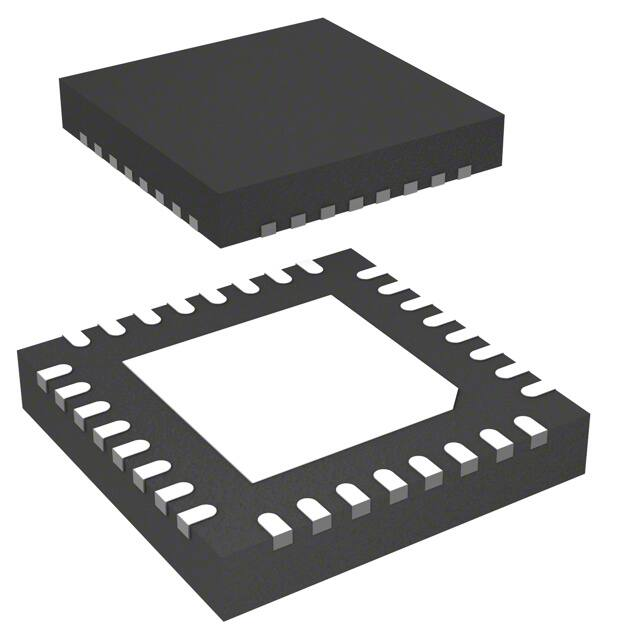


 工商网监
湘ICP备2023018690号
工商网监
湘ICP备2023018690号
