Product
Folder
Order
Now
Support &
Community
Tools &
Software
Technical
Documents
DRV10983-Q1
SLVSD14A – JUNE 2017 – REVISED JUNE 2020
DRV10983-Q1 Automotive, Three-Phase, Sensorless BLDC Motor Driver
1 Features
•
•
1
•
•
•
•
•
•
•
•
•
•
•
•
•
•
Qualified for automotive applications
AEC-Q100 qualified with the following results:
– Device temperature grade 1: –40°C to 125°C
ambient operating temperature range
– Device HBM ESD classification level 1C
– Device CDM ESD classification level C4A
Operation voltage range:
– Motor operation, 6.2 V to 28 V
– Register setting preserved, 4.5 V to 45 V
Supports load dump voltage up to 45 V
Total driver H + L rDS(on)
– 250 mΩ at TA = 25°C
– 325 mΩ at TA = 125°C
Drive current: 2-A continuous winding current (3-A
Peak)
Configurable output PWM slew rate and frequency
for EMI management
Sensorless proprietary Back Electromotive Force
(BEMF) control scheme (no need of hall sensors)
Continuous sinusoidal 180° commutation
Initial position-detect algorithm to avoid back spin
during start-up
No external sense resistor required
Flexible user interface options:
– I2C interface: access registers for command
and feedback
– Dedicated SPEED pin: accepts either analog
or PWM input
– Dedicated FG pin: provides TACH feedback
– Spin-up profile can be customized with
EEPROM
– Forward-reverse control with DIR pin
Integrated buck converter to efficiently provide 5‑V
and 3.3-V LDOs for internal and external circuits
Supply current 8.5 mA with standby version
(DRV10983SQ)
Supply current of 48 μA with sleep version
(DRV10983Q)
Protection features
– Overcurrent protection (protection for phase-tophase, phase-to-GND and phase-to-vCC shorts
– Lock detection
– Anti-Voltage Surge (AVS) protection
– UVLO protection
•
– Thermal shutdown protection
Thermally enhanced package
2 Applications
•
•
•
•
Small automotive pumps and fans
Seat ventilation fans
Motorcycle fuel pumps
HEV battery cooling fans
3 Description
The DRV10983-Q1 device is a 3-phase sensorless
motor driver with integrated power MOSFETs, which
can provide continuous drive current up to 2 A. The
device is specifically designed for cost-sensitive, lownoise, low-external-component-count fan and pump
applications.
The DRV10983-Q1 device preserves register setting
down to 4.5 V and delivers current to the motor with
supply voltage as low as 6.2 V. If the power supply
voltage is higher than 28 V, the device stops driving
the motor and protects the DRV10983-Q1 circuitry.
This function is able to handle a load dump condition
up to 45 V.
TI provides DRV10983-Q1 tuning Guide for quick
setup and tuning of the device for optimal
performance.
Device Options:
• DRV10983Q: Sleep Version
• DRV10983SQ: Standby Version
Device Information
PART NUMBER
DRV10983-Q1
(1)
PACKAGE
BODY SIZE (NOM)
HTSSOP (24)
7.80 mm × 6.40 mm
(1) For all available packages, see the orderable addendum at
the end of the data sheet.
Application Schematic
VCC
0.1 µF
10 nF
10 µF
5V
47 µH
1 µF
1 µF
4.75 kW
4.75 kW
1
VCP
VCC 24
2
CPP
VCC 23
3
CPN
W 22
4
SW
W
5
SWGND
V 20
21
6
VREG
V 19
7
V1P8
U 18
8
GND
U 17
9
V3P3
PGND 16
10 SCL
11 SDA
12 FG
10 µF
M
PGND 15
DIR 14
SPEED 13
Interface to
Microcontroller
Copyright © 2017, Texas Instruments Incorporated
1
An IMPORTANT NOTICE at the end of this data sheet addresses availability, warranty, changes, use in safety-critical applications,
intellectual property matters and other important disclaimers. PRODUCTION DATA.
�DRV10983-Q1
SLVSD14A – JUNE 2017 – REVISED JUNE 2020
www.ti.com
Table of Contents
1
2
3
4
5
6
7
Features ..................................................................
Applications ...........................................................
Description .............................................................
Revision History.....................................................
Description (Continued) ........................................
Pin Configuration and Functions .........................
Specifications.........................................................
7.1
7.2
7.3
7.4
7.5
7.6
8
1
1
1
2
3
3
5
Absolute Maximum Ratings ...................................... 5
ESD Ratings.............................................................. 5
Recommended Operating Conditions....................... 6
Thermal Information .................................................. 6
Electrical Characteristics........................................... 7
Typical Characteristics ............................................ 12
Detailed Description ............................................ 13
8.1 Overview ................................................................. 13
8.2 Functional Block Diagram ....................................... 14
8.3 Feature Description................................................. 14
8.4 Device Functional Modes........................................ 21
8.5 Register Maps ......................................................... 47
9
Application and Implementation ........................ 64
9.1 Application Information............................................ 64
9.2 Typical Application ................................................. 64
10 Power Supply Recommendations ..................... 67
11 Layout................................................................... 67
11.1 Layout Guidelines ................................................. 67
11.2 Layout Example .................................................... 67
12 Device and Documentation Support ................. 68
12.1
12.2
12.3
12.4
12.5
Trademarks ...........................................................
Electrostatic Discharge Caution ............................
Receiving Notification of Documentation Updates
Community Resources..........................................
Glossary ................................................................
68
68
68
68
68
13 Mechanical, Packaging, and Orderable
Information ........................................................... 68
4 Revision History
Changes from Original (June 2017) to Revision A
Page
•
Updated timing information for entering and exiting sleep mode and standby mode ............................................................ 8
•
Added Analog and PWM mode timing diagrams.................................................................................................................. 10
•
Updated naming convention in Step-Down Regulator subsection ....................................................................................... 14
•
Changed the Conditions to Enter or Exit Sleep or Standby Condition table to reflect Electrical Characteristics
parameter names.................................................................................................................................................................. 18
•
Added Speed pin note to Table 1 ........................................................................................................................................ 19
•
Added subsection, Required Sequence to Enter Sleep Mode ............................................................................................. 19
•
Changed Figure 13 and Figure 14 ....................................................................................................................................... 21
•
Changed Table 4 ................................................................................................................................................................. 24
•
Updated Inductive AVS Function subsection ....................................................................................................................... 41
•
Changed eeWRnEn field description to properly reflect actual function .............................................................................. 55
•
Changed BEMF comparator hysteresis to reflect Electrical Characteristics specifications ................................................. 58
•
Changed Table 36 ............................................................................................................................................................... 65
•
Added EEprom note to Layout Guidelines ........................................................................................................................... 67
2
Submit Documentation Feedback
Copyright © 2017–2020, Texas Instruments Incorporated
Product Folder Links: DRV10983-Q1
�DRV10983-Q1
www.ti.com
SLVSD14A – JUNE 2017 – REVISED JUNE 2020
5 Description (Continued)
The DRV10983-Q1 device uses a proprietary sensorless control scheme to provide continuous sinusoidal drive,
which significantly reduces the pure tone acoustics that typically occur as a result of commutation. The interface
to the device is designed to be simple and flexible. The motor can be controlled directly through PWM, analog, or
I2C inputs. Motor speed feedback is available through both the FG pin and the I2C interface simultaneously.
The DRV10983-Q1 device features an integrated buck regulator to step down the supply voltage efficiently to 5 V
for powering both internal and external circuits. The 3.3-V LDO also may be used to provide power for external
circuits. The device is available in either a sleep mode or a standby mode version to conserve power when the
motor is not running. The standby mode (8.5 mA) version (DRV10983SQ) leaves the regulator running and the
sleep mode (48 μA) version (DRV10983Q) shuts the regulator off. Use the standby mode version in applications
where the regulator is used to power an external microcontroller. Throughout this data sheet, the DRV10983-Q1
part number is used for both devices for example DRV10983Q (sleep version) and DRV10983SQ (standby
version), except for specific discussions of sleep vs standby functionality.
An I2C interface allows the user to reprogram specific motor parameters in registers and to program the
EEPROM to help optimize the performance for a given application. The DRV10983-Q1 device is available in a
thermally-efficient HTSSOP, 24-pin package with an exposed thermal pad. The operating ambient temperature is
specified from –40°C to 125°C.
6 Pin Configuration and Functions
PWP PowerPAD™ Package
24-Pin HTSSOP With Exposed Thermal Pad
Top View
VCP
1
24
VCC
CPP
2
23
VCC
CPN
3
22
W
SW
4
21
W
SWGND
5
20
V
VREG
6
19
V
18
U
Thermal
V1P8
7
GND
8
17
U
V3P3
9
16
PGND
SCL
10
15
PGND
SDA
11
14
DIR
FG
12
13
SPEED
Pad
Not to scale
Submit Documentation Feedback
Copyright © 2017–2020, Texas Instruments Incorporated
Product Folder Links: DRV10983-Q1
3
�DRV10983-Q1
SLVSD14A – JUNE 2017 – REVISED JUNE 2020
www.ti.com
Pin Functions
PIN
N/AME
TYPE
HTSSOP
DESCRIPTION
(1)
CPN
3
P
Charge pump pin 1, use a ceramic capacitor between CPN and CPP
CPP
2
P
Charge pump pin 2, use a ceramic capacitor between CPN and CPP
DIR
14
I
Direction;
When low, phase driving sequence is U → V → W
When high, phase driving sequence is U → W → V
FG
12
O
FG signal output indicates speed of motor
GND
8
P
Digital and analog ground
15, 16
P
Power ground
SCL
10
I
I2C clock signal
SDA
11
I/O
I2C data signal
SPEED
13
I
Speed control signal for PWM or analog input speed command
SW
4
O
Step-down regulator switching node output
SWGND
5
P
Step-down regulator ground
U
17, 18
O
Motor U phase
V
19, 20
O
Motor V phase
V1P8
7
P
Internal 1.8-V digital core voltage. V1P8 capacitor must connect to GND. This is an output, but is not
specified to drive external loads.
V3P3
9
P
Internal 3.3-V supply voltage. V3P3 capacitor must connect to GND. This is an output and may drive
external loads not to exceed IV3P3_MAX.
VCC
23, 24
P
Device power supply
VCP
1
P
Charge pump output, use a ceramic capacitor between VCP and VCC
PGND
VREG
W
Thermal pad
(GND)
(1)
4
6
P
Step-down regulator output and feedback point
21, 22
O
Motor W phase
—
P
The exposed thermal pad must be electrically connected to the ground plane by soldering to the PCB
for proper operation, and connected to the bottom side of the PCB through vias for better thermal
spreading.
I = Input, O = Output, I/O = Input/output, NC = No connect, P = Power
Submit Documentation Feedback
Copyright © 2017–2020, Texas Instruments Incorporated
Product Folder Links: DRV10983-Q1
�DRV10983-Q1
www.ti.com
SLVSD14A – JUNE 2017 – REVISED JUNE 2020
7 Specifications
7.1 Absolute Maximum Ratings
over operating ambient temperature range
Input voltage (2)
(1)
MIN
MAX
VCC
–0.3
28
VCC during load dump (VCC slew rate < 1 V/µs)
–0.3
45
SPEED
–0.3
4
PGND, SWGND
–0.3
0.3
SCL, SDA
–0.3
4
DIR
–0.3
4
–1
30
U, V, W
SW
Output voltage
(2)
–1
30
VREG
–0.3
7
FG
–0.3
4
VCP
–0.3
VCC + 6
CPN
–0.3
30
CPP
–0.3
VCC + 6
V3P3
–0.3
4
UNIT
V
V
V1P8
–0.3
2.5
TJ_MAX
Maximum junction temperature
–40
150
°C
Tstg
Storage temperature
–55
150
°C
(1)
(2)
Stresses beyond those listed under Absolute Maximum Ratings may cause permanent damage to the device. These are stress ratings
only, which do not imply functional operation of the device at these or any other conditions beyond those indicated under Recommended
Operating Conditions. Exposure to absolute-maximum-rated conditions for extended periods may affect device reliability.
All voltage values are with respect to the ground terminal (GND) unless otherwise noted.
7.2 ESD Ratings
VALUE
V(ESD)
(1)
Electrostatic
discharge
Human body model (HBM), per AEC Q100-002, all pins
(1)
Charged device model (CDM), per AEC Q100-011, all pins
±2000
±750
UNIT
V
AEC Q100-002 indicates that HBM stressing shall be in accordance with the ANSI/ESDA/JEDEC JS-001 specification.
Submit Documentation Feedback
Copyright © 2017–2020, Texas Instruments Incorporated
Product Folder Links: DRV10983-Q1
5
�DRV10983-Q1
SLVSD14A – JUNE 2017 – REVISED JUNE 2020
www.ti.com
7.3 Recommended Operating Conditions
Supply voltage
Voltage range
MIN
NOM
MAX
VCC, register contents preserved
4.5
12
45
VCC, motor operational
6.2
12
28
U, V, W
–0.7
SCL, SDA, FG, SPEED, DIR
–0.1
PGND, GND, SWGND
–0.1
0.1
VCP, CPP
–0.1
VCC + 5
CPN
–0.1
VCC
SW
–0.7
VCC
TA
3.3
3.6
V
100
Step-down regulator output current (resistive mode)
5
V3P3 LDO output current (no load on VREG and V3P3 in
resitive mode)
5
Operating ambient temperature
V
29
Step-down regulator output current (buck mode)
Current range
UNIT
–40
125
mA
°C
7.4 Thermal Information
DRV10983Q
THERMAL METRIC
(1)
PWP (HTSSOP)
UNIT
24 PINS
RθJA
Junction-to-ambient thermal resistance
36.1
°C/W
RθJC(top)
Junction-to-case (top) thermal resistance
17.4
°C/W
RθJB
Junction-to-board thermal resistance
14.8
°C/W
ψJT
Junction-to-top characterization parameter
0.4
°C/W
ψJB
Junction-to-board characterization parameter
14.5
°C/W
RθJC(bot)
Junction-to-case (bottom) thermal resistance
1.1
°C/W
(1)
6
For more information about traditional and new thermal metrics, see the Semiconductor and IC Package Thermal Metrics application
report.
Submit Documentation Feedback
Copyright © 2017–2020, Texas Instruments Incorporated
Product Folder Links: DRV10983-Q1
�DRV10983-Q1
www.ti.com
SLVSD14A – JUNE 2017 – REVISED JUNE 2020
7.5 Electrical Characteristics
over operating voltage and ambient temperature range (unless otherwise noted)
PARAMETER
TEST CONDITIONS
MIN
TYP
MAX
48
54
UNIT
SUPPLY CURRENT (DRV10983Q)
IVccSLEEP1
IVcc
Sleep current
Active current
VSPEED = 0 V; VCC = 12 V; TA =
25℃
VSPEED = 0 V; VCC = 12 V; across
temperature
81
VSPEED > 0 V; buck regulator with
inductor; no motor load
10
15
VSPEED > 0 V; buck regulator with
resistor; no motor load
13
16
VSPEED = 0 V; buck regulator with
inductor
8.5
14
VSPEED = 0 V; buck regulator with
resistor
11
15
VSPEED > 0 V; buck regulator with
inductor; no motor load
10
15
VSPEED > 0 V; buck regulator with
resistor; no motor load
13
16
µA
mA
SUPPLY CURRENT (DRV10983SQ)
IVccSTBY
IVcc
Standby current
Active current
mA
mA
UVLO
VUVLO_R
UVLO rising threshold
voltage
5.8
6
6.2
V
VUVLO_F
UVLO falling threshold
voltage
5.6
5.8
6
V
VUVLO_HYS
UVLO threshold voltage
hysteresis
170
195
220
mV
VV1P8_UVLO_R
V1P8 UVLO rising threshold
1.5
1.6
1.7
V
VV1P8_UVLO_F
V1P8 UVLO falling threshold
1.4
1.55
1.65
V
VV3P3_UVLO_R
V3P3 UVLO rising threshold
2.7
2.85
2.95
V
VV3P3_UVLO_F
V3P3 UVLO falling threshold
2.5
2.7
2.8
V
VVREG_UVLO_R
VREG UVLO rising threshold
4
4.2
4.3
V
VVREG_UVLO_F
VREG UVLO falling
threshold
3.9
4.2
V
LDO OUTPUT
V3P3
Output voltage
Buck regulator with inductor, 20-mA
load
3.1
3.3
3.5
V
20
mA
Buck regulator with resistor, no load
IV3P3_MAX
Maximum load from V3P3
Only with inductor mode of buck
operation, with resistor mode no
load
V1P8
Output voltage
No load
1.7
1.8
1.9
V
4.5
5
5.5
V
100
mA
5
mA
STEP-DOWN REGULATOR
LSW = 47 µH, CSW = 10 µF
Iload = 100 mA
VREG
Regulator output voltage
IREG_MAX_L
Maximum load from VREG in
switching mode
LSW = 47 µH, CSW = 10 µF
IREG_MAX_R
Maximum load from VREG in
linear mode
RSW = 39 Ω, CSW = 10 µF
RSW = 39 Ω, CSW = 10 µF
Iload = 5 mA
Submit Documentation Feedback
Copyright © 2017–2020, Texas Instruments Incorporated
Product Folder Links: DRV10983-Q1
7
�DRV10983-Q1
SLVSD14A – JUNE 2017 – REVISED JUNE 2020
www.ti.com
Electrical Characteristics (continued)
over operating voltage and ambient temperature range (unless otherwise noted)
PARAMETER
TEST CONDITIONS
MIN
TYP
MAX
TA = 25˚C; V(VCC) > 6.5 V; Io = 1 A
250
400
TA = 125˚C; V(VCC) > 6.5V; Io = 1 A
325
550
UNIT
INTEGRATED MOSFET
rDS(ON)
Series resistance (H + L)
mΩ
SPEED – ANALOG MODE
VAN/A_FS
Analog full-speed voltage
VAN/A_ZS
Analog zero-speed voltage
V(V3P3) × 0.9
V(V3P3)
0
100
V
tSAM
Sampling period for analog
voltage on SPEED pin
320
µs
VAN/A_RES
Analog voltage resolution
6.5
mV
mV
SPEED – PWM DIGITAL MODE
VDIG_IH
PWM input high voltage
VDIG_IL
PWM input low voltage
ƒPWM
PWM input frequency
2.2
V
0.1
0.6
V
100
kHz
100
mV
STANDBY MODE (DRV10983SQ)
VEN_SB
Analog voltage to enter
standby mode
SpdCtrlMd = 0 (analog mode)
VEX_SB
Analog voltage to exit
standby mode
SpdCtrlMd = 0 (analog mode)
0.17
tEX_SB_ANA
Time needed to exit from
standby mode
SpdCtrlMd = 0 (analog mode)
VSPEED > VEX_SB
1
tEX_SB_DR_ANA
Time taken to drive motor
after exiting standby mode
SpdCtrlMd = 0 (analog mode)
VSPEED > VEX_SB; ISDen = 0;
BrkDoneThr[2:0] = 0
tEX_SB_PWM
Time needed to exit from
standby mode
tEX_SB_DR_PWM
V
700
ms
350
ms
SpdCtrlMd = 1 (PWM mode)
VSPEED > VDIG_IH
2
µs
Time taken to drive motor
after exiting standby mode
SpdCtrlMd = 1 (PWM mode)
VSPEED_DUTY > 0; ISDen = 0;
BrkDoneThr[2:0] = 0
350
ms
tEN_SB_ANA
Time needed to enter
standby mode
SpdCtrlMd = 0 (analog mode)
VSPEED < VEN_SB; AvSIndEn = 0
6
ms
tEN_SB_PWM
Time needed to enter
standby mode
SpdCtrlMd = 1 (PMW mode)
VSPEED < VDIG_IL; AvSIndEn = 0
60
ms
8
Submit Documentation Feedback
Copyright © 2017–2020, Texas Instruments Incorporated
Product Folder Links: DRV10983-Q1
�DRV10983-Q1
www.ti.com
SLVSD14A – JUNE 2017 – REVISED JUNE 2020
Electrical Characteristics (continued)
over operating voltage and ambient temperature range (unless otherwise noted)
PARAMETER
TEST CONDITIONS
MIN
TYP
MAX
UNIT
100
mV
SLEEP MODE (DRV10983Q)
VEN_SL
Analog voltage to enter sleep
SpdCtrlMd = 0 (analog mode)
mode
VEX_SL
Analog voltage to exit sleep
mode
SpdCtrlMd = 0 (analog mode)
tEX_SL_ANA
Time needed to exit from
sleep mode
SpdCtrlMd = 0 (analog mode)
VSPEED > VEX_SL
2
µs
tEX_SL_DR_ANA
SpdCtrlMd = 0 (analog mode)
Time taken to drive motor
after exiting from sleep mode VSPEED > VEX_SL; ISDen = 0;
BrkDoneThr[2:0] = 0
350
ms
tEX_SL_PWM
Time needed to exit from
sleep mode
SpdCtrlMd = 1 (PWM mode)
VSPEED > VDIG_IH
2
µs
tEX_SL_DR_PWM
SpdCtrlMd = 1 (PWM mode)
Time taken to drive motor
after exiting from sleep mode VSPEED > VDIG_IH; ISDen = 0;
BrkDoneThr[2:0] = 0
350
ms
tEN_SL_ANA
Time needed to enter sleep
mode
SpdCtrlMd = 0 (analog mode)
VSPEED < VEN_SL; AvSIndEn = 0
6
ms
tEN_SL_PWM
Time needed to enter sleep
mode
SpdCtrlMd = 1 (PMW mode)
VSPEED < VDIG_IL; AvSIndEn = 0
60
ms
RPD_SPEED_SL
Internal SPEED pin pull
down resistance to ground
VSPEED = 0 (Sleep mode)
2.2
V
55
kΩ
2.2
V
DIGITAL I/O (DIR INPUT, FG OUTPUT )
VDIR_H
Input high
VDIR_L
Input low
VFG_OH
Output high voltage Io = 5
mA
VFG_OL
Output low voltage Io = 5 mA
0.6
3.3
V
V
0.6
V
2
I C SERIAL INTERFACE
VI2C_H
Input high
VI2C_L
Input low
fI2C
2.2
2
I C clock frequency
V
0
0.6
V
400
kHz
LOCK DETECTION RELEASE TIME
tLOCK_OFF
Lock release time
tLCK_ETR
Lock enter time
5
s
0.3
s
OVERCURRENT PROTECTION
IOC_limit_HS
HS overcurrent protection
VCC < 28.5 V
3.5
4.25
5.5
A
IOC_limit_LS
LS overcurrent protection
VCC < 28.5 V
3.5
4.25
5.5
A
THERMAL SHUTDOWN
TSDN
Junction temperature
shutdown threshold
150
165
180
°C
TSDN_HYS
Junction temperature
shutdown hysteresis
15
20
25
°C
TWARN
Junction temperature
warning threshold
115
125
140
°C
Submit Documentation Feedback
Copyright © 2017–2020, Texas Instruments Incorporated
Product Folder Links: DRV10983-Q1
9
�DRV10983-Q1
SLVSD14A – JUNE 2017 – REVISED JUNE 2020
www.ti.com
Electrical Characteristics (continued)
over operating voltage and ambient temperature range (unless otherwise noted)
PARAMETER
TEST CONDITIONS
MIN
TYP
MAX
UNIT
PHASE DRIVER
SLPH_LH0
Phase slew rate switching
low to high
PHslew = 0; measure 20% to 80%;
VCC = 12 V
85
120
145
V/µs
SLPH_LH1
Phase slew rate switching
low to high
PHslew = 1; measure 20% to 80%;
VCC = 12 V
60
80
100
V/µs
SLPH_LH2
Phase slew rate switching
low to high
PHslew = 2; measure 20% to 80%;
VCC = 12 V
38
50
62
V/µs
SLPH_LH3
Phase slew rate switching
low to high
PHslew = 3; measure 20% to 80%;
VCC = 12 V
27
35
44
V/µs
SLPH_HL0
Phase slew rate switching
high to low
PHslew = 0; measure 80% to 20%;
VCC = 12 V
85
120
145
V/µs
SLPH_HL1
Phase slew rate switching
high to low
PHslew = 1; measure 80% to 20%;
VCC = 12 V
59
80
100
V/µs
SLPH_HL2
Phase slew rate switching
high to low
PHslew = 2; measure 80% to 20%;
VCC = 12 V
36
50
60
V/µs
SLPH_HL3
Phase slew rate switching
high to low
PHslew = 3; measure 80% to 20%;
VCC = 12 V
25
35
45
V/µs
BEMF_HYS = 0
7
20
30
BEMF_HYS = 1
17
40
51
BEMF
COMPARATOR
BEMFHYS
BEMF comparator hysteresis
mV
LOAD DUMP PROTECTION
VOV_R
Load dump protection mode
entry on rising VCC threshold
28.5
29.2
30
V
VOV_F
Load dump protection mode
exit on falling VCC threshold
27.7
28.2
28.8
V
VOV_HYS
Load dump protection mode
hysteresis
0.73
1
1.1
V
Speed Pin VEX_SL
VEN_SL
tEX_SL_ANA
tEN_SL_ANA
V1P8
tEX_SL_DR_ANA
Phase Pin
Motor Drive State
Figure 1. DRV10983Q Analog Mode Timing
10
Submit Documentation Feedback
Copyright © 2017–2020, Texas Instruments Incorporated
Product Folder Links: DRV10983-Q1
�DRV10983-Q1
www.ti.com
SLVSD14A – JUNE 2017 – REVISED JUNE 2020
VDIG_IH
Speed Pin
VDIG_IL
tEX_SL_PWM
tEN_SL_PWM
V1P8
tEX_SL_DR_PWM
Phase Pin
Motor Drive State
Figure 2. DRV10983Q PWM Mode Timing
Speed Pin VEX_SB
VEN_SB
tEX_SB_ANA
tEN_SB_ANA
Internal
Signal
(Digital
Reset)
tEX_SB_DR_ANA
Phase Pin
Motor Drive State
Figure 3. DRV10983SQ Analog Mode Timing
VDIG_IH
Speed Pin
VDIG_IL
tEX_SB_PWM
tEN_SB_PWM
Internal
Signal
(Digital
Reset)
tEX_SB_DR_PWM
Phase Pin
Motor Drive State
Figure 4. DRV10983SQ PWM Mode Timing
Submit Documentation Feedback
Copyright © 2017–2020, Texas Instruments Incorporated
Product Folder Links: DRV10983-Q1
11
�DRV10983-Q1
SLVSD14A – JUNE 2017 – REVISED JUNE 2020
www.ti.com
7.6 Typical Characteristics
5.2
IVCC
Switching Regulator Output (V)
Supply Current, Standby Mode (mA)
15
12
9
6
3
0
5
4.9
4.8
0
5
10
15
20
Power Supply (V)
25
30
0
D001
Figure 5. Supply Current vs Power Supply Voltage
12
5.1
5
10
15
20
Power Supply (V)
25
30
D002
Figure 6. Step-Down Regulator Output vs Power Supply
Voltage
Submit Documentation Feedback
Copyright © 2017–2020, Texas Instruments Incorporated
Product Folder Links: DRV10983-Q1
�DRV10983-Q1
www.ti.com
SLVSD14A – JUNE 2017 – REVISED JUNE 2020
8 Detailed Description
8.1 Overview
The DRV10983-Q1 device is a three-phase sensorless motor driver with integrated power MOSFETs that
provides drive-current capability up to 2 A continuously. The device is specifically designed for low-noise, lowexternal-component-count motor-drive applications. The device is configurable through a simple I2C interface to
accommodate different motor parameters and spin-up profiles for different customer applications.
A 180° sensorless control scheme provides continuous sinusoidal output voltages to the motor phases to enable
ultra-quiet motor operation by keeping the electrically induced torque ripple small.
The DRV10983-Q1 device features extensive protection and fault-detection mechanisms to ensure reliable
operation. Voltage surge protection prevents the input VCC capacitor from overcharging, which is typical during
motor deceleration. The device provides overcurrent protection without the need for an external current-sense
resistor. Rotor-lock detection is available through several methods. These methods can be configured with
register settings to ensure reliable operation. The device provides additional protection for undervoltage lockout
(UVLO) and for thermal shutdown.
The commutation control algorithm continuously measures the motor phase current and periodically measures
the VCC supply voltage. The device uses this information for BEMF estimation, and the information is also
provided through the I2C register interface for debug and diagnostic use in the system, if desired.
A buck step-down regulator efficiently steps down the supply voltage. The output of this regulator provides power
for the internal circuits and can also be used to provide power for an external circuit such as a microcontroller. If
providing power for an external circuit is not necessary (and to reduce system cost), configure the buck stepdown regulator as a linear regulator by replacing the inductor with a resistor.
The DRV10983-Q1 device has a flexible interface, capable of supporting both analog and digital inputs. In
addition to the I2C interface, the device has FG, DIR, and SPEED pins. SPEED is the speed command input pin.
DIR is the direction control input pin. FG is the speed indicator output, which shows the frequency of the motor
commutation.
EEPROM is integrated in the DRV10983-Q1 device as memory for the motor parameter and operation settings.
EEPROM data transfers to the registers after power-on and exit from sleep mode.
The DRV10983-Q1 device can also operate in register mode. If the system includes a microcontroller
communicating through the I2C interface, the device can dynamically update the motor parameters and operation
settings by writing to the registers. In this configuration, the EEPROM data is bypassed by the register settings.
Submit Documentation Feedback
Copyright © 2017–2020, Texas Instruments Incorporated
Product Folder Links: DRV10983-Q1
13
�DRV10983-Q1
SLVSD14A – JUNE 2017 – REVISED JUNE 2020
www.ti.com
8.2 Functional Block Diagram
SDA
I2C
Communication
SCL
Register
EEPROM
VCC
SW
VREG
VCP
Charge
Pump
5-V Step-Down
Regulator
CPP
SWGND
CPN
V3P3
3.3-V LDO
V1P8
FG
VCC
1.8-V LDO
GND
VCP
Oscillator
Band Gap
U
V
W
V/I
Sensor
U
PreDriver
ADC
Logic
Core
VCC
VCP
SPEED
PWM and Analog
Speed Control
V
PreDriver
DIR
Lock
VCC
Overcurrent
VCP
Thermal
UVLO
GND
PreDriver
W
PGND
Copyright © 2017, Texas Instruments Incorporated
8.3 Feature Description
8.3.1 Regulators
8.3.1.1 Step-Down Regulator
The DRV10983-Q1 device includes a step-down hysteretic voltage regulator that can be operated as either a
switching buck regulator using an external inductor or as a linear regulator using an external resistor. The best
efficiency is achieved when the step-down regulator is in buck mode (see Figure 7). The regulator output voltage
is 5 V. When the regulated voltage drops by the hysteresis level, the high-side FET turns on to raise the
regulated voltage back to the target of 5 V. The switching frequency of the hysteretic regulator is not constant
and changes with load.
If the step-down regulator is configured in buck mode, see IREG_MAX_L in Electrical Characteristics to determine
the amount of current provided for external load. If the step-down regulator is configured in linear mode, see
IREG_MAX_R in Electrical Characteristics to determine the amount of current provided for external load. Active
current ICC is higher in buck mode compared to linear mode.
14
Submit Documentation Feedback
Copyright © 2017–2020, Texas Instruments Incorporated
Product Folder Links: DRV10983-Q1
�DRV10983-Q1
www.ti.com
SLVSD14A – JUNE 2017 – REVISED JUNE 2020
Feature Description (continued)
IC
IC
VCC
VREG
VCC
VREG
47 µH
5V
39 Ω
SW
10 µF
Load
SW
5V
10 µF
SWGND
SWGND
Buck Regulator with External Inductor
Buck Regulator with External Resistor
Figure 7. Step-Down Regulator Configurations
8.3.1.2 3.3-V and 1.8-V LDO
The DRV10983-Q1 device includes a 3.3-V LDO and a 1.8-V LDO. The 3.3-V LDO is powered by Vreg and 1.8V LDO is powered by 3.3-V LDO. The 1.8-V LDO is for internal circuits only. The 3.3-V LDO is mainly for internal
circuits, but can also drive external loads not to exceed IV3P3_MAX. For example, it can work as a pullup voltage
for the FG, DIR, SDA, and SCL interface.
Both the V1P8 and V3P3 capacitors must be connected to GND.
8.3.2 Protection Circuits
8.3.2.1 Thermal Shutdown
The DRV10983-Q1 device has a built-in thermal shutdown function, which shuts down the device when the
junction temperature is more than TSDN˚C and recovers operating conditions when the junction temperature falls
to TSDN – TSDN_HYS˚C.
The OverTemp status bit (address 0x00, bit 15) is set during thermal shutdown. In addition to the thermal
shutdown function there is a warning bit that is set whenever the device exceeds TWARN and is indicated by the
TempWarning bit of the FaultReg register (address 0x00, bit 14).
8.3.2.2 Undervoltage Lockout (UVLO)
The DRV10983-Q1 device has a built-in UVLO function block. The device is locked out when VCC is below
VUVLO_F and is unlocked when VCC is above VUVLO_R. The hysteresis of the UVLO threshold is VUVLO_HYS. In
addition to the main supply, the step-down regulator, charge pump, and 3.3-V LDO all have undervoltage lockout
monitors.
8.3.2.3 Overcurrent Protection
The overcurrent protection function acts to protect the device if the current, as measured from the FETs, exceeds
the IOC-limit threshold. It protects the device in the event of a short-circuit condition on the motor phases. This
includes phase shorts to GND, phase shorts to phase, or phase shorts to VCC. The DRV10983-Q1 device places
the output drivers into a high-impedance state until the lock time tLOCK_OFF has expired. The OverCurr status bit
of the FaultReg register (address 0x00, bit 11) is set.
The DRV10983-Q1 device also provides acceleration current-limit and lock-detection current-limit functions to
protect the device and motor (see Current Limit and Lock Detect and Fault Handling ).
Submit Documentation Feedback
Copyright © 2017–2020, Texas Instruments Incorporated
Product Folder Links: DRV10983-Q1
15
�DRV10983-Q1
SLVSD14A – JUNE 2017 – REVISED JUNE 2020
www.ti.com
Feature Description (continued)
8.3.2.4 Lock
When the motor is blocked or stopped by an external force, lock protection is triggered, and the device stops
driving the motor immediately. After the lock release time tLOCK_OFF, the DRV10983-Q1 device resumes driving
the motor again. If the lock condition is still present, it enters the next lock protection cycle, and repeats until the
lock condition is removed. With this lock protection, the motor and device do not overheat or become damaged
due to the motor being locked (see Lock Detect and Fault Handling ).
During a lock condition the Status register indicates which of the locks has occurred.
8.3.3 Motor Speed Control
The DRV10983-Q1 device offers four methods for indirectly controlling the speed of the motor by adjusting the
output voltage amplitude. This can be accomplished by varying the supply voltage (VCC) or by controlling the
speed command. The speed command can be controlled in one of three ways. The user can set the speed
command by adjusting either the PWM input (PWM in) or the analog input (Analog) or by writing the speed
command directly through the I2C serial port (I2C). The speed command is used to determine the PWM duty
cycle output (PWM_DCO) (see Figure 9).
The input PWM input (PWM in) can have a minimum duty cycle limit applied. DutyCycleLimit[1:0], accessible
through the I2C interface, allows the user to configure the minimum duty cycle behavior. This behavior is
illustrated in Figure 8.
DutyCycleLimit[1:0], Reg0x95
00 - linear down to 5%, then holds at 5% until
duty command is 1.5 %; 0 % for duty command
below 1.5 %.
01 - linear down to 10%, then holds at 10% until
duty command is 1.5 %; 0 % for duty command
below 1.5 %.
Output Duty
Cycle (%)
100
10
10
5
5
0
Input Duty Cycle
0 1.5
5
10
Input Duty Cycle (%)
DutyCycleLimit[1:0], Reg0x95
10 - linear down to 5%, then holds at 5% until
duty command is 1.5 %; 100 % for duty command
below 1.5 %.
11 - linear down to 10%, then holds at 10% until
duty command is 1.5 %; 100 % for duty command
below 1.5 %.
Output Duty
Cycle (%)
0
0 1.5
5
10
Input Duty Cycle (%)
Figure 8. Duty Cycle Profile
The speed command may not always be equal to the PWM_DCO because the DRV10983-Q1 device has the
AVS function (see Anti Voltage Suppression Function), the acceleration current-limit function (see Acceleration
Current Limit), and the closed-loop accelerate function (see Closed-Loop Accelerate) to optimize the control
performance. These functions can limit the PWM_DCO, which affects the output amplitude (see Figure 9).
16
Submit Documentation Feedback
Copyright © 2017–2020, Texas Instruments Incorporated
Product Folder Links: DRV10983-Q1
�DRV10983-Q1
www.ti.com
SLVSD14A – JUNE 2017 – REVISED JUNE 2020
Feature Description (continued)
PWM In
PWM Duty
Analog
ADC
SPEED Pin
AVS,
Acceleration Current Limit
Closed Loop Accelerate
Speed
Command
2
IC
PWM_
DCO
VCC
Output
Amplitude
X
Motor
Copyright © 2017, Texas Instruments Incorporated
Figure 9. Multiplexing the Speed Command to the Output Amplitude Applied to the Motor
The output voltage amplitude applied to the motor is developed through sine wave modulation so that the phaseto-phase voltage is sinusoidal.
When any phase is measured with respect to ground, the waveform is sinusoidally coupled with third-order
harmonics. This encoding technique permits one phase to be held at ground while the other two phases are
pulse-width modulated. Figure 10 and Figure 11 show the sinusoidal encoding technique used in the DRV10983Q1 device.
PWM Output
Average Value
Figure 10. PWM Output and the Average Value
U-V
U
V-W
V
W-U
W
Sinusoidal voltage from phase to phase
Sinusoidal voltage with third-order harmonics
from phase to GND
Figure 11. Representing Sinusoidal Voltages With Third-Order Harmonic Output
The output amplitude is determined by the magnitude of VCC and the PWM duty cycle output (PWM_DCO). The
PWM_DCO represents the peak duty cycle that is applied in one electrical cycle. The maximum amplitude is
reached when PWM_DCO is at 100%. The peak output amplitude is VCC. When the PWM_DCO is at 50%, the
peak amplitude is VCC / 2 (see Figure 12).
Submit Documentation Feedback
Copyright © 2017–2020, Texas Instruments Incorporated
Product Folder Links: DRV10983-Q1
17
�DRV10983-Q1
SLVSD14A – JUNE 2017 – REVISED JUNE 2020
www.ti.com
Feature Description (continued)
100% PWM DCO
50% PWM DC0
VCC
VCC / 2
Figure 12. Output Voltage Amplitude Adjustment
Motor speed is controlled indirectly by controlling the output amplitude, which is achieved by either controlling
VCC, or controlling the PWM_DCO. The DRV10983-Q1 device provides different options for the user to control
the PWM_DCO:
• Analog input (SPEED pin)
• PWM encoded digital input (SPEED pin)
• I2C serial interface.
See the Closed Loop section for more information.
8.3.4 Load Dump Handling
The recommended operation voltage of the DRV10983-Q1 device is from 6.2 V to 28 V. The device is able to
drive the motor within this VCC range.
In the load dump condition, VCC can rise up to 45 V. Once the DRV10983-Q1 device detects that VCC is higher
than VOV_R , it stops driving the motor and protects its own circuitry. When VCC drops below VOV_F, the
DRV10983-Q1 device continues to operate the motor based on the user’s command.
8.3.5 Sleep or Standby Condition
The DRV10983-Q1 device is available in either a sleep mode (DRV10983Q) or standby mode version
(DRV10983SQ). The DRV10983-Q1 device enters either sleep or standby to conserve energy. When the device
enters either sleep or standby, the device stops driving the motor. The step-down regulator is disabled in the
sleep mode version to conserve more energy. The I2C interface is disabled and any register data not stored in
EEPROM is reset for the sleep mode version. The step-down regulator remains active in the standby mode
version. The register data is maintained, and the I2C interface remains active for standby mode version.
For different speed command modes, shows the timing and command to enter the sleep or standby condition.
Table 1. Conditions to Enter or Exit Sleep or Standby Condition
18
SPEED COMMAND
MODE
ENTER STANDBY
CONDITION
ENTER SLEEP
CONDITION
EXIT FROM STANDBY
CONDITION
EXIT FROM SLEEP
CONDITION
Analog
SPEED pin voltage <
VEN_SB for tEN_SB_ANA
SPEED pin voltage <
VEN_SL for tEN_SL_ANA
SPEED pin voltage >
VEX_SB for tEX_ SB_ANA
SPEED pin voltage >
VEX_SL for tEX_SL_ANA
PWM
SPEED pin low (V <
VDIG_IL) for tEN_SB_PWM
SPEED pin low (V <
VDIG_IL) for tEN_SL_PWM
SPEED pin high (V >
VDIG_IH) for tEX_SB_PWM
SPEED pin high (V >
VDIG_IH) for tEX_SL_PWM
I2C
SpdCtrl[8:0] is
programmed as 0 for
tEN_SB_PWM
See Required Sequence to
Enter Sleep Mode
Changed Table 4
SpdCtrl[8:0] is programmed
as non-zero for tEX_SB_PWM
SPEED pin high (V >
VDIG_IH) for tEX_SL_PWM
(PWM mode) or SPEED
pin voltage > VEX_SL for
tEX_SL_ANA (Analog mode)
Submit Documentation Feedback
Copyright © 2017–2020, Texas Instruments Incorporated
Product Folder Links: DRV10983-Q1
�DRV10983-Q1
www.ti.com
SLVSD14A – JUNE 2017 – REVISED JUNE 2020
Speed pin in DRV10983SQ (Standby version) and DRV10983Q (sleep version) should be in known state (pulled
high or low) when the speed is controlled via I2C.
Note that when using the analog speed command, a higher voltage is required to exit from the sleep condition
than from the standby condition. The I2C speed command cannot take the device out of the sleep condition
because I2C communication is disabled during the sleep condition.
Table 2. Minimum PWM Duty Cycle Requirement for Different PWM Frequency to Exit Sleep Condition
INPUT PWM FREQUENCY (kHz)
PWM DUTY CYCLE (%)
0.1 to 0.5
14
0.5 to 1
11
1 to 50
9
50 to 100
4
100
3.5
8.3.5.1 Required Sequence to Enter Sleep Mode
In I2C speed command mode, either of two sequence options can be used to enter sleep mode.
8.3.5.1.1 Option 1
1. Provide a non-zero value to the speed control register. For example, write 100 to register 0x30,
speedCtrl[8:0].
2. Set the I2C OverRide bit to 1. That is, write 1 to register 0x30, speedCtrl[15].
3. In analog mode, be sure SPEED pin voltage is less than VEN_SL for tEN_SL_ANA. In PWM mode, make sure
SPEED pin is low (V < VDIG_IL) for tEN_SL_PWM.
4. Provide the value of zero to the speed control register to enter sleep mode. That is, write 0 to register 0x30,
speedCtrl[8:0].
8.3.5.1.2 Option 2
1.
2.
3.
4.
Set the motor disable bit to 1. That is, write 1 to register 0x60, EECtrl[15].
Set the I2C OverRide bit to 1. That is, write 1 to register 0x30, speedCtrl[15].
Set the motor disable bit to 0. That is, write 0 to register 0x60, EECtrl[15].
Provide the value of zero to the speed control register to enter sleep mode. That is, write 0 to register 0x30,
speedCtrl[8:0].
8.3.6 EEPROM Access
The DRV10983-Q1 device has 112 bits (7 registers with 16-bit width) of EEPROM data, which are used to
program the motor parameters as described in the I2C Serial Interface.
The procedure for programming the EEPROM is as follows. TI recommends to perform the EEPROM
programming without the motor spinning, cycle the power after the EEPROM write, and read back the EEPROM
to verify the programming is successful.
1. Power up with any voltage within operating voltage range (6.2 V to 28 V)
2. (DRV10983Q only) Exit from sleep condition
3. Wait 10 ms
4. Write register 0x60 to set MTR_DIS = 1; this disables the motor driver.
5. Write register 0x31 with 0x0000 to clear the EEPROM access code
6. Write register 0x31 with 0xC0DE to enable access to EEPROM
7. Read register 0x32 for eeReadyStatus = 1
8. Case-A: Mass Write
A. Write all individual shadow registers
a. Write register 0x90 (CONFIG1) with CONFIG1 data
b. ...
Submit Documentation Feedback
Copyright © 2017–2020, Texas Instruments Incorporated
Product Folder Links: DRV10983-Q1
19
�DRV10983-Q1
SLVSD14A – JUNE 2017 – REVISED JUNE 2020
www.ti.com
c. Write register 0x96 (CONFIG7) with CONFIG7 data
B. Write the following to register 0x35
a. ShadowRegEn = 0
b. eeRefresh = 0
c. eeWRnEn = 1
d. EEPROM Access Mode = 10
C. Wait for register 0x32 eeReadyStatus = 1 – EEPROM is now updated with the contents of the shadow
registers.
9. Case-B: Mass Read
A. Write the following to register 0x35
a. ShadowRegEn = 0
b. eeRefresh = 0
c. eeWRnEn = 0
d. eeAccMode = 10
B. Internally, the device starts reading the EEPROM and storing it in the shadow registers.
C. Wait for register 0x32 eeReadyStatus = 1 – shadow registers now contain the EEPROM values
10. Write register 0x60 to set MTR_DIS = 0; this re-enables the motor driver
20
Submit Documentation Feedback
Copyright © 2017–2020, Texas Instruments Incorporated
Product Folder Links: DRV10983-Q1
�DRV10983-Q1
www.ti.com
SLVSD14A – JUNE 2017 – REVISED JUNE 2020
8.4 Device Functional Modes
This section includes the logic required to be able to reliably start and drive the motor. It describes the processes
used in the logic core and provides the information needed to configure the parameters effectively to work over a
wide range of applications.
8.4.1 Motor Parameters
See the DRV10983-Q1 Tuning Guide for the motor parameter measurement.
The motor phase resistance and BEMF constants are two important parameters used to characterize a BLDC
motor. The DRV10983-Q1 device requires these parameters to be configured in the register. The motor phase
resistance is programmed by writing the values for Rm[6:0] (combination of RMShift[2:0] and RMValue[3:0]) in
the Config1 register. The BEMF constant is programmed by writing the values for Kt[6:0] (combination of
KTShift[2:0] and KTValue[3:0]) in the Config2 register.
8.4.1.1 Motor Phase Resistance
For a wye-connected motor, the motor phase resistance refers to the resistance from the phase output to the
center tap, RPH_CT (denoted as RPH_CT in Figure 13).
Phase U
RPH_CT
RPH_CT
RPH_CT
Center
Tap
Phase V
Phase W
Figure 13. Wye-Connected Motor Phase Resistance
For a delta-connected motor, the motor phase resistance refers to the equivalent phase to center tap in the wye
configuration. In Figure 14, it is denoted as RY. RPH_CT = RY.
For both the delta-connected motor and the wye-connected motor, the easy way to get the equivalent RPH_CT is
to measure the resistance between two phase terminals (RPH_PH), and then divide this value by two, RPH_CT = ½
RPH_PH.
Phase U
RY
RPH_PH
RY
Phase V
RPH_PH
Center
Tap
RPH_PH
RY
Phase W
Figure 14. Delta-Connected Motor and the Equivalent Wye Connections
Submit Documentation Feedback
Copyright © 2017–2020, Texas Instruments Incorporated
Product Folder Links: DRV10983-Q1
21
�DRV10983-Q1
SLVSD14A – JUNE 2017 – REVISED JUNE 2020
www.ti.com
Device Functional Modes (continued)
The motor phase resistance (RPH_CT) must be converted to a 7-bit digital register value Rm[6:0] to program the
motor phase resistance value. The digital register value can be determined as follows:
1. Convert the motor phase resistance (RPH_CT) to a digital value where the LSB is weighted to represent 9.67
mΩ: Rmdig = RPH_CT / 0.00967.
2. Encode the digital value such that Rmdig = RMValue[3:0]
BrkDoneThr
Y
Y
N
N
Align
Accelerate
RvsDr
IPD
N
ClosedLoop
Speed >
Op2CIsThr
Y
Figure 17. Motor Starting-Up Flow
Power-On State This is the initial power-on state of the motor start sequencer (MSS). The MSS starts in this
state on initial power-up or whenever the DRV10983-Q1 device comes out of either standby or
sleep mode.
ISDen Judgment After power-on, the DRV10983-Q1 MSS enters the ISDen judgment where it checks to see if
the initial speed detect (ISD) function is enabled (ISDen = 1). If ISD is disabled, the MSS proceeds
directly to the BrkEn Judgment. If ISD is enabled, the motor start sequence advances to the ISD
state.
ISD State
The MSS determines the initial condition of the motor (see Initial Speed Detect).
SpeedRvsDrThr.
Speed>RvsDrThr Judgment The motor start sequencer checks to see if the reverse speed is greater than the
threshold defined by RvsDrThr[1:0]. If it is, then the MSS returns to the ISD state to allow the motor
to decelerate. This prevents the DRV10983-Q1 device from attempting to reverse drive or brake a
motor that is spinning too quickly. If the reverse speed of the motor is less than the threshold
defined by RvsDrThr[1:0], then the MSS advances to the RvsDrEn judgment.
RvsDrEn Judgment The MSS checks to see if the reverse drive function is enabled (RvsDrEn = 1). If it is, the
MSS transitions into the RvsDr state. If the reverse drive function is not enabled, the MSS
advances to the BrkEn judgment.
RvsDr State The DRV10983-Q1 device drives the motor in the forward direction to force it to rapidly decelerate
(see Reverse Drive). When it reaches zero velocity, the MSS transitions to the Accelerate state.
BrkEn Judgment The MSS checks to determine whether the brake function is enabled (BrkDoneThr[2:0] ≠ 000).
If the brake function is enabled, the MSS advances to the brake state.
Brake State The device performs the brake function (see Motor Brake).
Time>BrkDoneThr Judgment The MSS applies brake for a time configured by BRKDoneThr[2:0]. After brake
state, the MSS advances to the IPDEn judgment.
IPDEn Judgment The MSS checks to see if IPD has been enabled (IPDCurrThr[3:0] ≠ 0000). If the IPD is
enabled, the MSS transitions to the IPD state. Otherwise, it transitions to the align state.
Align State The DRV10983-Q1 device performs the align function (see Align). After the align completes, the
MSS transitions to the Accelerate state.
IPD State
The DRV10983-Q1 device performs the IPD function. The IPD function is described in Initial
Position Detect (IPD). After the IPD completes, the MSS transitions to the accelerate state.
Accelerate State The DRV10983-Q1 device accelerates the motor according to the settings of StAccel and
StAccel2. After applying the accelerate settings, the MSS advances to the Speed>Op2ClsThr
judgment.
Speed>Op2ClsThr Judgment The motor accelerates until the drive rate exceeds the threshold configured by
the Op2ClsThr[4:0] settings. When this threshold is reached, the DRV10983-Q1 device enters into
the ClosedLoop state.
ClosedLoop State In this state, the DRV10983-Q1 device drives the motor based on feedback from the
commutation control algorithm.
DIR Pin Change Judgment If the DIR pin is changed during any of above states, DRV10983-Q1 device stops
driving the motor and restarts from the beginning.
8.4.3.1 Initial Speed Detect
The ISD function is used to identify the initial condition of the motor. If the function is disabled, the DRV10983-Q1
device does not perform the initial speed detect function and treats the motor as if it is stationary.
Phase-to-phase comparators are used to detect the zero crossings of the motor’s BEMF voltage while it is
coasting (motor phase outputs are in the high-impedance state). Figure 18 shows the configuration of the
comparators.
Submit Documentation Feedback
Copyright © 2017–2020, Texas Instruments Incorporated
Product Folder Links: DRV10983-Q1
27
�DRV10983-Q1
SLVSD14A – JUNE 2017 – REVISED JUNE 2020
www.ti.com
60 degrees
±
V
+
U
+
±
W
Figure 18. Initial Speed Detect Function
If the UW comparator output is lagging the UV comparator by 60°, the motor is spinning forward. If the UW
comparator output is leading the UV comparator by 60°, the motor is spinning in reverse.
The motor speed is determined by measuring the time between two rising edges of either of the comparators.
If neither of the comparator outputs toggles for a given amount of time, the condition is defined as stationary. The
amount of time can be programmed by setting the register bits ISDThr[1:0].
8.4.3.2 Motor Resynchronization
The resynchronize function works when the ISD function is enabled and determines that the initial state of the
motor is spinning in the forward direction. The speed and position information measured during ISD are used to
initialize the drive state of the DRV10983-Q1 device, which can transition directly into the closed-loop running
state without needing to stop the motor.
8.4.3.3 Reverse Drive
The ISD function measures the initial speed and the initial position; the DRV10983-Q1 reverse drive function acts
to reverse accelerate the motor through zero speed and to continue accelerating until the closed loop threshold is
reached (see Figure 19). If the reverse speed is greater than the threshold configured in RvsDrThr[1:0], then the
DRV10983-Q1 device waits until the motor coasts to a speed that is less than the threshold before driving the
motor to reverse accelerate.
Speed
Closed loop
Op2ClsThr
Open loop
Time
RevDrThr
Reverse Drive
Coasting
Figure 19. Reverse Drive Function
28
Submit Documentation Feedback
Copyright © 2017–2020, Texas Instruments Incorporated
Product Folder Links: DRV10983-Q1
�DRV10983-Q1
www.ti.com
SLVSD14A – JUNE 2017 – REVISED JUNE 2020
Reverse drive is suitable for applications where the load condition is light at low speed and relatively constant
and where the reverse speed is low (that is, a fan motor with little friction). For other load conditions, the motor
brake function provides a method for helping force a motor which is spinning in the reverse direction to stop
spinning before a normal start-up sequence.
8.4.3.4 Motor Brake
The motor brake function can be used to stop the spinning motor before attempting to start the motor. The brake
is applied by turning on all three of the low-side driver FETs.
Brake is enabled by configuring a non-zero BrkDoneThr[2:0]. Brake is applied for a time configured by
BrkDoneThr[2:0] (forward or reverse). After the motor is stopped, the motor position is unknown. To proceed with
restarting in the correct direction, the IPD or align-and-go algorithm must be implemented. The motor start
sequence is the same as it would be for a motor starting in the stationary condition.
The motor brake function can be disabled. The motor skips the brake state and attempts to spin the motor as if it
were stationary. If this happens while the motor is spinning in either direction, the start-up sequence may not be
successful.
8.4.3.5 Motor Initialization
8.4.3.5.1 Align
The DRV10983-Q1 device aligns a motor by injecting dc current through a particular phase pattern which is
current flowing into phase V, flowing out from phase W for a certain time (configured by AlignTime[2:0]). The
current magnitude is determined by OpenLCurr[1:0]. The motor should be aligned at the known position.
The time of align affects the start-up timing (see Start-Up Timing). A bigger-inertia motor requires longer align
time.
8.4.3.5.2 Initial Position Detect (IPD)
The inductive sense method is used to determine the initial position of the motor when IPD is enabled. IPD is
enabled by selecting IPDCurrThr[3:0] to any value other than 0000.
IPD can be used in applications where reverse rotation of the motor is unacceptable. Because IPD is not
required to wait for the motor to align with the commutation, it can allow for a faster motor start sequence. IPD
works well when the inductance of the motor varies as a function of position. Because it works by pulsing current
to the motor, it can generate acoustics which must be taken into account when determining the best start method
for a particular application.
8.4.3.5.2.1 IPD Operation
The IPD operates by sequentially applying voltage across two of the three motor phases according to the
following sequence: VW WV UV VU WU UW (see Figure 20). When the current reaches the threshold configured
in IPDCurrThr[3:0], the voltage across the motor is stopped. The DRV10983-Q1 device measures the time it
takes from when the voltage is applied until the current threshold is reached. The time varies as a function of the
inductance in the motor windings. The state with the shortest time represents the state with the minimum
inductance. The minimum inductance is because of the alignment of the north pole of the motor with this
particular driving state.
Submit Documentation Feedback
Copyright © 2017–2020, Texas Instruments Incorporated
Product Folder Links: DRV10983-Q1
29
�DRV10983-Q1
SLVSD14A – JUNE 2017 – REVISED JUNE 2020
www.ti.com
U
IPDclk
N
V
Clock
S
W
Drive
VW
WV
UV
VU
WU
UW
IPDCurrThr
Current
Search the Minimum Time
Permanent
Magnet Position
Saturation Position of the
Magnetic Field
Smallest
Inductance
Minimum
Time
Figure 20. IPD Function
8.4.3.5.2.2 IPD Release Mode
Two options are available for stopping the voltage applied to the motor when the current threshold is reached. If
IPDRlsMd = 0, the recirculate mode is selected. The low-side (S6) MOSFET remains on to allow the current to
recirculate between the MOSFET (S6) and body diode (S2) (see Figure 21). If IPDRlsMd = 1, the highimpedance (Hi-Z) mode is selected. Both the high-side (S1) and low-side (S6) MOSFETs are turned off and the
current flies back across the body diodes into the power supply (see Figure 22).
In the high-impedance state, the phase current has a faster settle-down time, but that could result in a surge on
VCC. Manage this with appropriate selection of either a clamp circuit or by providing sufficient capacitance
between VCC and GND. If the voltage surge cannot be contained and if it is unacceptable for the application, then
select the recirculate mode. When selecting the recirculate mode, select the IPDClk[1:0] bits to give the current in
the motor windings enough time to decay to 0.
S1
S3
S5
M
U1
S2
Driving
S1
S4
S6
S3
S5
M
U1
S2
S4
S6
Brake (Recirculate)
Figure 21. IPD Release Mode 0
30
Submit Documentation Feedback
Copyright © 2017–2020, Texas Instruments Incorporated
Product Folder Links: DRV10983-Q1
�DRV10983-Q1
www.ti.com
SLVSD14A – JUNE 2017 – REVISED JUNE 2020
S1
S3
S5
S1
M
U1
S2
S4
S3
S5
M
U1
S6
S2
Driving
S4
S6
Hi-Z (Tri-State)
Figure 22. IPD Release Mode 1
8.4.3.5.2.3 IPD Advance Angle
After the initial position is detected, the DRV10983-Q1 device begins driving the motor at an angle specified by
IPDAdvcAgl[1:0].
Advancing the drive angle anywhere from 0° to 180° results in positive torque. Advancing the drive angle by 90°
results in maximum initial torque. Applying maximum initial torque could result in uneven acceleration to the rotor.
Select the IPDAdvcAgl[1:0] to allow for smooth acceleration in the application (see Figure 23).
Motor spinning direction
U
V
N
S
W
U
N
V
U
N
V
U
N
V
U
N
S
S
S
S
W
W
W
W
Û DGYDQFH
Û advance
Û DGYDQFH
V
Û DGYDQFH
Figure 23. IPD Advance Angle
8.4.3.5.3 Motor Start
After it is determined that the motor is stationary and after completing the motor initialization with either align or
IPD, the DRV10983-Q1 device begins to accelerate the motor. This acceleration is accomplished by applying a
voltage determined by the open-loop current setting (OpenLCurr[1:0]) to the appropriate drive state and by
increasing the rate of commutation without regard to the real position of the motor (referred to as open-loop
operation). The function of the open-loop operation is to drive the motor to a minimum speed so that the motor
generates sufficient BEMF to allow the commutation control logic to accurately drive the motor.
Table 5 lists the configuration options that can be set in register to optimize the initial motor acceleration stage
for different applications.
Submit Documentation Feedback
Copyright © 2017–2020, Texas Instruments Incorporated
Product Folder Links: DRV10983-Q1
31
�DRV10983-Q1
SLVSD14A – JUNE 2017 – REVISED JUNE 2020
www.ti.com
Table 5. Configuration Options for Controlling Open-Loop Motor Start
REG. NAME
CONFIGURATION
BITS
MIN. VALUE
MAX. VALUE
Open- to closed-loop threshold
CONFIG4
Op2ClsThr[4:0]
0.8 Hz
204.8 Hz
Align time
CONFIG4
AlignTime[2:0]
40 ms
5.3 s
First-order accelerate
CONFIG4
StAccel[2:0]
0.019 Hz/s
76 Hz/s
Second-order accelerate
CONFIG4
StAccel2[2:0]
0.0026 Hz/s2
57 Hz/s2
CONFIG3
OpenLCurr[1:0]
200 mA
1.6 A
CONFIG3
OpLCurrRt[2:0]
DESCRIPTION
Open-loop current setting
Align current setting
Open-loop current ramping
150 mA
1.2 A
0.023 VCC/s
6 VCC/s
8.4.3.6 Start-Up Timing
Start-up timing is determined by the align and accelerate time. The align time can be set by AlignTime[2:0]. The
accelerate time is defined by the open-to-closed loop threshold Op2ClsThr[4:0] along with the first-order
StAccel[2:0](A1) and second-order StAccel2[2:0](A2) acceleration coefficients. Figure 24 shows the motor startup process.
Speed
Speed =
2
A1 ´ t + 0.5 A2 ´ t
Close loop
Op2ClsThr
AlignTime
Time
Accelerate Time is determined by
Op2ClsThr and A1, A2.
Accelerate Time
Figure 24. Motor Start-Up Process
Select the first-order and second-order acceleration coefficients to allow the motor to reliably accelerate from
zero velocity up to the closed-loop threshold in the shortest time possible. Using a slow acceleration coefficient
during the first order accelerate stage can help improve reliability in applications where it is difficult to accurately
initialize the motor with either align or IPD.
Select the open-to-closed loop threshold to allow the motor to accelerate to a speed that generates sufficient
BEMF for closed-loop control. This is determined by the velocity constant of the motor based on the relationship
described in Equation 2.
BEMF = KtPH × speed (Hz)
(2)
8.4.4 Align Current
During the align state, the measured align current is dependent on actual motor phase resistance and rDS(on) of
the internal FETs. The relationship between measured align current and configured align current is derived from
actual motor phase resistance, configured motor phase resistance and rDS(on).
é
ù
Rm
AlignCurrent _ Measured = AlignCurrent _ Configured ´ ê
ú
ëê R motor + rDS(on) ûú
where
•
•
•
•
•
32
AlignCurrent_Measured is the actual align current measured during the align state
AlignCurrent_Configured is the align current configured by OpenLCurr[1:0]
Rmotor is the actual motor phase resistance
rDS(on) is the resistance between the drain and source of the FETs during the on-state
Rm is configured by Rm[6:0]
Submit Documentation Feedback
(3)
Copyright © 2017–2020, Texas Instruments Incorporated
Product Folder Links: DRV10983-Q1
�DRV10983-Q1
www.ti.com
SLVSD14A – JUNE 2017 – REVISED JUNE 2020
8.4.5 Start-Up Current Setting
The start-up current setting is to control the peak start-up during open loop. During open-loop operation, it is
desirable to control the magnitude of drive current applied to the motor. This is helpful in controlling and
optimizing the rate of acceleration. The limit takes effect during reverse drive, align, and acceleration.
The start current is set by programming the OpenLCurr[1:0] bits. The current should be selected to allow the
motor to reliably accelerate to the handoff threshold. Heavier loads may require a higher current setting, but it
should be noted that the rate of acceleration is limited by the acceleration rate (StAccel[2:0], StAccel2[2:0]). If the
motor is started with more current than necessary to reliably reach the handoff threshold, it results in higher
power consumption.
The start current is controlled based on the relationship shown in Equation 4 and Figure 25. The duty cycle
applied to the motor is derived from the calculated value for ULimit and the magnitude of the supply voltage, VCC,
as well as the drive state of the motor.
ULimit ILimit u Rm Speed Hz u Kt
where
•
•
•
•
ILimit is configured by OpenLCurr[1:0]
Rm is configured by Rm[6:0]
Speed is variable based motor’s open loop acceleration profile
Kt is configured by Kt[6:0]
(4)
Rm
VU = BEMF + I × Rm
M
BEMF = Kt × speed
Copyright © 2017, Texas Instruments Incorporated
Figure 25. Motor Start-Up Current
8.4.5.1 Start-Up Current Ramp-Up
A fast change in the applied drive current may result in a sudden change in the driving torque. In some
applications, this could result in acoustic noise. To avoid this, the DRV10983-Q1 device allows the option of
limiting the rate at which the current is applied to the motor. OpLCurrRt[2:0] sets the maximum voltage ramp-up
rate that is applied to the motor. The waveforms in Figure 26 show how this feature can be used to gradually
ramp the current applied to the motor.
Start driving with fast current ramp
Start driving with slow current ramp
Figure 26. Motor Start-Up Current Ramp
8.4.6 Closed Loop
In closed loop operation, the DRV10983-Q1 device continuously samples the current in the U phase of the motor
and uses this information to estimate the BEMF voltage that is present. The drive state of the motor is controlled
based on the estimated BEMF voltage.
Submit Documentation Feedback
Copyright © 2017–2020, Texas Instruments Incorporated
Product Folder Links: DRV10983-Q1
33
�DRV10983-Q1
SLVSD14A – JUNE 2017 – REVISED JUNE 2020
www.ti.com
8.4.6.1 Half-Cycle Control and Full-Cycle Control
The estimated BEMF used to control the drive state of the motor has two zero-crosses every electrical cycle. The
DRV10983-Q1 device can be configured to update the drive state either once every electrical cycle or twice for
every electrical cycle. When AdjMode is programmed to 1, half-cycle adjustment is applied. The control logic is
triggered at both the rising edge and falling edge. When AdjMode is programmed to 0, full-cycle adjustment is
applied. The control logic is triggered only at the rising edge (see Figure 27).
Half-cycle adjustment provides a faster response when compared with full-cycle adjustment. Use half-cycle
adjustment whenever the application requires operation over large dynamic loading conditions. Use the full-cycle
adjustment for low-current ( VANA_FS, the speed command is maximum. If VANA_ZS ≤ SPEED < VANA_FS the speed command
changes linearly according to the magnitude of the voltage applied at the SPEED pin. If SPEED < VANA_ZS the
speed command is to stop the motor. Figure 28 shows the speed command when operating in analog mode.
Speed
Command
Maximum
Speed
Command
Analog Input
VANA-ZS
VANA-FS
Figure 28. Analog-Mode Speed Command
8.4.6.3 Digital PWM-Input-Mode Speed Control
If SpdCtrlMd = 1, the SPEED input pin is configured to operate as a PWM-encoded digital input. The PWM duty
cycle applied to the SPEED pin can be varied from 0 to 100%. The speed command is proportional to the PWM
input duty cycle. The speed command stops the motor when the PWM input keeps at 0 for tEN_SL_SB (see
Figure 29).
The frequency of the PWM input signal applied to the SPEED pin is defined as fPWM. This is the frequency the
device can accept to control motor speed. It does not correspond to the PWM output frequency that is applied to
the motor phase. The PWM output frequency can be configured to be either 25 kHz when the PWMFreq bit is set
to 0 or to 50 kHz when PWMFreq bit is set to 1.
34
Submit Documentation Feedback
Copyright © 2017–2020, Texas Instruments Incorporated
Product Folder Links: DRV10983-Q1
�DRV10983-Q1
www.ti.com
SLVSD14A – JUNE 2017 – REVISED JUNE 2020
Speed
Command
Maximum
Speed
Command
PWM duty
0
100%
Figure 29. PWM-Mode Speed Command
8.4.6.4 I2C-Mode Speed Control
The DRV10983-Q1 device can also command the speed through the I2C serial interface. To enable this feature,
the OverRide bit is set to 1. When the DRV10983-Q1 device is configured to operate in I2C mode, it ignores the
signal applied to the SPEED pin.
The speed command can be set by writing the SpdCtrl[8:0] bits. The 9-bit SpdCtrl [8:0] located in the SpeedCtrl
registers is used to set the peak amplitude voltage applied to the motor. The maximum speed command is set
when SpdCtrl [8:0] is set to 0x1FF (511).
8.4.6.5 Closed-Loop Accelerate
To prevent sudden changes in the torque applied to the motor which could result in acoustic noise, the
DRV10983-Q1 device provides the option of limiting the maximum rate at which the speed command changes.
ClsLpAccel[2:0] can be programmed to set the maximum rate at which the speed command changes (shown in
Figure 30).
y%
Speed command
input
x%
y%
Speed command
after closed loop
accelerate buffer
x%
Closed loop
accelerate settings
Figure 30. Closed Loop Accelerate
8.4.6.6 Control Coefficient
The DRV10983-Q1 device continuously measures the motor current and uses this information to control the drive
state of the motor when operating in closed-loop mode. In applications where noise makes it difficult to control
the commutation optimally, the CtrlCoef[1:0] can be used to attenuate the feedback used for closed-loop control.
The loop is less reactive to the noise on the feedback and provides for a smoother output.
8.4.6.7 Commutation Control Advance Angle
To achieve the best efficiency, it is often desirable to control the drive state of the motor so that the motor phase
current is aligned with the motor BEMF voltage.
To align the motor phase current with the motor BEMF voltage, consider the inductive effect of the motor. The
voltage applied to the motor should be applied in advance of the motor BEMF voltage (see Figure 31). The
DRV10983-Q1 device provides configuration bits for controlling the time (tadv) between the driving voltage and
BEMF.
Submit Documentation Feedback
Copyright © 2017–2020, Texas Instruments Incorporated
Product Folder Links: DRV10983-Q1
35
�DRV10983-Q1
SLVSD14A – JUNE 2017 – REVISED JUNE 2020
www.ti.com
For motors with salient pole structures, aligning the motor BEMF voltage with the motor current may not achieve
the best efficiency. In these applications, the timing advance should be adjusted accordingly. Accomplish this by
operating the system at constant speed and load conditions and by adjusting tadv until the minimum current is
achieved.
Phase
Voltage
Phase
BEMF
Phase
Current
tadv
Figure 31. Advance Time (tadv) Definition
The DRV10983-Q1 device has two options for adjusting the motor commutate advance time. When
CommAdvMode = 0, mode 0 is selected. When CommAdvMode = 1, mode 1 is selected.
Mode 0: tadv is maintained to be a fixed time relative to the estimated BEMF zero cross as determined by
Equation 5.
tadv = tSETTING
(5)
Mode 1: tadv is maintained to be a variable time relative to the estimated BEMF zero cross as determined by
Equation 6.
tadv = tSETTING × (U - BEMF) / U.
where
•
•
U is the phase voltage amplitude
BEMF is phase BEMF amplitude
(6)
tSETTING (in µs) is determined by the configuration of the TCtrlAdvShift [2:0] and TCtrlAdvValue [3:0] bits as
defined in Equation 7. For convenience, the available tSETTING values are provided in Table 6.
tSETTING = 2.5 µs × [TCtrlAdvValue[3:0]] VU
Copyright © 2017, Texas Instruments Incorporated
Figure 35. Lock Detection 1
8.4.8.3 Lock2: Abnormal Kt
For any given motor, the integrated value of BEMF during half of an electrical cycle is constant. The value is
determined by the BEMF constant (KtPH) (see Figure 36). The BEMF constant is the same regardless of whether
the motor is running fast or slow. This constant value is continuously monitored by calculation and used as a
criterion to determine the motor lock condition, and is referred to as Ktc.
Based on the KtPH value programmed, create a range from Kt_low to Kt_high. If Ktc goes beyond the range for a
certain period of time, tLCK_ETR, lock is detected. Kt_low and Kt_high are determined by KtLckThr[1:0] (see
Figure 37).
Submit Documentation Feedback
Copyright © 2017–2020, Texas Instruments Incorporated
Product Folder Links: DRV10983-Q1
39
�DRV10983-Q1
SLVSD14A – JUNE 2017 – REVISED JUNE 2020
www.ti.com
Figure 36. BEMF Integration
Kt_high
Ktc
Kt
Kt_low
Lock detect
Figure 37. Abnormal-Kt Lock Detect
8.4.8.4 Lock3 (Fault3): No-Motor Fault
The phase U current is checked after transitioning from open loop to closed loop. If phase U current is not
greater than 140 mA then the motor is not connected as shown in Figure 38. This condition is treated and
reported as a fault.
DRV10983-Q1
M
Figure 38. No Motor Error
8.4.8.5 Lock4: Open-Loop Motor-Stuck Lock
Lock4 is used to detect locked-motor conditions while the motor start sequence is in open loop.
For a successful startup, motor speed should be equal to the open-to-closed-loop handoff threshold when the
motor is transitioning into closed loop. However, if the motor is locked, the motor speed is not able to match the
open-loop drive rate.
If the motor BEMF is not detected for one electrical cycle after the open-loop drive rate exceeds the threshold,
then the open loop was unsuccessful as a result of a locked-rotor condition.
8.4.8.6 Lock5: Closed Loop Motor Stuck Lock
If the motor suddenly becomes locked, motor speed and Ktc are not able to be refreshed because the BEMF
zero cross of the motor may not appear after the lock. In this condition, lock can also be detected by the
following scheme: if the current commutation period is 2× longer than the previous period.
40
Submit Documentation Feedback
Copyright © 2017–2020, Texas Instruments Incorporated
Product Folder Links: DRV10983-Q1
�DRV10983-Q1
www.ti.com
SLVSD14A – JUNE 2017 – REVISED JUNE 2020
8.4.9 Anti Voltage Suppression Function
When a motor is driven, energy is transferred from the power supply into the motor. Some of this energy is
stored in the form of inductive energy or as mechanical energy. The DRV10983-Q1 device includes circuits to
prevent this energy from being returned to the power supply, which could result in pumping up the VCC voltage.
This function is referred to as the AVS and acts to protect the DRV10983-Q1 device as well as other circuits that
share the same VCC connection. Two forms of AVS protection are used to prevent both the mechanical energy
and the inductive energy from being returned to the supply. Each of these modes can be independently disabled
through the register configuration bits AVSMEn and AVSIndEn.
8.4.9.1 Mechanical AVS Function
If the speed command suddenly drops such that the BEMF voltage generated by the motor is greater than the
voltage that is applied to the motor, then the mechanical energy of the motor is returned to the power supply and
the VCC voltage surges. The mechanical AVS function works to prevent this from happening. The DRV10983-Q1
device buffers the speed command value and limits the resulting output voltage, UMIN, so that it is not less than
the BEMF voltage of the motor. The BEMF voltage in the mechanical AVS function is determined using the
programmed value for the motor Kt (Kt[6:0]) along with the speed. Figure 39 shows the criteria used by the
mechanical AVS function.
Rm
IMIN = 0
M
VU
BEMF
VU_MIN = BEMF + IMIN ´ Rm = BEMF
Copyright © 2017, Texas Instruments Incorporated
Figure 39. Mechanical AVS
The mechanical AVS function can operate in one of two modes, which can be configured by the register bit
AVSMMd:
AVSMMd = 0 – AVS mode is always active to prevent the applied voltage from being less than the BEMF
voltage.
AVSMMd = 1 – AVS mode becomes active when VCC reaches 24 V. The motor acts as a generator and returns
energy into the power supply until VCC reaches 24 V. This mode can be used to enable faster deceleration of the
motor in applications where returning energy to the power supply is allowed.
8.4.9.2 Inductive AVS Function
When the DRV10983-Q1 device transitions from driving the motor into a high-impedance state, the inductive
current in the motor windings continues to flow and the energy returns to the power supply through the intrinsic
body diodes in the FET output stage (see Figure 40).
S1
S3
S5
S1
M
VCC
S2
S4
S6
Driving State
S3
S5
S4
S6
M
VCC
S2
High-Impedance State
Figure 40. Inductive-Mode Voltage Surge
To prevent the inductive energy from being returned to the power supply, the DRV10983-Q1 system transitions
from driving to a high-impedance state by first turning OFF the active high-side drivers, and turning ON all lowside drivers. The DRV10983-Q1 device monitors phase current after entering the BRAKE state and transitions
into the high-impedance state when the amplitude of the phase current is less than BrkCurThrSel for a fixed
period of time (BrkDoneThr[2:0])(see Figure 41).
Submit Documentation Feedback
Copyright © 2017–2020, Texas Instruments Incorporated
Product Folder Links: DRV10983-Q1
41
�DRV10983-Q1
SLVSD14A – JUNE 2017 – REVISED JUNE 2020
S1
www.ti.com
S3
S5
M
VCC
S2
S1
S4
Driving
S6
S3
S5
M
VCC
S2
S4
S6
AVS State
Figure 41. Inductive AVS
In this example, current is applied to the motor through the high-side driver on phase U (S1) and returned
through the low-side driver on phase W (S6). The high-side driver on phase U is turned off and after a period of
time (to allow the inductive energy in the resulting LR circuit to decay) the low-side driver on phase W is turned
off. If BrkDoneThr[2:0] = 000, no brake will be applied and the device will not protect from inductive energy even
with the inductive AVS feature enabled.
8.4.10 PWM Output
The DRV10983-Q1 device has 32 options for PWM dead time. These options can be used to configure the time
between one of the bridge FETs turning off and the complementary FET turning on. Deadtime[4:0] can be used
to configure dead times between 40 and 1280 ns. Take care that the dead time is long enough to prevent the
bridge FETs from shooting through.
The DRV10983-Q1 device offers two options for PWM switching frequency. When the configuration bit PWMFreq
is set to 0, the output PWM frequency is 25 kHz, and when PWMFreq is set to 1, the output PWM frequency is
50 kHz.
8.4.11 FG Customized Configuration
The DRV10983-Q1 device provides information about the motor speed through the frequency generate (FG) pin.
FG also provides information about the driving state of the DRV10983-Q1 device.
8.4.11.1 FG Output Frequency
The FG output frequency can be configured by FGcycle[3:0]. The default FG toggles once every electrical cycle
(FGcycle = 0000). Many applications configure the FG output so that it provides two pulses for every mechanical
rotation of the motor. The configuration bits provided in the DRV10983-Q1 device can accomplish this for 2-pole,
4-pole, 6-pole, and 8-pole motors up to 32-pole motors. This is illustrated in Figure 42 for 2, 4, 6, and 8-pole
motors.
Figure 42 shows the DRV10983-Q1 device has been configured to provide FG pulses once every electrical cycle
(4 poles), twice every three electrical cycles (6 poles), once every two electrical cycles (8 poles), and once every
three electrical cycles (12 poles).
Note that when it is set to two FG pulses every three electrical cycles, the FG output is not 50% duty cycle. Motor
speed is able to be measured by monitoring the rising edge of the FG output.
42
Submit Documentation Feedback
Copyright © 2017–2020, Texas Instruments Incorporated
Product Folder Links: DRV10983-Q1
�DRV10983-Q1
www.ti.com
SLVSD14A – JUNE 2017 – REVISED JUNE 2020
Motor phase
driving voltage
FGCycle = 0000
2 pole
FGCycle = 0001
4 pole
FGCycle = 0010
6 pole
FGCycle = 0011
8 pole
Figure 42. FG Frequency Divider
8.4.11.2 FG Open Loop and Lock Behavior
Note that the FG output reflects the driving state of the motor. During normal closed-loop behavior, the driving
state and the actual state of the motor are synchronized. During open-loop acceleration, however, this may not
reflect the actual motor speed. During a locked-motor condition, the FG output is driven high.
The DRV10983-Q1 device provides three options for controlling the FG output during open loop, as shown in
Figure 43. The selection of these options is determined by the FGOLSel[1:0] setting.
• Option0: Open-loop, FG output based on driving frequency
• Option1: Open-loop, no FG output (keep high)
• Option2: FG output based on driving frequency at the first power-on startup, and no FG output (keep high) for
any subsequent restarts
Submit Documentation Feedback
Copyright © 2017–2020, Texas Instruments Incorporated
Product Folder Links: DRV10983-Q1
43
�DRV10983-Q1
SLVSD14A – JUNE 2017 – REVISED JUNE 2020
www.ti.com
Open loop
Closed loop
Motor phase
driving voltage
FGOLset = 00
FGOLset = 01
Open loop
Closed loop
Open loop
Closed loop
Motor phase
driving voltage
FGOLset = 10
Start-up after power-on or wake
up from sleep/standby mode
Rest of the startups
Figure 43. FG Behavior During Open Loop
8.4.12 Diagnostics and Visibility
The DRV10983-Q1 device offers extensive visibility into the motor system operation conditions stored in internal
registers. This information can be monitored through the I2C interface. Information can be monitored relating to
the device status, motor speed, supply voltage, speed command, motor phase-voltage amplitude, fault status,
and others. The data is updated on the fly.
8.4.12.1 Motor-Status Readback
The motor FaultReg register provides information on overtemperature (OverTemp), overcurrent (OverCurr), and
locked rotor (Lock0–Lock5).
8.4.12.2 Motor-Speed Readback
The motor operation speed is automatically updated in register MotorSpeed while the motor is spinning. The
value is determined by the period for calculated BEMF zero crossings on phase U. The electrical speed of the
motor is denoted as Velocity (Hz) and is calculated as shown in Equation 9.
Velocity (Hz) = {MotorSpeed} / 10
(9)
As an example consider the following:
MotorSpeed = 0x01FF;
Velocity = 512 (0x01FF) / 10 = 51 Hz
51
For a 4-pole motor, this translates to:
44
ecycles 1 mechcycle
sec ond
u
u 60
sec ond 2 ecycle
minute
Submit Documentation Feedback
1530 RPM
Copyright © 2017–2020, Texas Instruments Incorporated
Product Folder Links: DRV10983-Q1
�DRV10983-Q1
www.ti.com
SLVSD14A – JUNE 2017 – REVISED JUNE 2020
8.4.12.3 Motor Electrical-Period Readback
The motor-operation electrical period is automatically updated in register MotorPeriod while the motor is spinning.
The electrical period is measured as the time between calculated BEMF zero crossings for phase U. The
electrical period of the motor is denoted as tELE_PERIOD (µs) and is calculated as shown in Equation 10.
tELE_PERIOD (µs) = {MotorPeriod} × 10
(10)
As an example consider the following:
MotorPeriod = 0x01FF;
tELE_PERIOD = 512 (0x01FF) × 10 = 5120 µs
The motor electrical period and motor speed satisfies the condition of Equation 11.
tELE_PERIOD (s) × Velocity (Hz) = 1
(11)
8.4.12.4 BEMF Constant Read Back
For any given motor, the integrated value of BEMF during half of an electronic cycle is a constant, Ktc (see
Lock2: Abnormal Kt ).
The integration of the motor BEMF is processed periodically (updated every electrical cycle) while the motor is
spinning. The result is stored in register MotorKt.
The relationship is shown in .
Ktc (V/Hz) = {MotorKt} / 2 / 1090
(12)
8.4.12.5 Motor Estimated Position by IPD
After inductive sense is executed, the rotor position is detected within 60 electrical degrees of resolution. The
position is stored in register IPDPosition.
The value stored in IPDPosition corresponds to one of the six motor positions plus the IPD advance angle as
shown in Table 8. For more information about IPD, see Initial Position Detect (IPD).
Table 8. IPD Position Read Back
V
U
V
U
S
U
V
U
V
U
V
U
N
S
N
W
W
W
W
W
W
Rotor position (°)
0
60
120
180
240
300
Data1
0
43
85
128
171
213
IPD advance angle
30
60
90
120
Data2
22
44
63
85
Register data
V
(Data1 + Data2) mod (256)
8.4.12.6 Supply-Voltage Readback
The power supply is monitored periodically during motor operation. This information is available in register
SupplyVoltage. The power supply voltage is recorded as shown in Equation 13.
VPOWERSUPPLY (V) = Supply Voltage × 30 V / 256
(13)
Submit Documentation Feedback
Copyright © 2017–2020, Texas Instruments Incorporated
Product Folder Links: DRV10983-Q1
45
�DRV10983-Q1
SLVSD14A – JUNE 2017 – REVISED JUNE 2020
www.ti.com
8.4.12.7 Speed-Command Readback
The DRV10983-Q1 device converts the various types of speed command into a speed command value
(SpeedCmd) as shown in Figure 44. By reading SpeedCmd, the user can observe PWM input duty (PWM digital
mode), analog voltage (analog mode), or I2C data (I2C mode). This value is calculated as shown in Equation 14.
Equation 14 shows how the speed command as a percentage can be calculated and set in SpeedCmd.
DutySPEED (%) = SpeedCmd × 100 / 255
where
•
•
DutySPEED = Speed command as a percentage
SpeedCmd = Register value
(14)
8.4.12.8 Speed-Command Buffer Readback
If acceleration current limit and AVS are enabled, the PWM duty cycle output (read back at spdCmdBuffer) may
not always match the input command (read back at SpeedCmd) shown in Figure 44. See Anti Voltage
Suppression Function and Current Limit.
By reading the value of spdCmdBuffer, the user can observe buffered speed command (output PWM duty cycle)
to the motor.
Equation 15 shows how the buffered speed is calculated.
DutyOUTPUT (%) = spdCmdBuffer × 100 / 255
where
•
•
DutyOUTPUT = The maximum duty cycle of the output PWM, which represents the output amplitude in
percentage.
spdCmdBuffer = Register value
PWM in
PWM duty
Analog
ADC
(15)
AVS,
Acceleration Current Limit
Closed Loop Accelerate
Speed
Command
2
IC
SpeedCmd
spdCmdBuffer
PWM_DCO
Figure 44. SpeedCmd and spdCmdBuffer Registers
8.4.12.9 Fault Diagnostics
See Lock Detect and Fault Handling.
46
Submit Documentation Feedback
Copyright © 2017–2020, Texas Instruments Incorporated
Product Folder Links: DRV10983-Q1
�DRV10983-Q1
www.ti.com
SLVSD14A – JUNE 2017 – REVISED JUNE 2020
8.5 Register Maps
8.5.1 I2C Serial Interface
The DRV10983-Q1 device provides an I2C slave interface with slave address 101 0010. TI recommends a pullup
resistor of 4.7 kΩ to 3.3 V for I2C interface ports SCL and SDA. The protocol for the I2C interface is given in
Figure 45.
I2C Write
Start
7 bit Slave Add
R/W=0
ACK
8 bit Reg Add
ACK
8 bit Data
ACK
8 bit Data
ACK
Stop
Internal Reg
write happens
I2C Read
Start
7 bit Slave Add
R/W=0
ACK
8 bit Reg Add
ACK
Start
7 bit Slave Add
R/W=1
8 bit Data
ACK
8 bit Data
ACK
Stop
Data from Reg is
loaded to the buffer
Figure 45. I2C Protocol
Seven read/write registers (0x30:0x36) are used to set motor speed and control device registers and EEPROM.
Device operation status can be read back through nine read-only registers (0x0:0x08). Another seven EEPROM
registers (0x90:0x96) can be accessed to program motor parameters and optimize the spin-up profile for the
application.
8.5.2 Register Map
REGISTER
NAME
FaultReg
ADDR.
(1) (2)
0x00
D15
D14
D13
D12
D11
D7
D6
D5
D4
D3
D2
OverTemp
TempWarni
ng
VCC_OV
VREG_OC
OverCurr
CP_UVLO
V3P3_UVL
O
Reserved
Lock5
Lock4
Lock3
Lock2
MotorSpeed
(1)
0x01
MotorSpeed[15:0]
MotorPeriod
(1)
0x02
MotorPeriod[15:0]
MotorKt
(1)
0x03
(1)
MotorCurrent
D10
D9
D8
D1
D0
VREG_UVL VCC_UVLO
O
Lock1
Lock0
MotorKt[15:0]
0x04
Reserved
MotorCurrent[10:8]
MotorCurrent[7:0]
IPDPosition /
SupplyVoltage (1)
0x05
SpeedCmd /
spdCmdBuffer (1)
0x06
AnalogInLvl
(1)
IPDPosition[7:0]
SupplyVoltage[7:0]
SpeedCmd[7:0]
spdCmdBuffer[7:0]
0x07
Reserved
commandSenseAdc[9:8]
commandSenseAdc[7:0]
Device ID /
Revision ID (1)
SpeedCtrl
(3)
0x08
DieID[7:0]
RevisionID[7:0]
0x30
OverRide
Reserved
SpeedCtrl[8
]
SpeedCtrl[7:0]
EEPROM
Programming1
(1)
(2)
(3)
(3)
0x31
ENPROGKEY[15:0]
Read only
Fault Register requires 0xFF to be written to the register to clear the bits.
R/W
Submit Documentation Feedback
Copyright © 2017–2020, Texas Instruments Incorporated
Product Folder Links: DRV10983-Q1
47
�DRV10983-Q1
SLVSD14A – JUNE 2017 – REVISED JUNE 2020
www.ti.com
Register Maps (continued)
REGISTER
NAME
ADDR.
EEPROM
Programming2
(3)
EEPROM
Programming3
(3)
EEPROM
Programming4
(3)
EEPROM
Programming5
(3)
D15
D14
D13
D12
D11
D10
D9
D8
D7
D6
D5
D4
D3
D2
D1
D0
0x32
Reserved
Reserved
0x33
eeReadySt
atus
Reserved
eeIndAddress[7:0]
0x34
eeIndWData[15:0]
0x35
Reserved
ShadowRe
gEn
Reserved
Reserved
EEPROM
Programming6
EECTRL
(3)
eeWRnEn
0x36
0x60
eeRefresh
eeAccMode[1:0]
eeIndRData[15:0]
MTR_DIS
Reserved
Reserved
CONFIG1
(4)
0x90
SSMConfig[1:0]
FGOLSel[1:0]
ClkCycleAdj
ust
CONFIG2
(4)
0x91
(4)
0x92
CONFIG4 (4)
0x93
CONFIG3
FGCycle[3:0]
RMShift[2:0]
RMValue[3:0]
Reserved
KtShift[2:0]
KtValue[3:0]
CommAdv
Mode
TCtrlAdvShift[2:0]
TCtrlAdvValue[3:0]
ISDThr[1:0]
BrkCurrThr
Sel
OpenLCurr[1:0]
Reserved
AccelRange
Sel
BEMF_HYS
ISDEn
RvsDrEn
RvsDrThr[1:0]
OpLCurrRt[2:0]
BrkDoneThr[2:0]
StAccel2[2:0]
StAccel[2:0]
Op2ClsThr[4:0]
CONFIG5
(4)
0x94
OTWarning_ILimit[1:0]
LockEn5
AlignTime[2:0]
LockEn4
LockEn3
SwILimit[3:0]
CONFIG6
(4)
0x95
SpdCtlrMd
PWMFreq
CLoopDis
CONFIG7
(4)
0x96
(4)
48
KtLckThr[1:0]
AvSIndEn
ClsLpAccel[2:0]
IPDAdvcAg[1:0]
Reserved
LockEn2
LockEn1
HwILimit[2:0]
AVSMEn
DutyCycleLimit[1:0]
IPDCurrThr[3:0]
CtrlCoef[1:0]
LockEn0
IPDasHwILi
mit
AVSMMd
IPDRIsMd
SlewRate[1:0]
IPDClk[1:0]
DeadTime[4:0]
EEPROM
Submit Documentation Feedback
Copyright © 2017–2020, Texas Instruments Incorporated
Product Folder Links: DRV10983-Q1
�DRV10983-Q1
www.ti.com
SLVSD14A – JUNE 2017 – REVISED JUNE 2020
Table 9. Default EEPROM
Values
ADDRESS
DEFAULT
VALUE
0x90
0x1048
0x91
0x2F3B
0x92
0x0050
0x93
0x1B8A
0x94
0x3FAF
0x95
0x3C43
0x96
0x016A
8.5.3 Register Descriptions
Table 10. Access Type Codes
ACCESS TYPE
CODE
DESCRIPTION
READ TYPE
R
R
Read
W
W
Write
W1C
W
1C
Write
1 to clear
WRITE TYPE
RESET OR DEFAULT VALUE
-n
Value after reset or the default
value
8.5.3.1 FaultReg Register (address = 0x00) [reset = 0x00]
Figure 46. FaultReg Register
15
OverTemp
R/W1C-0
14
TempWarning
R//W1C-0
13
VCC_OV
R/W1C-0
12
VREG_OC
R/W1C-0
11
OverCurr
R/W1C-0
10
CP_UVLO
R/W1C-0
9
VREG_UVLO
R/W1C-0
8
VCC_UVLO
R/W1C-0
7
V3P3_UVLO
R/W1C-0
6
Reserved
R/W1C-0
5
Lock5
R/W1C-0
4
Lock4
R/W1C-0
3
Lock3
R/W1C-0
2
Lock2
R/W1C-0
1
Lock1
R/W1C-0
0
Lock0
R/W1C-0
Table 11. FaultReg Register Field Descriptions
Bit
Field
Type
Reset
Description
15
OverTemp
R//W1C
0
Bit to indicate device temperature is over the limit.
14
TempWarning
R/W1C
0
Bit to indicate device temperature is over the warning limit.
13
VCC_OV
R/W1C
0
Bit to indicate the supply voltage is above the upper limit.
12
VREG_OC
R/W1C
0
Bit to indicate that the step-down regulator is in an overcurrent
condition.
11
OverCurr
R/W1C
0
Bit to indicate that an overcurrent event happened.
10
CP_UVLO
R/W1C
0
Bit to indicate that the charge pump is in an undervoltage fault
condition.
9
VREG_UVLO
R/W1C
0
Bit to indicate that the step-down regulator (VREG) is in an
undervoltage fault condition.
8
VCC_UVLO
R/W1C
0
Bit to indicate that the supply (VCC) is in an undervoltage fault
condition.
7
V3P3_UVLO
R/W1C
0
Bit to indicate that the 3.3 V LDO regulator is in an undervoltage
fault condition.
6
Reserved
R/W1C
0
Do not access this bit.
Submit Documentation Feedback
Copyright © 2017–2020, Texas Instruments Incorporated
Product Folder Links: DRV10983-Q1
49
�DRV10983-Q1
SLVSD14A – JUNE 2017 – REVISED JUNE 2020
www.ti.com
Table 11. FaultReg Register Field Descriptions (continued)
Bit
Field
Type
Reset
Description
5
Lock5
R/W1C
0
Stuck in closed loop fault
4
Lock4
R/W1C
0
Stuck in open loop fault
3
Lock3
R/W1C
0
No motor fault
2
Lock2
R/W1C
0
Kt abnormal fault
1
Lock1
R/W1C
0
Speed abnormal fault
0
Lock0
R/W1C
0
Hardware current-limit fault
8.5.3.2 MotorSpeed Register (address = 0x01) [reset = 0x00]
Figure 47. MotorSpeed Register
15
14
13
12
11
10
MotorSpeed[15] MotorSpeed[14] MotorSpeed[13] MotorSpeed[12] MotorSpeed[11] MotorSpeed[10]
R-0
R-0
R-0
R-0
R-0
R-0
9
MotorSpeed[9]
R-0
8
MotorSpeed[8]
R-0
7
MotorSpeed[7]
R-0
1
MotorSpeed[1]
R-0
0
MotorSpeed[0]
R-0
6
MotorSpeed[6]
R-0
5
MotorSpeed[5]
R-0
4
MotorSpeed[4]
R-0
3
MotorSpeed[3]
R-0
2
MotorSpeed[2]
R-0
Table 12. MotorSpeed Register Field Descriptions
Bit
15:0
Field
Type
Reset
Description
MotorSpeed[15:0]
R
0x00
16-bit value indicating the motor speed.
Motor speed in Hz = MotorSpeed[15:0] / 10
8.5.3.3 MotorPeriod Register (address = 0x02) [reset = 0x00]
Figure 48. MotorPeriod Register
15
14
13
12
11
10
MotorPeriod[15] MotorPeriod[14] MotorPeriod[13] MotorPeriod[12] MotorPeriod[11] MotorPeriod[10]
R-0
R-0
R-0
R-0
R-0
R-0
9
MotorPeriod[9]
R-0
8
MotorPeriod[8]
R-0
7
MotorPeriod[7]
R-0
1
MotorPeriod[1]
R-0
0
MotorPeriod[0]
R-0
6
MotorPeriod[6]
R-0
5
MotorPeriod[5]
R-0
4
MotorPeriod[4]
R-0
3
MotorPeriod[3]
R-0
2
MotorPeriod[2]
R-0
Table 13. MotorPeriod Register Field Descriptions
Bit
15:0
50
Field
Type
Reset
Description
MotorPeriod[15:0]
R
0x00
16-bit value indicating the motor period.
Motor period = MotorPeriod[15:0] × 10 = period in μs
Submit Documentation Feedback
Copyright © 2017–2020, Texas Instruments Incorporated
Product Folder Links: DRV10983-Q1
�DRV10983-Q1
www.ti.com
SLVSD14A – JUNE 2017 – REVISED JUNE 2020
8.5.3.4 MotorKt Register (address = 0x03) [reset = 0x00]
Figure 49. MotorKt Register
15
MotorKt[15]
R-0
14
MotorKt[14]
R-0
13
MotorKt[13]
R-0
12
MotorKt[12]
R-0
11
MotorKt[11]
R-0
10
MotorKt[10]
R-0
9
MotorKt[9]
R-0
8
MotorKt[8]
R-0
7
MotorKt[7]
R-0
6
MotorKt[6]
R-0
5
MotorKt[5]
R-0
4
MotorKt[4]
R-0
3
MotorKt[3]
R-0
2
MotorKt[2]
R-0
1
MotorKt[1]
R-0
0
MotorKt[0]
R-0
Table 14. MotorKt Register Field Descriptions
Bit
15:0
Field
Type
Reset
Description
MotorKt[15:0]
R
0x00
16-bit value indicating the motor measured velocity constant.
Ktc (V/Hz) = {MotorKt[15:0]} / 2 / 1090
8.5.3.5 MotorCurrent Register (address = 0x04) [reset = 0x00]
Figure 50. MotorCurrent Register
15
Reserved
14
Reserved
13
Reserved
12
Reserved
11
Reserved
R-0
R-0
R-0
R-0
R-0
10
MotorCurrent[1
0]
R-0
9
8
MotorCurrent[9] MotorCurrent[8]
R-0
R-0
7
6
5
4
3
2
1
0
MotorCurrent[7] MotorCurrent[6] MotorCurrent[5] MotorCurrent[4] MotorCurrent[3] MotorCurrent[2] MotorCurrent[1] MotorCurrent[0]
R-0
R-0
R-0
R-0
R-0
R-0
R-0
R-0
Table 15. MotorCurrent Register Field Descriptions
Bit
Field
Type
Reset
Description
15:11
Reserved
R
0
Do not access these bits.
10:0
MotorCurrent[10:0]
R
0x00
11-bit value indicating the motor peak current.
if MotorCurrent[10:0] >=1023
Current (A) = 3 × (MotorCurrent[10:0] – 1023) / 512
Else
Current (A) = 3 × (MotorCurrent[10:0]) / 512
8.5.3.6 IPDPosition–SupplyVoltage Register (address = 0x05) [reset = 0x00]
Figure 51. IPDPosition–SupplyVoltage Register
15
IPDPosition [7]
R-0
14
IPDPosition [6]
R-0
13
IPDPosition [5]
R-0
12
IPDPosition [4]
R-0
11
IPDPosition [3]
R-0
10
IPDPosition [2]
R-0
9
IPDPosition [1]
R-0
8
IPDPosition [0]
R-0
7
SupplyVoltage[
7]
R-0
6
SupplyVoltage[
6]
R-0
5
SupplyVoltage[
5]
R-0
4
SupplyVoltage[
4]
R-0
3
SupplyVoltage[
3]
R-0
2
SupplyVoltage[
2]
R-0
1
SupplyVoltage[
1]
R-0
0
SupplyVoltage[
0]
R-0
Table 16. IPDPosition–SupplyVoltage Register Field Descriptions
Bit
15:8
Field
Type
Reset
Description
IPDPosition [7:0]
R
0x0
8-bit value indicating the estimated motor position during IPD
plus the IPD advance angle (see Table 8)
Submit Documentation Feedback
Copyright © 2017–2020, Texas Instruments Incorporated
Product Folder Links: DRV10983-Q1
51
�DRV10983-Q1
SLVSD14A – JUNE 2017 – REVISED JUNE 2020
www.ti.com
Table 16. IPDPosition–SupplyVoltage Register Field Descriptions (continued)
Bit
Field
Type
Reset
Description
7:0
SupplyVoltage[7:0]
R
0x0
8-bit value indicating the supply voltage
VPOWERSUPPLY (V) = SupplyVoltage[7:0] × 30 V / 255
For example, SupplyVoltage[7:0] = 0x67,
VPOWERSUPPLY (V) = 0x67 (102) × 30 / 255 = 12 V
8.5.3.7 SpeedCmd–spdCmdBuffer Register (address = 0x06) [reset = 0x00]
Figure 52. SpeedCmd–spdCmdBuffer Register
15
SpeedCmd[7]
R-0
14
SpeedCmd[6]
R-0
13
SpeedCmd[5]
R-0
12
SpeedCmd[4]
R-0
11
SpeedCmd[3]
R-0
10
SpeedCmd[2]
R-0
9
SpeedCmd[1]
R-0
8
SpeedCmd[0]
R-0
7
6
5
4
3
2
1
0
spdCmdBuffer[[ spdCmdBuffer[[ spdCmdBuffer[[ spdCmdBuffer[[ spdCmdBuffer[[ spdCmdBuffer[[ spdCmdBuffer[[ spdCmdBuffer[[
7]
6]
5]
4]
3]
2]
1]
0]
R-0
R-0
R-0
R-0
R-0
R-0
R-0
R-0
Table 17. SpeedCmd–spdCmdBuffer Register Field Descriptions
Field
Type
Reset
Description
15:8
Bit
SpeedCmd[7:0]
R
0x0
8-bit value indicating the speed command based on analog or
PWMin or I2C.
FF indicates 100% speed command.
7:0
spdCmdBuffer[7:0]
R
0x0
8-bit value indicating the speed command after buffer output.
FF indicates 100% speed command.
8.5.3.8 AnalogInLvl Register (address = 0x07) [reset = 0x00]
Figure 53. AnalogInLvl Register
15
Reserved
14
Reserved
13
Reserved
12
Reserved
11
Reserved
10
Reserved
R-0
9
commandSnsA
DC[9]
R-0
8
commandSnsA
DCt[8]
R-0
R-0
R-0
R-0
R-0
R-0
7
commandSnsA
DC[7]
R-0
6
commandSnsA
DC[6]
R-0
5
commandSnsA
DC[5]
R-0
4
commandSnsA
DC[4]
R-0
3
commandSnsA
DC[3]
R-0
2
commandSnsA
DC[2]
R-0
1
commandSnsA
DC[1]
R-0
0
commandSnsA
DC[0]
R-0
Table 18. AnalogInLvl Register Field Descriptions
Bit
15:10
9:0
Field
Type
Reset
Description
Reserved
R
0
Do not access these bits.
commandSnsADC[9:0]
R
0x00
10-bit value indicating the analog speed input converted to a
digital word.
AnalogSPEED (V) = AnalogInLvl × V3P3 / 1024
8.5.3.9 DeviceID–RevisionID Register (address = 0x08) [reset = 0x00]
Figure 54. DeviceID–RevisionID Register
52
15
DieID[7]
R-0
14
DieID[6]
R-0
13
DieID[5]
R-0
12
DieID[4]
R-0
11
DieID[3]
R-0
10
DieID[2]
R-0
9
DieID[1]
R-0
8
DieID[0]
R-0
7
6
5
4
3
2
1
0
Submit Documentation Feedback
Copyright © 2017–2020, Texas Instruments Incorporated
Product Folder Links: DRV10983-Q1
�DRV10983-Q1
www.ti.com
SLVSD14A – JUNE 2017 – REVISED JUNE 2020
RevisionID[7]
R-0
RevisionID[6]
R-0
RevisionID[5]
R-0
RevisionID[4]
R-0
RevisionID[3]
R-0
RevisionID[2]
R-0
RevisionID[1]
R-0
RevisionID[0]
R-0
Table 19. DeviceID–RevisionID Register Field Descriptions
Bit
15:10
9:0
Field
Type
Reset
Description
DieID[7:0]
R
0
8-bit unique device identification.
RevisionID[7:0]
R
0x00
8-bit revision ID for the device
0000 0000 → REV A
0000 0001 → REV B
...
8.5.3.10 DeviceID–RevisionID Register (address = 0x08) [reset = 0x00]
Figure 55. DeviceID–RevisionID Register
15
DieID[7]
R-0
14
DieID[6]
R-0
13
DieID[5]
R-0
12
DieID[4]
R-0
11
DieID[3]
R-0
10
DieID[2]
R-0
9
DieID[1]
R-0
8
DieID[0]
R-0
7
RevisionID[7]
R-0
6
RevisionID[6]
R-0
5
RevisionID[5]
R-0
4
RevisionID[4]
R-0
3
RevisionID[3]
R-0
2
RevisionID[2]
R-0
1
RevisionID[1]
R-0
0
RevisionID[0]
R-0
Table 20. DeviceID–RevisionID Register Field Descriptions
Field
Type
Reset
Description
15:8
Bit
DieID[7:0]
R
0x0
8-bit unique device identification.
7:0
RevisionID[7:0]
R
0x0
8-bit revision ID for the device
0000 0000 → REV A
0000 0001 → REV B
...
8.5.3.11 Unused Registers (addresses = 0x011 Through 0x2F)
Registers 0x09 through 0x2F are not used.
8.5.3.12 SpeedCtrl Register (address = 0x30) [reset = 0x00]
Figure 56. SpeedCtrl Register
15
OverRide
R/W-0
14
Reserved
R-0
13
Reserved
R-0
12
Reserved
R-0
11
Reserved
R-0
10
Reserved
R-0
9
Reserved
R-0
8
SpeedCtrl[8]
R/W-0
7
SpeedCtrl[7]
R/W-0
6
SpeedCtrl[6]
R/W-0
5
SpeedCtrl[5]
R/W-0
4
SpeedCtrl[4]
R/W-0
3
SpeedCtr[3]
R/W-0
2
SpeedCtrl[2]
R/W-0
1
SpeedCtrl[1]
R/W-0
0
SpeedCtrl[0]
R/W-0
Table 21. SpeedCtrl Register Field Descriptions
Bit
Field
Type
Reset
Description
15
OverRide
R/W
0
Used to control the SpdCtrl[8:0] bits. If OverRide = 1, the user
can write the speed command directly through I2C.
14:9
Reserved
R
0x0
Do not access this bit.
8:0
SpeedCtrl[8:0]
R/W
0x00
9-bit value used for the motor speed. If OverRide = 1, speed
command can be written by the user through I2C.
Submit Documentation Feedback
Copyright © 2017–2020, Texas Instruments Incorporated
Product Folder Links: DRV10983-Q1
53
�DRV10983-Q1
SLVSD14A – JUNE 2017 – REVISED JUNE 2020
www.ti.com
8.5.3.13 EEPROM Programming1 Register (address = 0x31) [reset = 0x00]
Figure 57. EEPROM Programming1 Register
15
ENPROGKEY
[15]
R/W-0
14
ENPROGKEY
[14]
R/W-0
13
ENPROGKEY
[13]
R/W-0
12
ENPROGKEY
[12]
R/W-0
11
ENPROGKEY
[11]
R/W-0
10
ENPROGKEY
[10]
R/W-0
9
ENPROGKEY
[9]
R/W-0
8
ENPROGKEY
[9]
R/W-0
7
ENPROGKEY
[7]
R/W-0
6
ENPROGKEY
[6]
R/W-0
5
ENPROGKEY
[5]
R/W-0
4
ENPROGKEY
[4]
R/W-0
3
ENPROGKEY
[3]
R/W-0
2
ENPROGKEY
[2]
R/W-0
1
ENPROGKEY
[1]
R/W-0
0
ENPROGKEY
[0]
R/W-0
Table 22. EEPROM Programming1 Register Field Descriptions
Bit
15:0
Field
Type
Reset
Description
ENPROGKEY[15:0]
R/W
0x00
EEPROM access key
0xCODE → access key for customer space; registers 0x90 to
0x96
8.5.3.14 EEPROM Programming2 Register (address = 0x32) [reset = 0x00]
Figure 58. EEPROM Programming2 Register
15
Reserved
R-0
14
Reserved
R-0
13
Reserved
R-0
12
Reserved
R-0
11
Reserved
R-0
10
Reserved
R-0
9
Reserved
R-0
8
Reserved
R-0
7
Reserved
R-0
6
Reserved
R-0
5
Reserved
R-0
4
Reserved
R-0
3
Reserved
R-0
2
Reserved
R-0
1
Reserved
R-0
0
eeReadyStatus
R-0
Table 23. EEPROM Programming2 Register Field Descriptions
Bit
15:1
0
Field
Type
Reset
Description
Reserved
R
0x00
Do not access these bits.
eeReadyStatus
R
0
EEPROM status bit.
0: EEPROM not ready for read/write access
1: EEPROM ready for read/write access
8.5.3.15 EEPROM Programming3 Register (address = 0x33) [reset = 0x00]
Figure 59. EEPROM Programming3 Register
15
Reserved
R-0
14
Reserved
R-0
13
Reserved
R-0
12
Reserved
R-0
11
Reserved
R-0
10
Reserved
R-0
9
Reserved
R-0
8
Reserved
R-0
7
eeIndAddress
[7]
R-0
6
eeIndAddress
[6]
R-0
5
eeIndAddress
[5]
R-0
4
eeIndAddress
[4]
R-0
3
eeIndAddress
[3]
R-0
2
eeIndAddress
[2]
R-0
1
eeIndAddress
[1]
R-0
0
eeIndAddress
[0]
R-0
54
Submit Documentation Feedback
Copyright © 2017–2020, Texas Instruments Incorporated
Product Folder Links: DRV10983-Q1
�DRV10983-Q1
www.ti.com
SLVSD14A – JUNE 2017 – REVISED JUNE 2020
Table 24. EEPROM Programming3 Register Field Descriptions
Field
Type
Reset
Description
15:8
Bit
Reserved
R
0x0
Do not access these bits.
7:0
eeIndAddress[7:0]
R
0x0
EEPROM individual access address.
Contents of this register define the address of EEPROM for the
individual access operation. For example, for writing/reading
CONFIG1 in individual access mode happens if eeIndAddress =
0x90.
8.5.3.16 EEPROM Programming4 Register (address = 0x34) [reset = 0x00]
Figure 60. EEPROM Programming4 Register
15
eeIndWData
[15]
R/W-0
14
eeIndWData
[14]
R/W-0
13
eeIndWData
[13]
R/W-0
12
eeIndWData
[12]
R/W-0
11
eeIndWData
[11]
R/W-0
10
eeIndWData
[10]
R/W-0
9
eeIndWData[9]
8
eeIndWData[8]
R/W-0
R/W-0
7
eeIndWData[7]
R/W-0
6
eeIndWData[6]
R/W-0
5
eeIndWData[5]
R/W-0
4
eeIndWData[4]
R/W-0
3
eeIndWData[3]
R/W-0
2
eeIndWData[2]
R/W-0
1
eeIndWData[1]
R/W-0
0
eeIndWData[0]
R/W-0
Table 25. EEPROM Programming4 Register Field Descriptions
Bit
15:0
Field
Type
Reset
Description
eeIndWData[15:0]
R/W
0x00
EEPROM individual access write data
Contents of this register are used to write to EEPROM data of
the registers specified by eeIndAddress.
8.5.3.17 EEPROM Programming5 Register (address = 0x35) [reset = 0x00]
Figure 61. EEPROM Programming5 Register
15
Reserved
R-0
14
Reserved
R-0
13
Reserved
R-0
12
ShadowRegEn
R/W-0
11
Reserved
R-0
10
Reserved
R-0
9
Reserved
R-0
8
R-0
7
Reserved
R-0
6
Reserved
R-0
5
Reserved
R-0
4
Reserved
R-0
3
Reserved
R-0
2
eeWRnEn
R/W-0
1
eeAccMode[1]
R/W-0
0
eeAccMode[0]
R/W-0
Table 26. EEPROM Programming5 Register Field Descriptions
Bit
Field
Type
Reset
Description
Reserved
R
000
Do not access these bits.
ShadowRegEn
R/W
0
Enable shadow register.
0 : Shadow register is not used.
1 : Shadow register values are used for device operation
(EEPROM contents are ignored). I2C read returns the contents
of the shadow registers.
11:9
Reserved
R
000
Do not access these bits.
8
eeRefresh
R/W
0
EEPROM refresh
0 : normal operation
1 : Sync shadow registers with contents of EEPROM.
7:3
Reserved
R
0x0
Do not access these bits.
2
eeWRnEn
R/W
0
EEPROM Write/Read enable
0 : EEPROM read enable
1 : EEPROM write enable.
15:13
12
Submit Documentation Feedback
Copyright © 2017–2020, Texas Instruments Incorporated
Product Folder Links: DRV10983-Q1
55
�DRV10983-Q1
SLVSD14A – JUNE 2017 – REVISED JUNE 2020
www.ti.com
Table 26. EEPROM Programming5 Register Field Descriptions (continued)
Bit
Field
Type
Reset
Description
1:0
eeAccMode[1:0]
R/W
00
EEPROM access mode
00 : EEPROM access disabled
01 : EEPROM individual access enabled
10 : EEPROM mass access enabled
11 : Do not access these bits.
8.5.3.18 EEPROM Programming6 Register (address = 0x36) [reset = 0x00]
Figure 62. EEPROM Programming6 Register
15
14
13
12
11
10
eeIndRData[15] eeIndRData[14] eeIndRData[13] eeIndRData[12] eeIndRData[11] eeIndRData[10]
R-0
R-0
R-0
R-0
R-0
R-0
9
eeIndRData[9]
R-0
8
eeIndRData[8]
R-0
7
eeIndRData[7]
R-0
1
eeIndRData[1]
R-0
0
eeIndRData[0]
R-0
6
eeIndRData[6]
R-0
5
eeIndRData[5]
R-0
4
eeIndRData[4]
R-0
3
eeIndRData[3]
R-0
2
eeIndRData[2]
R-0
Table 27. EEPROM Programming6 Register Field Descriptions
Bit
15:0
Field
Type
Reset
Description
eeIndRData[15:0]
R
0x00
EEPROM Individual Access Read Data
Contents of this register reflect the value of EEPROM location
accessed through the individual read.
8.5.3.19 Unused Registers (addresses = 0x37 Through 0x5F)
Registers 0x37 through 0x5F are not used.
8.5.3.20 EECTRL Register (address = 0x60) [reset = 0x00]
Figure 63. EECTRL Register
15
MTR_DIS
W-0
14
Reserved
R-0
13
Reserved
R-0
12
Reserved
R-0
11
Reserved
R-0
10
Reserved
R-0
9
Reserved
R-0
8
Reserved
R-0
7
Reserved
R-0
6
Reserved
R-0
5
Reserved
R-0
4
Reserved
R-0
3
Reserved
R-0
2
Reserved
R-0
1
Reserved
R-0
0
Reserved
R-0
Table 28. EECTRL Register Field Descriptions
Bit
Field
Type
Reset
Description
15
MTR_DIS
W
0
Control to disable motor without going to sleep. For use during
EEPROM programming. This bit is write-only (cannot be read).
0: Motor control is enabled.
1: Motor control is disabled.
14:0
Reserved
R
0x00
Do not access these bits.
8.5.3.21 Unused Registers (addresses = 0x61 Through 0x8F)
Registers 0x61 through 0x8F are not used.
56
Submit Documentation Feedback
Copyright © 2017–2020, Texas Instruments Incorporated
Product Folder Links: DRV10983-Q1
�DRV10983-Q1
www.ti.com
SLVSD14A – JUNE 2017 – REVISED JUNE 2020
8.5.3.22 CONFIG1 Register (address = 0x90) [reset = 0x00]
Figure 64. CONFIG1 Register
15
SSMConfig[1]
R/W-0
14
SSMConfig[0]
R/W-0
13
FGOLSel[1]
R/W-0
12
FGOLSel[0]
R/W-0
11
FGCycle[3]
R/W-0
10
FGCycle[2]
R/W-0
9
FGCycle[1]
R/W-0
8
FGCycle[0]
R/W-0
7
ClkCycleAdjust
R/W-0
6
RMShift[2]
R/W-0
5
RMShift[1]
R/W-0
4
RMShift[0]
R/W-0
3
RMValue[3]
R/W-0
2
RMValue[2]
R/W-0
1
RMValue[1]
R/W-0
0
RMValue[0]
R/W-0
Table 29. CONFIG1 Register Field Descriptions
Field
Type
Reset
Description
15:14
Bit
SSMConfig[1:0]
R/W
00
Spread spectrum modulation control
00: No spread spectrum
01: ±5% dithering
1:0: ±10% dithering
11: ±15% dithering
13:12
FGOLSel[1:0]
R/W
00
FG open-loop output select
00: FG outputs in both open loop and closed loop
01: FG outputs only in closed loop after approximately 280ms of
delay
10: FG outputs closed loop and the first open loop
11: Reserved
11:8
FGCycle[3:0]
R/W
0x0
FG motor pole option
n: FG output is electrical speed / (n + 1)
0: FG / 1 (2 pole)
1: FG / 2 (4 pole)
2: FG / 3 (6 pole)
3: FG / 4 (8 pole)
...
15: FG / 16 (32 pole)
ClkCycleAdjust
R/W
0
0: Full-cycle adjust
1: Half-cycle adjust
6:4
RMShift[2:0]
R/W
000
Number of shift bits to determine the motor phase resistance.
RPH_CT = RmValue
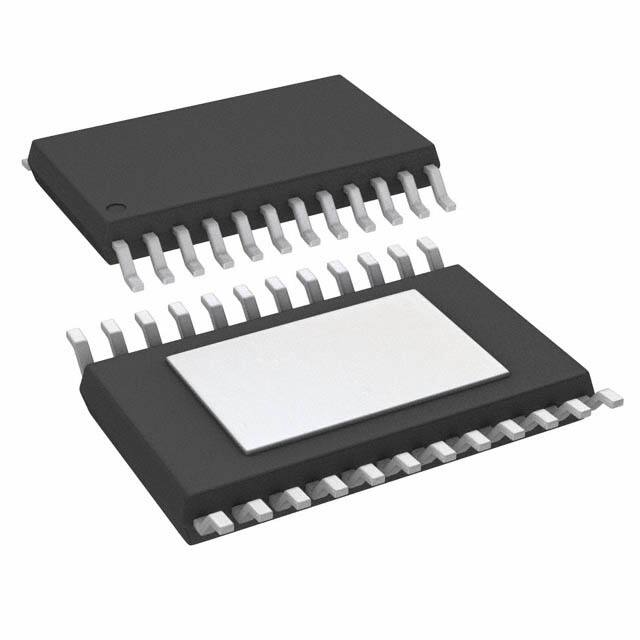


 工商网监
湘ICP备2023018690号
工商网监
湘ICP备2023018690号

