DRV401
SBVS070B − JUNE 2006 − REVISED MAY 2009
Sensor Signal Conditioning IC for
Closed-Loop Magnetic Current Sensor
FEATURES
DESCRIPTION
D DESIGNED FOR SENSORS FROM
D
D
D
D
D
D
D
D
D
VACUUMSCHMELZE (VAC)
SINGLE SUPPLY: 5V
POWER OUTPUT: H-Bridge
DESIGNED FOR DRIVING INDUCTIVE LOADS
EXCELLENT DC PRECISION
WIDE SYSTEM BANDWIDTH
HIGH-RESOLUTION, LOW-TEMPERATURE
DRIFT
BUILT-IN DEGAUSS SYSTEM
EXTENSIVE FAULT DETECTION
EXTERNAL HIGH-POWER DRIVER OPTION
APPLICATIONS
D GENERATOR/ALTERNATOR MONITORING
D
D
D
D
The DRV401 is designed to control and process signals
from specific magnetic current sensors made by
Vacuumschmelze GmbH & Co. KG (VAC). A variety of
current ranges and mechanical configurations are
available. Combined with a VAC sensor, the DRV401
monitors both ac and dc currents to high accuracy.
Provided functions include: probe excitation, signal
conditioning of the probe signal, signal loop amplifier, an
H-bridge driver for the compensation coil, and an analog
signal output stage that provides an output voltage
proportional to the primary current. It offers overload and
fault detection, as well as transient noise suppression.
The DRV401 can directly drive the compensation coil, or
connect to external power drivers. Therefore, the DRV401
combines with sensors to measure small to very large
currents.
To maintain the highest accuracy, the DRV401 can
demagnetize (degauss) the sensor at power-up and on
demand.
AND CONTROL
FREQUENCY AND VOLTAGE INVERTERS
MOTOR DRIVE CONTROLLERS
SYSTEM POWER CONSUMPTION
PHOTOVOLTAIC SYSTEMS
Patents Pending.
Compensation
PWM
ICOMP1
PWM
Compensation Winding
Primary Winding
RS
ICOMP2
DRV401
Diff
Amp
Magnetic Core
Field Probe
IS2
IP
VOUT
REFIN
IS1
Probe
Interface
Integrator
Filter
Timing, Error Detection,
and Power Control
H−Bridge
Driver
Degauss
VREF
VREF
+5V GND
Please be aware that an important notice concerning availability, standard warranty, and use in critical applications of Texas Instruments
semiconductor products and disclaimers thereto appears at the end of this data sheet.
PowerPAD is a trademark of Texas Instruments. All other trademarks are the property of their respective owners.
Copyright 2006−2009, Texas Instruments Incorporated
��������� �
�
��
�������� �� ������� �� �
����������� ����� ��������
���
��� �� �����
�������� ��� ��� ����� �
����� ����������� �������� ���������
���������� ���������! ���� ��� ����������� ������� ������! �
��� �����������
www.ti.com
���"#$%
www.ti.com
SBVS070B − JUNE 2006 − REVISED MAY 2009
ABSOLUTE MAXIMUM RATINGS(1)
Supply Voltage . . . . . . . . . . . . . . . . . . . . . . . . . . . . . . . . . . . . . . . +7V
Signal Input Terminals:
Voltage(2) . . . . . . . . . . . . . . . . . . . . . . . . . . . −0.5V to VDD + 0.5V
Differential Amplifier(3) . . . . . . . . . . . . . . . . . . . . . . −10V to +10V
Current at IS1 and IS2 . . . . . . . . . . . . . . . . . . . . . . . . . . . . . ±75mA
Current (pins other than IS1 and IS2)(2) . . . . . . . . . . . . . . ±25mA
ICOMP Short Circuit(4) . . . . . . . . . . . . . . . . . . . . . . . . . . . . . +250mA
Operating Junction Temperature . . . . . . . . . . . . . −50°C to +150°C
Storage Temperature . . . . . . . . . . . . . . . . . . . . . . . −55°C to +150°C
ESD Rating:
Human Body Model (HBM)
Pins IAIN1 and IAIN2 Only . . . . . . . . . . . . . . . . . . . . . . . . . . . 1kV
All Other Pins . . . . . . . . . . . . . . . . . . . . . . . . . . . . . . . . . . . . . 4kV
(1) Stresses above these ratings may cause permanent damage.
Exposure to absolute maximum conditions for extended periods
may degrade device reliability. These are stress ratings only, and
functional operation of the device at these or any other conditions
beyond those specified is not supported.
(2) Input terminals are diode-clamped to the power-supply rails.
Input signals that can swing more than 0.5V beyond the supply
rails must be current limited, except for the differential amplifier
input pins.
(3) These inputs are not internally protected against over voltage.
The differential amplifier input pins must be limited to 5mA, max or
±10V, max.
(4) Power-limited; observe maximum junction temperature.
2
This integrated circuit can be damaged by ESD. Texas
Instruments recommends that all integrated circuits be
handled with appropriate precautions. Failure to observe
proper handling and installation procedures can cause damage.
ESD damage can range from subtle performance degradation to
complete device failure. Precision integrated circuits may be more
susceptible to damage because very small parametric changes could
cause the device not to meet its published specifications.
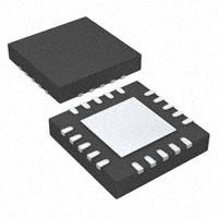
ORDERING INFORMATION(1)
PRODUCT
PACKAGE-LEAD
DRV401
QFN-20
(5mm x 5mm)
PACKAGE
PACKAGE
DESIGNATOR MARKING
RGW
HAAQ
DRV401
SO-20
DWP
DRV401A
(1) For the most current package and ordering information see the
Package Option Addendum at the end of this document, or see
the TI web site at www.ti.com.
���"#$%
www.ti.com
SBVS070B − JUNE 2006 − REVISED MAY 2009
ELECTRICAL CHARACTERISTICS
Boldface limits apply over the specified temperature range: TJ = −40°C to +125°C.
At TA = +25°C and VDD1 = VDD2 = +5V with external 100kHz filter BW, and zero output current ICOMP, unless otherwise noted.
DRV401
PARAMETER
CONDITIONS
DIFFERENTIAL AMPLIFIER
OFFSET VOLTAGE
Offset Voltage, RTO(1)(2)
Drift, RTO(2)
vs Common-Mode, RTO
vs Power-Supply, RTO
VOS
dVOS/dT
CMRR
PSRR
MAX
UNITS
Gain 4V/V
±0.01
±0.1
±50
±4
±0.1
±1(3)
±250
±50
mV
µV/°C
µV/V
µV/V
−1V to +6V, VREF = 2.5V
VREF not included
(VDD) + 1
V
−1
SIGNAL OUTPUT
Signal Over-Range Indication (OVER-RANGE), Delay(2)
Voltage Output Swing From Negative Rail(2),
OVER-RANGE Trip Level
Voltage Output Swing From Positive Rail(2),
OVER-RANGE Trip Level
Short-Circuit Current(2)
ISC
Gain, VOUT/VIN_DIFF
Gain Error
Gain Error Drift
Linearity Error
BW−3dB
SR
VIN = 1V Step, See Notes 2 and 3
2.5 to 3.5
I = +2.5mA, CMP Trip Level
+48
I = −2.5mA, CMP Trip Level
VDD − 85
+85
mV
mV
RL = 1kΩ
−18
+20
4
±0.02
±0.1
10
mA
mA
V/V
%
ppm/°C
ppm
CMVR = −1V to = +4V
dV ± 2V to 1%, No External Filter
dV ± 0.4V to 0.01%
2
6.5
0.9
14
16.5
41
41
en
µs
VDD − 48
VOUT Connected To GND
VOUT Connected To VDD
INPUT RESISTANCE
Differential
Common-Mode
External Reference Input
NOISE
Output Voltage Noise Density, f = 1kHz, RTO(2)
TYP
RL = 10kΩ to 2.5V, VREFIN = 2.5V
SIGNAL INPUT
Common-Mode Voltage Range
FREQUENCY RESPONSE
Bandwidth(2)
Slew Rate(2)
Settling Time, Large-Signal(2)
Settling Time(2)
MIN
20
50
50
±0.3
MHz
V/µs
µs
µs
23.5
59
59
kΩ
kΩ
kΩ
Compensation Loop Disabled
170
nV/√Hz
Probe f = 250kHz, RLOAD = 20Ω
Deviation from 50% PWM, Pin Gain = L
Deviation from 50% PWM, Pin Gain = L
|VICOMP1| − |VICOMP2|
Probe Loop f = 250kHz
0.03
7.5
25
500
%
ppm/°C
ppm/V
ppm/V
COMPENSATION LOOP
DC STABILITY
Offset Error(4)
Offset Error Drift(2)
Gain, Pin Gain = L(2)
Power-Supply Rejection Ratio
PSRR
FREQUENCY RESPONSE
Open-Loop Gain, Two Modes, 7.8kHz
Pin Gain H/L
PROBE COIL LOOP
Input Voltage Clamp Range
RHIGH
Internal Resistor, IS1 or IS2 to GND1(2)
Resistance Mismatch Between IS1 and IS2(2)
Total Input Resistance(3)
Comparator Threshold Current(3)
Minimum Probe Loop Half-Cycle(2)
Probe Loop Minimum Frequency
No Oscillation Detect (Error) Suppression
RLOW
−0.7 to VDD + 0.7
V
59
71
Ω
60
75
300
134
28
280
90
1500
200
34
310
Ω
ppm
W
mA
ns
kHz
22
250
250
ICOMP1 and ICOMP2 Railed
dB
47
ppm of RHIGH + RLOW
VICOMP1 − VICOMP2 = 4.0VPP
20Ω Load
200
24/32
Field Probe Current < 50mA
Internal Resistor, IS1 or IS2 to VDD1(2)
COMPENSATION COIL DRIVER, H-BRIDGE
Peak Current(2)
Voltage Swing
Output Common-Mode Voltage
Wire Break Detect, Threshold Current(5)
−200
35
µs
250
mA
VPP
V
mA
4.2
VDD2/2
33
57
3
���"#$%
www.ti.com
SBVS070B − JUNE 2006 − REVISED MAY 2009
ELECTRICAL CHARACTERISTICS (continued)
Boldface limits apply over the specified temperature range, TJ = −40°C to +125°C, with zero output current ICOMP.
At TA = +25°C and VDD1 = VDD2 = +5V with external 100kHz filter BW, unless otherwise noted.
DRV401
PARAMETER
VOLTAGE REFERENCE
Voltage(2)
Drift(2)
PSRR(2)
Load Regulation(2)
Short-Circuit Current
ISC
DEMAGNETIZATION
Duration
CONDITIONS
MIN
TYP
MAX
UNITS
No Load
No Load
2.495
2.505
±50
±200
Load to GND/VDD, dI = 0mA to 5mA
REFOUT Connected to VDD
REFOUT Connected to GND
2.5
±5
±15
0.15
+20
−18
V
ppm/°C
µV/V
mV/mA
mA
mA
See Timing Diagram
106
130(3)
ms
5
µA
µA
µA
V
V
DIGITAL I/O
LOGIC INPUTS (DEMAG, GAIN, and CCdiag Pins)
Pull-Up High Current (CCdiag)
Pull-Up Low Current (CCdiag)
Logic Input Leakage Current
Logic Level, Input: L/H
Hysteresis
CMOS Type Levels
3.5 < VIN < VDD
0 < VIN < 1.5
0 < VIN < VDD
OUTPUTS (ERROR AND OVER-RANGE Pins)
Logic Level, Output: L
Logic Level, Output: H
4mA Sink
OUTPUTS (PWM and PWM Pins)
Logic Level L
Logic Level H
POWER SUPPLY
Specified Voltage Range
Power-On Reset Threshold
Quiescent Current [I(VDD1) + I(VDD2)]
Brownout Voltage Level(2)
Brownout Indication Delay
TEMPERATURE RANGE
Specified Range
Operating Range
Package Thermal Resistance
QFN Surface-Mount
SO PowerPAD Surface-Mount
(1)
(2)
(3)
(4)
(5)
(6)
4
160
5
0.01
2.1/2.8
0.7
Push-Pull Type
4mA Sink
4mA Source
VDD
VRST
IQ
4.5
0.3
No Internal Pull-Up
V
0.2
(VDD) − 0.4
V
V
5
1.8
6.8
V
V
mA
V
µs
−40
+125
°C
−50
+150
°C
ICOMP = 0mA, Sensor Not Connected
5.5
4
135
TJ
TJ
qJA
See Note 6
40
°C/W
qJA
See Note 6
27
°C/W
Parameter value referred to output (RTO).
See Typical Characteristic curves.
Total input resistance and comparator threshold current are inversely related. See Figure 2a.
For VAC sensors, 0.2% of PWM offset approximately corresponds to 10mA primary current offset per winding.
See Compensation Driver section in Applications Information.
See Applications Information section for information on power dissipation, layout considerations, and proper PCB soldering and heat-sinking technique.
���"#$%
www.ti.com
SBVS070B − JUNE 2006 − REVISED MAY 2009
PIN CONFIGURATIONS
IS2
16
GND1
17
IS1
18
ERROR
3
18
IS2
DEMAG
4
17
VDD1
16
OVER−RANGE
15
CCdiag
14
VDD2
10
Exposed
Thermal Pad
on Underside,
Connect
to GND1
ICOMP2
5
GND1
9
REFIN
19
GND2
4
2
8
REFOUT
PWM
IAIN1
3
IS1
7
GAIN
20
IAIN2
2
19
20
DEMAG
DWP
1
6
1
Top View
PWM
VOUT
ERROR
PWM
RGW
PWM
Top View
15
VDD1
14
OVER−RANGE
13
CCdiag
12
VDD2
11
ICOMP1
Exposed
Thermal Pad
on Underside,
Connect
to GND1
GAIN
5
REFOUT
6
REFIN
7
VOUT
8
13
ICOMP1
IAIN2
9
12
ICOMP2
IAIN1
10
11
GND2
QFN−20 (5mm x 5mm)
Wide−Body SO−20
PIN ASSIGNMENTS
NAME
RGW
DWP
ERROR
1
3
DESCRIPTION
Error flag: open-drain output, see the Error Conditions section.
DEMAG
2
4
Control input, see the Demagnetization section.
GAIN
3
5
Control input for open-loop gain: low = normal, high = −8dB.
REFOUT
4
6
Output for internal 2.5V reference voltage.
REFIN
5
7
Input for zero reference to differential amplifier.
VOUT
6
8
Output for differential amplifier.
IAIN2
7
9
Noninverting input of differential amplifier.
IAIN1
8
10
Inverting input of differential amplifier.
GND2
9
11
Ground connection. Connect to GND1.
ICOMP2
10
12
Output 2 of compensation coil driver.
ICOMP1
11
13
Output 1 of compensation coil driver.
VDD2
12
14
Supply voltage. Connect to VDD1.
CCdiag
13
15
Control input for wire-break detection: high = enable.
OVER−RANGE
14
16
Open-drain output for over-range indication: low = over-range.
VDD1
15
17
Supply voltage.
IS2
16
18
Probe connection 2.
GND1
17
19
Ground connection.
IS1
18
20
Probe connection 1.
PWM
19
1
PWM output from probe circuit (inverted).
PWM
20
2
PWM output from probe circuit.
Exposed Thermal Pad
—
—
Connect to GND1.
5
���"#$%
www.ti.com
SBVS070B − JUNE 2006 − REVISED MAY 2009
TYPICAL CHARACTERISTICS
At TA = +25°C and VDD1 = VDD2 = +5V with external 100kHz filter BW, unless otherwise noted.
DRV401 AND SENSOR:
OUTPUT VOLTAGE NOISE DENSITY
(Sensor M4645−X080, RSHUNT = 10Ω, Mode = Low)
DRV401 AND SENSOR:
OFFSET vs SUPPLY VOLTAGE
0.04
100
0.03
60Hz Line Frequency and Multiples
(measured in a 60Hz environment)
0.02
IPRIM (A)
VN (µV/√Hz)
M4645−X211
M4645−X211
0.01
0
M4645−X080
−0.01
Divided Field
Probe Frequency
10
−0.02
−0.03
−0.04
0.1
4.1
4.5
4.3
4.7
4.9
5.1
5.5
5.7
5.9
6.1
0.1
1
10
100
1k
10k
VDD (V)
Frequency (Hz)
DRV401 AND SENSOR: ABSOLUTE ERROR
(Soldered DWP−20 with 1 Square−Inch Copper Pad)
(Measurements by Vacuumschmelza GmbH)
GAIN FLATNESS vs FREQUENCY
(Measurements by Vacuumschmelze GmbH)
0.3
100k
1.20
T = −50_ C
T = +25_C
T = +85_C
T = +125_ C
DRV401 with M4645−X600 Sensor
DRV401 with M4645−X211 Sensor
DRV401 with M4645−X080 Sensor
1.15
1.10
Normalized Gain
0.2
Absolute Error (A)
5.3
0.1
0
−0.1
1.05
1.00
0.95
0.90
−0.2
0.85
TC (RSHUNT) ±25ppm/_ C.
−0.3
−300
−200
0.80
−100
0
100
200
300
10
Primary Current (A)
100
1k
10k
100k
Frequency (Hz)
DIFFERENTIAL AMPLIFIER:
VOLTAGE OFFSET PRODUCTION DISTRIBUTION
3A ICOMP OVERLOAD RECOVERY
(Measurements by Vacuumschmelze GmbH)
RTO
Over−Range
VOUT
ERROR
Population
2V/div
VOUT
2000A/div
Over−Range
ERROR
0
20
40
60
80
100 120 140 160 180 200
Time (µs)
6
IPRIM
−50
−45
−40
−35
−30
−25
−20
−15
−10
−5
0
5
10
15
20
25
30
35
40
45
50
IPRIM
NOTE: IPRIM = 3000A corresponds to ICOMP = 3A.
Voltage Offset (µV)
1M
���"#$%
www.ti.com
SBVS070B − JUNE 2006 − REVISED MAY 2009
TYPICAL CHARACTERISTICS (Continued)
At TA = +25°C and VDD1 = VDD2 = +5V with external 100kHz filter BW, unless otherwise noted.
DIFFERENTIAL AMPLIFIER:
GAIN vs FREQUENCY
DIFFERENTIAL AMPLIFIER:
OFFSET VOLTAGE vs TEMPERATURE, RTO
20
20
16
15
10
8
Gain (dB)
Input VOS (µV)
12
4
Sample Average
0
−4
−8
5
0
−5
−10
−12
−15
−16
−20
−50
−20
−25
0
25
50
75
100
125
100
10
150
1k
10k
DIFFERENTIAL AMPLIFIER:
PSRR AND CMRR vs FREQUENCY
DIFFERENTIAL AMPLIFIER:
OUTPUT VOLTAGE vs OUTPUT CURRENT
5.0
−40_ C
PSRR
+25_C
Output Voltage (V)
CMRR
80
60
40
+125_ C
4.8
+85_ C
4.7
0.3
+85_C
+125_C
0.2
20
0.1
0
0
−40_C
+25_ C
10
100
1k
10k
100k
1M 2M
0
1
2
3
Frequency (Hz)
4
5
6
25
Short−Circuit Current (mA)
100
Autozero Frequency = 69kHz
Sensor Not Running
en = 162nV/√Hz (average over 250Hz to 50kHz)
10k
Frequency (Hz)
9
10
VOUT Shorted to 5V
20
1k
8
DIFFERENTIAL AMPLIFIER:
SHORT−CIRCUIT CURRENT vs TEMPERATURE
1000
100
7
Load Current (mA)
DIFFERENTIAL AMPLIFIER:
OUTPUT NOISE DENSITY
Noise Density (nV/√Hz)
10M
4.9
100
10
1M
Frequency (Hz)
120
PSRR and CMRR (dB)
100k
Temperature (_C)
100k
15
10
5
0
−5
−10
−15
−20
1M
−25
−50
VOUT Shorted to 0V
−25
0
25
50
75
100
125
150
Temperature (_ C)
7
���"#$%
www.ti.com
SBVS070B − JUNE 2006 − REVISED MAY 2009
TYPICAL CHARACTERISTICS (Continued)
At TA = +25°C and VDD1 = VDD2 = +5V with external 100kHz filter BW, unless otherwise noted.
DIFFERENTIAL AMPLIFIER:
TA = +25_C LARGE−SIGNAL STEP RESPONSE
3.8
3.8
3.6
3.4
3.6
3.4
3.2
3.2
3.0
3.0
Voltage (V)
Voltage (V)
DIFFERENTIAL AMPLIFIER:
TA = −50_C LARGE−SIGNAL STEP RESPONSE
2.8
2.6
2.4
2.8
2.6
2.4
2.2
2.2
2.0
2.0
1.8
1.6
1.8
1.6
1.4
1.4
1µs/div
1µs/div
DIFFERENTIAL AMPLIFIER:
OVER−RANGE DELAY vs TEMPERATURE
3.8
3.5
3.6
3.4
3.4
3.2
3.3
Over−Range Delay (µs)
Voltage (V)
DIFFERENTIAL AMPLIFIER:
TA = +150_C LARGE−SIGNAL STEP RESPONSE
3.0
2.8
2.6
2.4
2.2
2.0
1.8
1.6
3.2
At 5.0V
VIN Step 0V to ±1V
Negative Over−Range
3.1
3.0
2.9
Positive Over−Range
2.8
2.7
2.6
1.4
2.5
1µs/div
−50
−25
0
25
50
75
100
125
150
Temperature (_ C)
DIFFERENTIAL AMPLIFIER:
POSITIVE SLEW RATE vs TEMPERATURE
−6.5
At 5.0V
7.4
−6.6
7.3
−6.7
7.2
−6.8
Slew Rate (V/µs)
Slew Rate (V/µs)
7.5
7.1
7.0
6.9
6.8
−7.0
−7.1
−7.2
−7.3
6.6
−7.4
−50
−25
0
25
50
75
Temperature (_ C)
100
125
150
At 5.0V
−6.9
6.7
6.5
8
DIFFERENTIAL AMPLIFIER:
NEGATIVE SLEW RATE vs TEMPERATURE
−7.5
−50
−25
0
25
50
75
Temperature (_ C)
100
125
150
���"#$%
www.ti.com
SBVS070B − JUNE 2006 − REVISED MAY 2009
TYPICAL CHARACTERISTICS (Continued)
At TA = +25°C and VDD1 = VDD2 = +5V with external 100kHz filter BW, unless otherwise noted.
Gain VPWMAVERAGE /(VICOMP1, VICOMP2) (dB)
DIFFERENTIAL AMPLIFIER:
REFIN RESISTANCE vs TEMPERATURE
50.250
RREF IN (kΩ )
50.125
50.000
49.875
49.750
49.625
−50
−25
0
25
50
75
100
125
COMPENSATION LOOP:
SMALL−SIGNAL GAIN
70
60
50
Pin Gain = Low
40
Pin Gain = High
30
20
10
0
150
100
10k
100k
Frequency (Hz)
COMPENSATION LOOP:
DUTY CYCLE ERROR vs TEMPERATURE
COMPENSATION LOOP:
DC GAIN: DUTY CYCLE ERROR CHANGE
2000
VICOMP1 − VICOMP2 = 4.2V
ILOAD = 210mA
1500
Gain Pin Low
1000
500
Population
Duty Cycle Error (ppm)
1k
Temperature (_ C)
0
At 250kHz, 5.0V
−500
−1000
At 400kHz, 5.0V
−2000
−50
−25
0
25
50
75
100
125
−200
−180
−160
−140
−120
−100
−80
−60
−40
−20
0
20
40
60
80
100
120
140
160
180
200
−1500
150
Temperature (_ C)
Gain (ppm/V)
ICOMP OUTPUT SWING TO RAIL
vs OUTPUT CURRENT
5.00
4.75
+125_C
Output Swing (V)
4.50
−50_ C
+25_ C
4.25
4.00
1.00
0.75
0.50
+125_C +25_ C
0.25
−50_ C
0
0
50
100
150
200
Output Current (mA)
250
300
Probe Comparator Threshold Current (mA)
PROBE COMPARATOR THRESHOLD
CURRENT vs TEMPERATURE
35.0
32.5
30.0
27.5
25.0
−50
−25
0
25
50
75
100
125
150
Temperature (_ C)
9
���"#$%
www.ti.com
SBVS070B − JUNE 2006 − REVISED MAY 2009
TYPICAL CHARACTERISTICS (Continued)
At TA = +25°C and VDD1 = VDD2 = +5V with external 100kHz filter BW, unless otherwise noted.
PROBE DRIVER:
INTERNAL RESISTOR vs TEMPERATURE
OUTPUT IMPEDANCE MISMATCH OF IS1 AND IS2
vs TEMPERATURE
90
Output Impedance Mismatch (Ω )
0.10
85
80
Resistance (Ω)
Driver L
75
70
65
60
Driver H
55
50
45
−50
−25
0.08
0.06
0.04
0.02
0
0
25
50
75
100
125
150
−50
−25
0
25
50
75
100
125
150
Temperature (_ C)
Temperature (_ C)
VOLTAGE REFERENCE vs LOAD CURRENT
VOLTAGE REFERENCE PRODUCTION DISTRIBUTION
2.5010
2.5008
2.5006
Population
VREF (V)
2.5004
2.5002
2.5000
2.4998
2.4996
2.4994
2.4992
−6
−4
−2
0
2
4
6
2.4950
2.4955
2.4960
2.4965
2.4970
2.4975
2.4980
2.4985
2.4990
2.4995
2.5000
2.5005
2.5010
2.5015
2.5020
2.5025
2.5030
2.5035
2.5040
2.5045
2.5050
2.4990
ILOAD (mA)
VREF (V)
VOLTAGE REFERENCE DRIFT
PRODUCTION DISTRIBUTION
VOLTAGE REFERENCE vs TEMPERATURE
2.525
2.520
2.515
VREF (V)
Population
2.510
2.505
2.500
2.495
2.490
2.485
0
2.5
5.0
7.5
10.0
12.5
15.0
17.5
20.0
22.5
25.0
27.5
30.0
32.5
35.0
37.5
40.0
42.5
45.0
47.5
50.0
2.480
Voltage Reference Drift (ppm/_ C)
10
2.475
−50
−25
0
25
50
75
Temperature (_ C)
100
125
150
���"#$%
www.ti.com
SBVS070B − JUNE 2006 − REVISED MAY 2009
TYPICAL CHARACTERISTICS (Continued)
At TA = +25°C and VDD1 = VDD2 = +5V with external 100kHz filter BW, unless otherwise noted.
VOLTAGE REFERENCE POWER−SUPPLY REJECTION
PRODUCTION DISTRIBUTION
250
253
256
259
262
265
268
271
274
277
280
283
286
289
292
295
298
301
304
307
310
200
175
150
125
75
100
50
0
25
−25
−50
−75
−100
−125
−150
−175
−200
Population
Population
OSCILLATOR PRODUCTION DISTRIBUTION
Minimum Probe Loop Half−Cycle (ns)
PSR (µV/V)
OSCILLATOR vs SUPPLY VOLTAGE
OSCILLATOR vs TEMPERATURE
Minimum Probe Loop Half−Cycle (ns)
305
300
295
290
285
280
275
270
265
260
255
250
−50
−25
0
25
50
75
100
125
310
305
300
295
290
285
280
275
270
265
260
255
250
4.3
150
4.9
4.6
5.2
5.5
5.8
6.0
VDD (V)
Temperature (_C)
BROWN−OUT VOLTAGE vs TEMPERATURE
4.20
4.15
Brown−Out Voltage (V)
Minimum Probe Loop Half−Cycle (ns)
310
4.10
4.05
4.00
3.95
3.90
3.85
3.80
−50
−25
0
25
50
75
100
125
150
Temperature (_ C)
11
���"#$%
www.ti.com
SBVS070B − JUNE 2006 − REVISED MAY 2009
APPLICATIONS INFORMATION
FUNCTIONAL PRINCIPLE OF CLOSED-LOOP
CURRENT SENSORS WITH MAGNETIC
PROBE USING THE DRV401
Closed-loop current sensors measure current over wide
frequency ranges, including dc. These types of devices
offer a contact-free method as well as excellent galvanic
isolation performance combined with high resolution,
accuracy, and reliability.
At dc and in low-frequency ranges, the magnetic field
induced from the current in the primary winding is
compensated by a current flowing through a
compensation winding. A magnetic field probe, located in
the magnetic core loop, detects the magnetic flux. This
probe delivers the signal to the amplifier that drives the
current through the compensation coil, bringing the
magnetic flux back to zero. This compensation current is
proportional to the primary current, relative to the winding
ratio.
In higher frequency ranges, the compensation winding
acts as the secondary winding in the current transformer,
while the H-bridge compensation driver is rolled off and
provides low output impedance.
A difference amplifier senses the voltage across a small
shunt resistor that is connected to the compensation loop.
This difference amplifier generates the output voltage that
is referenced to REFIN and is proportional to the primary
current. Figure 1 shows the DRV401 used as a
compensation current sensor.
Compensation
RS
ICOMP1
Compensation Winding
Primary Winding
ICOMP2
DRV401
Diff
Amp
Magnetic Core
Field Probe
IS2
IP
VOUT
REFIN
IS1
Probe
Interface
Integrator
Filter
Timing, Error Detection,
and Power Control
H−Bridge
Driver
Degauss
VREF
+5V GND
Figure 1. Principle of Compensation Current Sensor with the DRV401
12
VREF
���"#$%
www.ti.com
SBVS070B − JUNE 2006 − REVISED MAY 2009
FUNCTIONAL DESCRIPTION
The DRV401 operates from a single +5V supply. It is a
complete sensor signal conditioning circuit that directly
connects to the current sensor, providing all necessary
functions for the sensor operation. The DRV401 provides
magnetic field probe excitation, signal conditioning, and
compensation coil driver amplification. In addition, it
detects error conditions and handles overload situations.
A precise differential amplifier allows translation of the
compensation current into an output voltage using a small
shunt resistor. A buffered voltage reference can be used
for comparator, analog-to-digital converter (ADC), or
bipolar zero reference voltages.
Dynamic error correction ensures high dc precision over
temperature and long-term accuracy. The DRV401 uses
analog signal conditioning; the internal loop filter and
integrator are switched capacitor-based circuits.
Therefore, the DRV401 allows combination with
high-precision sensors for exceptional accuracy and
resolution. The typical characteristic curve, DRV401 and
Sensor Linearity, shows an example of the linearity and
temperature stability achieved by the device.
A demagnetization cycle can be initiated on demand or on
power-up. This cycle reduces offset and restores high
performance after a strong overload condition. An internal
clock and counter logic generate the degauss function.
The same clock controls power-up, overload detection and
recovery, error, and time-out conditions.
The DRV401 is built on a highly reliable CMOS process.
Unique protection cells at critical connections enable the
design to handle inductive energy.
MAGNETIC PROBE (SENSOR) INTERFACE
The magnetic field probe consists of an inductor wound on
a soft magnetic core. The probe is connected between
pins IS1 and IS2 of the probe driver that applies
approximately +5V (the supply voltage) through resistors
across the probe coil (see Figure 2a).
The probe core reaches saturation at a current of typically
28mA (see Figure 2a). The comparator is connected to
VREF by approximately 0.5V. A current comparator detects
the saturation and inverts the excitation voltage polarity,
causing the probe circuit to oscillate in a frequency range
of 250kHz to 550kHz. The oscillating frequency is a
function of the magnetic properties of the probe core and
its coil.
The current rise rate is a function of the coil inductance:
dI = L × V × dT. However, the inductance of the field probe
is low while its core material is in saturation (the horizontal
part of the hysteresis curve) and is high at the vertical part
of the hysteresis curve. The resulting inductance and the
series resistance determine the output voltage and current
versus time performance characteristic.
Without external magnetic influence, the duty cycle is
exactly 50% because of the inherent symmetry of the
magnetic hysteresis; the probe inductor is driven from −B
saturation through the high inductance range to +B
saturation and back again in a time-symmetric manner
(see Figure 2b).
If the core material is magnetized in one direction, a long
and a short charge time result because the probe current
through the inductors generates a field that either
subtracts or adds to the flux in the probe core, either driving
the probe core out of saturation or further into saturation
(see Figure 2c). The current into the probe is limited by the
voltage drops across the probe driver resistors.
The DRV401 continuously monitors the logic magnetic flux
polarity state. In the case of distortion noise and excessive
overload that could fully saturate the probe, the overload
control circuit recovers the probe loop. During an overload
condition, the probe oscillation frequency increases to
approximately 1.6MHz until limited by the internal timing
control.
In an overload condition, the compensation current (ICOMP)
driver cannot deliver enough current into the sensor
secondary winding, and the magnetic flux in the sensor
main core becomes uncompensated.
13
���"#$%
www.ti.com
SBVS070B − JUNE 2006 − REVISED MAY 2009
VDD1
Probe
55Ω
55Ω
IS2
IS1
CMP
18Ω
PWM
VREF = 0.5V
NOTE: MOS components function as switches only.
a) Simplified probe interface circuit.
The probe is connected between S1 and S2.
B
B
2V/div
V (IS1)
2V/div
V (IS1)
V (PWM)/10
500mV/div
H
500mV/div
H
V (PWM)/10
500ns/div
b) Without an external magnetic field, the hysteresis curve is
symmetrical and the probe loop generates 50% duty cycle.
500ns/div
c) An external magnetic flux (H) generated from the primary current
(IPRIM) shifts the hysteresis curve of the magnetic field probe in the
H-axis and the probe loop generates a nonsymmetrical duty cycle.
Figure 2. Magnetic Probe, Hysteresis, and Duty Cycle
14
���"#$%
www.ti.com
SBVS070B − JUNE 2006 − REVISED MAY 2009
The transition from normal operation to overload happens
relatively slowly, because the inherent sensor transformer
characteristics induce the initial primary current step, as
shown in Figure 3. As the transformer-induced secondary
current starts to decay, the compensation feedback driver
increases its output voltage to maintain the sensor core
flux compensation at zero.
When the system compensation loop reaches its driving
limit, the rising magnetic flux causes one of the probe
PWM half-periods to become shorter. The minimum
half-period of the probe oscillation is limited by the internal
timing to 280ns, based on the properties of the VAC
magnetic sensors. After three consecutive cycles of the
same half-period being shorter than 280ns, the DRV401
goes into overload-latch mode. The device stores the
ICOMP driver output signal polarity and continues producing
the skewed-duty cycle PWM signal. This action prevents
the loss of compensation signal polarity information during
very strong overloads. In this case, both PWM half-periods
are short and approximately equal, because the field
probe stays completely in one of the saturated regions.
The overload-latch condition is removed after the primary
current goes low enough for the ICOMP driver to
compensate, and both half-periods of the probe driver
oscillation become longer than 280ns (the field probe
comes out of the saturated region).
Peak voltages and currents can be generated during
normal operations as well as overload conditions.
Therefore, both probe connection pins are internally
For reliable operation, error detection circuits monitor the
probe operation:
1. If the probe driver comparator (CMP) output stays low
longer than 32µs, the ERROR flag asserts active, and
the compensation current (ICOMP) is set to zero.
2. If the probe driver period is less than 275ns on three
consecutive pulses, the ERROR flag asserts active.
See the Error Conditions section for more details.
PWM PROCESSING
The outputs PWM and PWM represent the probe output
signal as a differential PWM signal. It can drive external
circuitry or be used for synchronous ripple reduction. The
PWM signal from the probe excitation and sense stage is
internally
connected
to
a
high-performance,
switched-capacitor
integrator
followed
by
an
integrating-differentiating filter. This filter converts the
PWM signal into a filtered delta signal and prepares it for
driving the analog compensation coil driver. The gain
roll-off frequency of the filter stage is set to provide high dc
gain and loop stability. If additional gain is added from
external circuitry, the internal gain can be reduced by 8dB,
asserting the GAIN pin high (see the External
Compensation Coil Driver section).
V(1Ω× IPRIM/10)
1
I COMP1
3
4
protected against coupled energy from the magnetic core.
Wiring between probe and IC inputs should be short and
guarded against interference; see Layout Considerations.
Sensor: 4 x 100
RSH = 10Ω
Step Response
2kHz In
V(Gain) = Low
ICOMP2
Channel 1: 2V/div
Channels 2−4: 500mV/div
2
VOUT
50µs/div
A current pulse of 0A to 18A (Ch 1) generates the two ICOMP signals (Ch 3 and Ch 4). Ch 2 shows the resulting output signal,
VOUT. This test uses the M4645-X030 sensor, no bandwidth limitation, but a 20-sample average.
Figure 3. Primary Current Step Response
15
���"#$%
www.ti.com
SBVS070B − JUNE 2006 − REVISED MAY 2009
COMPENSATION DRIVER
For sensors with high winding resistance (compensation coil
resistance + RSHUNT) or connected to an external
compensation driver, this function should be disabled by
pulling the CCdiag pin low.
The compensation coil driver provides the driving current
for the compensation coil. A fully differential driver stage
offers high signal voltages to overcome the wire resistance
of the coil with only +5V supply. The compensation coil is
connected between ICOMP1 and ICOMP2, both generating an
analog voltage across the coil (see Figure 3) that turns into
current from the wire resistance (and eventually from the
inductance). The compensation current represents the
primary current transformed by the turns ratio. A shunt
resistor is connected in this loop and the high-precision
difference amplifier translates the voltage from this shunt
to an output voltage.
R MAX +
V OUT
65mA
Where:
VOUT equals the peak voltage between ICOMP1 and ICOMP2
at a 65mA drive current.
RMAX equals the sum of the coil and the shunt resistance.
EXTERNAL COMPENSATION COIL DRIVER
Both compensation driver outputs provide low impedance
over a wide frequency range to insure smooth transitions
between the closed-loop compensation frequency range
and the high-frequency range, where the primary winding
directly couples the primary current into the compensation
coil at a rate set by the winding ratio.
An external driver for the compensation coil can be
connected to the ICOMP1 and ICOMP2 outputs. To prevent a
wire break indication, CCdiag has to be asserted low.
An external driver can provide both a higher drive voltage
and more drive current. It also moves the power
dissipation to the external transistors, thereby allowing a
higher winding resistance in the compensation coil and
more current. Figure 4 shows a block diagram of an
external compensation coil driver. To drive the buffer,
either one or both ICOMP outputs can be used. Note,
however, that the additional voltage gain could cause
instability of the loop. Therefore, the internal gain can be
reduced by approximately 8dB by asserting the GAIN pin
high. RSHUNT is connected to GND to allow for a
single-ended external compensation driver. The
differential amplifier can continue to sense the voltage,
and used for the gain and over-range comparator or
ERROR flag.
The two compensation driver outputs are designed with
protection circuitry to handle inductive energy. However,
additional external protection diodes might be necessary
for high current sensors.
For reliable operation, a wire break in the compensation
circuit can be detected. If the feedback loop is broken, the
integrating filter drives the outputs ICOMP1 and ICOMP2 to the
opposite rails. With one of these pins coming within 300mV
to ground, a comparator tests for a minimum current flowing
between ICOMP1 and ICOMP2. If this current stays below the
threshold current level for at least 100µs, the ERROR pin is
asserted active (low). The threshold current level for this test
is less than 57mA at 25°C and 65mA at −40°C, if the ICOMP
pins are fully railed (see the Typical Characteristics).
V+
DRV401
ICOMP1
External
Buffer
Compensation
Coil
ICOMP2
V−
RSHUNT
Figure 4. DRV401 with External Compensation Coil Driver and RSHUNT Connected to GND
16
(1)
���"#$%
www.ti.com
SBVS070B − JUNE 2006 − REVISED MAY 2009
SHUNT SENSE AMPLIFIER
The differential (H-bridge) driver arrangement for the
compensation coil requires a differential sense amplifier
for the shunt voltage. This differential amplifier offers wide
bandwidth and a high slew rate for fast current sensors.
Excellent dc stability and accuracy result from an
auto-zero technique. The voltage gain is 4V/V, set by
precisely matched and stable internal SiCr resistors.
Both inputs of the differential amplifier are normally
connected to the current shunt resistor. This resistor adds
to the internal (10kΩ) resistor, slightly reducing the gain in
this leg. For best common-mode rejection (CMR), a
dummy shunt resistor (R5) is placed in series with the
REFIN pin to restore matching of both resistor dividers, as
shown in Figure 5a.
For gains of 4V/V:
4+
R2
R4 ) R5
+
R1
RSHUNT ) R3
(2)
With R2/R1 = R4/R3 = 4; R5 = RSHUNT × 4
ICOMP2
Typically, the gain error resulting from the resistance of
RSHUNT is negligible; for 70dB of common-mode rejection,
however, the match of both divider ratios needs to be better
than 1/3000.
The amplifier output can drive close to the supply rails, and
is designed to drive the input of a SAR-type ADC; adding
an RC low-pass filter stage between the DRV401 and the
ADC is recommended. This filter not only limits the signal
bandwidth but also decouples the high-frequency
component of the converter input sampling noise from the
amplifier output. For RF and CF values, refer to the specific
converter recommendations in the specific product data
sheet. Empirical evaluation may be necessary to obtain
optimum results.
The output can drive 100pF directly and shows 50%
overshoot with approximately 1nF capacitance. Adding RF
allows much larger capacitive loads, as shown in
Figure 5b and Figure 5c. Note that with RF of only 20Ω, the
load capacitor should be either smaller than 1nF or larger
than 33nF to avoid overshoot; with RF of 50Ω this transient
area is avoided.
DRV401 Differential Amplifier Section
R1
10kΩ
R2
40kΩ
Decoupling, Low−Pass Filter
RF
50Ω
VOUT
R SHUNT
ADC
Differential
Amplifier
R3
10kΩ
K2
R4
40kΩ
REFIN
R5
Dummy
Shunt
CF
10nF
Compensated
REFIN
NOTE: R5 is a dummy shunt resistor equal to 4x RSHUNT to compensate for RSHUNT and provide best CMR.
20mV/div
20mV/div
a) Internal difference amplifier with an example of a decoupling filter.
10µs/div
10µs/div
b) VOUT of Figure 5a with R5 = 20Ω and CD = 100nF.
c) VOUT of Figure 5a with R5 = 50Ω and CD = 10nF.
Figure 5. Internal Difference Amplifier with Example of a Decoupling Filter
17
���"#$%
www.ti.com
SBVS070B − JUNE 2006 − REVISED MAY 2009
The reference input (REFIN) is the reference node for the
exact output signal (VOUT). Connecting REFIN to the
reference output (REFOUT) results in a live zero reference
voltage of 2.5V. Using the same reference for REFIN and
the ADC avoids mismatch errors that exist between two
reference sources.
OVER-RANGE COMPARATOR
High peak current can overload the differential amplifier
connected to the shunt. The OVER-RANGE pin, an
open-drain output, indicates an over-voltage condition for
the differential amplifier by pulling low. The output of this
flag is suppressed for 3µs, preventing unwanted triggering
from transients and noise. This pin returns to high as soon
as the overload condition is removed (external pull-up
required to return the pin high).
This ERROR flag not only provides a warning about a
signal clipping condition, but is also a window comparator
output for actively shutting off circuits in the system. The
value of the shunt resistor defines the operating window for
the current. It sets the ratio between the nominal signal and
the trip level of the Over-Range flag. The trip current of this
window comparator is calculated using the following
example:
With a 5V supply, the output voltage swing is
approximately
±2.45V
(load
and
supply
voltage-dependent).
The gain of 4V/V allows an input swing of ±0.6125V.
Thus, the clipping current is IMAX = 0.6125V/RSHUNT.
See the differential amplifier curve of the Typical
Characteristics, Output Voltage vs Output Current.
The over-range condition is internally detected as soon as
the amplifier exceeds its linear operating range, not just a
set voltage level. Therefore, the error or the over-range
comparator level is reliably indicated in fault conditions
such as output shorts, low load or low supply conditions.
As soon as the output cannot drive the voltage higher, the
flag is activated. This configuration is a safety
improvement over a voltage level comparator.
NOTE: The internal resistance of the compensation coil
may prevent high compensation current from flowing
because of ICOMP driver overload. Therefore, the
differential amplifier may not overload with this current.
However, a fast rate of change of the primary current would
be transmitted through transformer action and safely
trigger the overload flag.
VOLTAGE REFERENCE
The precision 2.5V reference circuit offers low drift
(typically 10ppm/K) and is used for internal biasing; it is
also connected to the REFOUT pin. The circuit is intended
as the reference point of the output signal to allow a bipolar
signal around it. This output is buffered for low impedance
and tolerates sink and source currents of ±5mA.
Capacitive loads can be directly connected, but generate
ringing on fast load transients. A small series resistor of a
few ohms improves the response, especially for a
capacitive load in the range of 1µF. Figure 6 shows the
transient load regulation with 1nF direct load.
The reference source is part of the integrated circuit and
referenced to GND2. Large current pulses driving the
compensation coil can generate a voltage drop in the GND
connection that would add on to the reference voltage.
Therefore, a low impedance GND layout is critical to
handle the currents and the high bandwidth of this IC.
Test Circuit:
±5V
1nF
10mV/div
10kΩ
REFOUT
+2.5V
2.5µs/div
Figure 6. Pulse Response Test Circuit and Scope Shot of Reference
18
���"#$%
www.ti.com
SBVS070B − JUNE 2006 − REVISED MAY 2009
DEMAGNETIZATION
Iron cores are not immune to residual (remanence)
magnetism. The residual remanence can produce a signal
offset error, especially after strong current overload, which
goes along with high magnetic field density. Therefore, the
DRV401 includes a signal generator for a demagnetization
cycle. The digital control pin, DEMAG, starts this cycle on
demand after this pin is held high for at least 25.6µs.
Shorter pulses are ignored. The cycle lasts for
approximately 110ms. During this time, the Error flag is
asserted low to indicate that the output is not valid. When
DEMAG is high during power-on, a demagnetization cycle
immediately initiates (12µs) after power-on (VDD > 4V).
Holding DEMAG low avoids this cycle at power-up (see
the Power-On and Brownout section).
The probe circuit is in normal operation and oscillates
during the demagnetization cycle. The outputs PWM and
PWM are active accordingly.
A demagnetization cycle can be aborted by pulling
DEMAG low, filtered by 25µs to ignore glitches (see
Figure 7). In a typical circuit, the DEMAG pin may be
connected to the positive supply, which enables a degauss
cycle every time the unit is powered on.
The degauss cycle is based on an internal clock and
counter logic. The maximum current is limited by the
resistance of the connected coil in series with the shunt
resistor. The DEMAG logic input requires a +5V
CMOS-compatible signal.
POWER-ON AND BROWNOUT
Power-on is detected with the supply voltage going higher
than 4V at VDD1. When DEMAG is high, a degauss cycle
is started (see Figure 7a). During this time the ERROR flag
remains low, indicating the not ready condition.
Maintaining DEMAG low prevents this cycle, and the
DRV401 starts operation approximately 32µs after
power-up. If no probe error conditions are detected within
four full cycles (that is, the probe half-periods are shorter
than 32µs and longer than 280ns), the compensation
driver starts and the ERROR pin indicates the ready
condition by going high, typically about 42µs after
power-up.
NOTE: an external pull-up resistor is required to pull the
ERROR pin high.
Both supply pins (VDD1 and VDD2) should not differ by more
than 100mV for proper device operation. They are
normally connected together or separately filtered (see
Layout Considerations).
The DRV401 tests for low supply voltage with a brown-out
voltage level of +4V; proper power conditions must be
supplied. Good power-supply and low ESR bypass
capacitors are required to maintain the supply voltage
during the large current pulses that the DRV401 can drive.
A critical voltage level is derived from the proper operation
of the probe driver. The probe interface relies on a peak
current flowing through the probe to trip the comparator.
The probe resistance plus the internal resistance of the
driver (see Electrical Characteristics specification, Probe
Coil Loop, Internal Resistor) sets the lower limit for the
acceptable supply voltage. Voltage drops lasting less than
31µs are ignored. The probe error detection activates the
ERROR pin as soon as proper oscillation fails for more
than 32µs.
A low supply voltage condition, or brown-out, is detected
at +4V. Short and light voltage drops of less than 100µs are
ignored, provided the probe circuit continues to operate. If
the probe no longer operates, the ERROR pin goes active.
Signal overload recovery is only provided if the probe loop
was not discontinued.
A supply drop lasting longer than 100µs generates
power-on reset. A voltage dip down to +1.8V (for VDD1)
also initiates a power-on reset.
19
���"#$%
www.ti.com
SBVS070B − JUNE 2006 − REVISED MAY 2009
VDD1
5V/div
V(ERROR)
106ms
1
4
V(ICOMP2)
RSH = 10Ω
2V/div
2
VOUT
3
20ms/div
a) Demagnetization cycle on power-up. With power-up, the VOUT across the compensation coil centers around half the supply and then
starts the cycle after the 4V threshold is exceeded. The ERROR flag resets to H after the cycle is completed.
VDD1
V(DEMAG)
42µs
1
5V/div
5V/div
1
V(ERROR)
4
106ms
V(ERROR)
4
V(IS1)
V(ICOMP2)
2
V(ICOMP2)
Initial setting upon
closing of feedback loop.
3
RSH = 10Ω
2V/div
2V/div
2
VOUT
3
20ms/div
20ms/div
b) Power-up without demagnetization. The probe oscillation V(IS1)
starts just before ERROR resets—15µs after the supply voltage crosses the 4V threshold.
c) Demagnetization cycle on command.
V(DEMAG)
5V/div
1
V(ERROR)
4
V(ICOMP2)
RSH = 10Ω
2
2V/div
3.4ms
VOUT
3
500µs/div
d) Abort of demagnetization cycle. The ERROR flag resets to H (as shown) and the output settles back to normal operation.
Figure 7. Demagnetization and Power-On Timing
20
���"#$%
www.ti.com
SBVS070B − JUNE 2006 − REVISED MAY 2009
ERROR CONDITIONS
In addition to the Over-Range flag that indicates signal
clipping in the output amplifier (differential amplifier), a
system error flag is provided. The ERROR flag indicates
conditions when the output voltage does not represent the
primary current. It is active during a demagnetization
cycle, during a power-fail or brown-out. It also goes active
with an open or short-circuit in the probe loop. As soon as
the error condition is no longer present and the circuit has
returned to normal operation, the flag resets.
Both the ERROR and Over-Range flags are open-drain
logic outputs. They can be connected together for a
wired-OR and require an external pull-up resistor for
proper operation.
The following conditions result in ERROR flag activation
(ERROR asserts low):
1. The probe comparator stays low for more than 32µs.
This condition occurs either if the probe coil
connection is open or if the supply voltage dips to the
level where the required saturation current cannot be
reached. During the 32µs timeout, the ICOMP driver
remains active but goes inactive thereafter. In case of
recovery, ERROR is low and the ICOMP driver remains
in reset for another 3.3ms.
2. The probe driver pulse-width is less than 280ns for
three consecutive periods. This condition indicates
either a shorted field probe coil or a fully-saturated
sensor at start-up. If this condition persists longer
than 25µs and then recovers, the ERROR flag
remains low and ICOMP is in reset for another 3.3ms.
If the condition lasts less than 25µs, the ERROR flag
recovers immediately and the ICOMP driver is not
interrupted.
4. An open compensation coil is detected (longer than
100µs). Note: the probe driver, the PWM signal
filter and the ICOMP driver continue to function in
normal mode—only the ERROR flag is asserted in
this case. This condition indicates that not enough
current is flowing in the ICOMP driver output; this
condition might be the result of a high-resistance
compensation coil or the connection of an external
driver. Detection of this condition can be disabled
by setting the CCdiag pin low.
5. At power-on after VDD1 crosses the +4V threshold,
the ERROR flag is low for approximately 42µs.
6. A supply voltage low (brown-out) condition lasts
longer than 100µs. Recovery is the same as
power-up, either with or without a demag cycle.
PROTECTION RECOMMENDATIONS
The inputs IAIN1 and IAIN2 require external protection to
limit the voltage swing beyond 10V of the supply voltage.
The driver outputs ICOMP1 and ICOMP2 can handle high
current pulses protected by internal clamp circuits to the
supply voltage. If repeated over-currents of large
magnitudes are expected, connect external Schottky
diodes to the supply rails. This external protection
prevents current flowing into the die.
The probe connections IS1 and IS2 are protected with
diode clamps to the supply rails. In normal applications, no
external protection is required. The maximum current must
be limited to ±75mA.
All other pins offer standard protection—see the Absolute
Maximum Ratings table.
3. During demagnetization, if the cycle is aborted early
by pulling DEMAG low, the ERROR flag stays low for
another 3.3ms (ICOMP is disabled during this time).
21
���"#$%
www.ti.com
SBVS070B − JUNE 2006 − REVISED MAY 2009
BASIC CONNECTION EXAMPLE
The circuit shown in Figure 8 offers an axample of a fully-connected current sensor system.
IP
Primary Winding
Current Sensor Module
Probe
Core
Main Core
Probe Coil
S1
Compensation Coil
S2
K1
K2
+5V
IS2
ICOMP
R3
R4
C4
D1
C3
R2
D2
R1
+5V
IS1
IS2
PWM
GAIN
PWM
CCdiag
ICOMP1
ICOMP2
(PWM is in
phase with IS1.)
+5V
VDD1
C2
Probe Coil
Driver and
Comparator
IAIN2
IAIN1
Amp
V=4
+5V
R6
Integrator
OVER−RANGE
H−Bridge
Driver
VSW
R5
GND1
REFIN
VSW
2.5V
Bandgap
Reference
10MHz
DEMAG
Logic: Timing, Error Detection, and Demagnetize
Oscillator Reset
Power Valid
DRV401
R7
ERROR
VDD2
C4
+5V
+5V
Figure 8. Basic Connection Circuit
22
VOUT
GND2
REFOUT
���"#$%
www.ti.com
SBVS070B − JUNE 2006 − REVISED MAY 2009
The connection example in Figure 8 illustrates the few
external components required for optimal performance.
Each component is described in the following list:
IP is the primary current to be measured; K1 and K2
connect to the compensation coil. S1 and S2
connect to the magnetic field probe. The dots
indicate the winding direction on the sensor main
core.
R1 and R2 form the shunt resistor RSHUNT. This
resistance is split into two to allow for adjustments
to the required RSHUNT value. The accuracy and
temperature stability of these resistors are part of
the final system performance.
R3 and R4, together with C3 and C4, form a network
that reduces the remaining probe oscillator ripple in
the output signal. The component values depend
on the sensor type and are tailored for best results.
This network is not required for normal operation.
R5 is the dummy shunt (RD) resistor used to restore
the symmetry of both differential amplifier inputs.
R5 = 4 × RSHUNT, but the accuracy is less important.
R6 and R7 are pull-up resistors connected to the
logic outputs.
C1 and C2 are decoupling capacitors. Use low
ESR-type capacitors connected close to the pins.
Use low impedance printed circuit board (PCB)
traces, either avoiding vias (plated-through holes)
or using multiple vias. A combination of a large
(> 1µF) and a small (< 4.7nF) capacitor are
suggested. When selecting capacitors, make sure
to consider the large pulse currents handled from
the DRV401.
D1 and D2 are protection diodes for the differential
amplifier input. They are only needed if the voltage
drop at RSHUNT exceeds 10V at the maximum
possible peak current.
LAYOUT CONSIDERATIONS
The DRV401 operates with relatively large currents and
fast current pulses, and offers wide-bandwidth
performance. It is often exposed to large distortion energy
from both the primary signal and the operating
environment. Therefore, the wiring layout must provide
shielding and low-impedance connections between
critical points.
Use low ESR capacitors for power-supply decoupling. Use
a combination of a small capacitor and a large capacitor of
1µF or larger. Use low-impedance tracks to connect the
capacitors to the pins.
Both grounds should be connected to a local ground plane.
Both supplies can be connected together; however, best
results are achieved with separate decoupling (to the local
GND plane) and ferrite beads in series with the main
supply. The ferrite beads decouple the DRV401, reducing
interaction with other circuits powered from the same
supply voltage source.
The reference output is referred to GND2. A
low-impedance, star-type connection is required to avoid
the driver current and the probe current modulating the
voltage drop on the ground track.
The connection wires of the difference amplifier to the
shunt must be low resistance and of equal length. For best
accuracy, avoid current in this connection. Consider using
a Kelvin Contact-type connection. The required resistance
value can be set using two resistors.
Wires and PCB traces for S1 and S2 should be very close
or twisted. ICOMP1 and ICOMP2 should also be wired close
together. To avoid capacitive coupling, run a ground shield
between the S1/S2 and ICOMP wire pair or keep them
distant from each other.
The compensation driver outputs (ICOMP) are low
frequency only; however, the primary signal (with
high-frequency content present) is coupled into the
compensation winding, the shunt, and the difference
amplifier. Therefore, careful layout is recommended.
The output of REFOUT and VOUT can drive some capacitive
loads, but avoid large direct capacitive loads; these loads
increase internal pulse currents. Given the wide bandwidth
of the differential amplifier, isolate any large capacitive
load with a small series resistor. A small capacitor in the pF
range can improve the transient response on a high
resistive load.
The exposed thermal pad on the bottom of the package
must be soldered to GND because it is internally
connected to the substrate, which must be connected to
the most negative potential. It is also necessary to solder
the exposed pad to the PCB to provide structural integrity
and long-term reliability.
23
���"#$%
www.ti.com
SBVS070B − JUNE 2006 − REVISED MAY 2009
POWER DISSIPATION
Using the thermally-enhanced PowerPAD SO and QFN
packages dramatically reduces the thermal impedance
from junction to case. These packages are constructed
using a down-set lead frame upon which the die is
mounted, as shown in Figure 9a and Figure 9b. This
arrangement results in the lead frame being exposed as a
thermal pad on the underside of the package. Figure 9
shows the SO-20 package as an example. Because this
thermal pad has direct thermal contact with the die,
excellent thermal performance can be achieved by
providing a good thermal path away from the thermal pad.
The two outputs ICOMP1 and ICOMP2 are linear outputs.
Therefore, the power dissipation on each output is
proportional to the current multiplied by the internal voltage
drop on the active transistor. For ICOMP1 and ICOMP2, this
internal voltage drop is the voltage drop to VDD2 or GND,
according to the current-conducting side of the output.
Output short-circuits are particularly critical for the driver
because the full supply voltage can be seen across the
conducting transistor, and the current is not limited by
anything other than the current density limitation of the
FET. Permanent damage to the device can occur.
The DRV401 does not include temperature protection or
thermal shut-down.
THERMAL PAD
Packages with an exposed thermal pad are specifically
designed to provide excellent power dissipation, but board
layout greatly influences overall heat dissipation. Table 1
shows the thermal resistance (TJA) for the two packages
with the exposed thermal pad soldered to a normal PCB,
as described in Technical Brief SLMA002, PowerPAD
Thermally-Enhanced Package. See also EIA/JEDEC
Specifications JESD51-0 to 7, QFN/SON PCB
Attachment (SLUA271), and Quad Flatpack No-Lead
Logic Packages (SCBA017). These documents are
available for download at www.ti.com.
Table 1. qJA/JP Estimations According To
EIA/JED51-7
QFN-20
SO-20
qJP
9
9
qJA Still Air
40
35
qJA with Forced Airflow (150lfm)
38
32
qJA = junction-to-ambient thermal resistance,
qJP = junction-to-pad thermal resistance,
lfm = linear foot per minute.
NOTE: All thermal models have an accuracy ≈ 20%.
Measuring the temperature as close as possible to the
exposed thermal pad is recommended. The relatively low
thermal impedance, qJP, of less than 10°C/W (with some
additional °C/W to the temperature test point on the PCB)
allows good estimation of the junction temperature in the
application.
The thermal pad on the PCB should contain nine or more
vias for the QFN package. The same applies for the SO
package, where the solder pad on the PCB can be larger
than the exposed pad (for example, 6.6mm × 18mm) as
recommended in the application literature noted
previously.
Component population, layout of traces, layers, and air
flow strongly influence heat dissipation. Worst-case load
conditions should be tested in the real environment to
ensure proper thermal conditions. Minimize thermal stress
for proper long-term operation with a junction temperature
well below +125°C.
DIE
Side View (a)
Exposed
Thermal
Pad
DIE
Bottom View (c)
End View (b)
Figure 9. SO-20 Package Example of Thermally-Enhanced PowerPAD
24
�www.ti.com
SBVS070B − JUNE 2006 − REVISED MAY 2009
Revision History
DATE
REV
5/09
B
PAGE
SECTION
1
Front Page
5
Pin Configurations
DESCRIPTION
Updated front page appearance.
Added DWP pinout information to the Pin Assignments table.
NOTE: Page numbers for previous revisions may differ from page numbers in the current version.
25
�PACKAGE OPTION ADDENDUM
www.ti.com
10-Dec-2020
PACKAGING INFORMATION
Orderable Device
Status
(1)
Package Type Package Pins Package
Drawing
Qty
Eco Plan
(2)
Lead finish/
Ball material
MSL Peak Temp
Op Temp (°C)
Device Marking
(3)
(4/5)
(6)
DRV401AIDWP
ACTIVE SO PowerPAD
DWP
20
25
RoHS & Green
NIPDAU
Level-2-260C-1 YEAR
-40 to 125
DRV401A
DRV401AIDWPR
ACTIVE SO PowerPAD
DWP
20
1000
RoHS & Green
NIPDAU
Level-2-260C-1 YEAR
-40 to 125
DRV401A
DRV401AIDWPRG4
ACTIVE SO PowerPAD
DWP
20
1000
RoHS & Green
NIPDAU
Level-2-260C-1 YEAR
-40 to 125
DRV401A
DRV401AIRGWR
ACTIVE
VQFN
RGW
20
3000
RoHS & Green
NIPDAU
Level-2-260C-1 YEAR
-40 to 125
HAAQ
DRV401AIRGWT
ACTIVE
VQFN
RGW
20
250
RoHS & Green
NIPDAU
Level-2-260C-1 YEAR
-40 to 125
HAAQ
(1)
The marketing status values are defined as follows:
ACTIVE: Product device recommended for new designs.
LIFEBUY: TI has announced that the device will be discontinued, and a lifetime-buy period is in effect.
NRND: Not recommended for new designs. Device is in production to support existing customers, but TI does not recommend using this part in a new design.
PREVIEW: Device has been announced but is not in production. Samples may or may not be available.
OBSOLETE: TI has discontinued the production of the device.
(2)
RoHS: TI defines "RoHS" to mean semiconductor products that are compliant with the current EU RoHS requirements for all 10 RoHS substances, including the requirement that RoHS substance
do not exceed 0.1% by weight in homogeneous materials. Where designed to be soldered at high temperatures, "RoHS" products are suitable for use in specified lead-free processes. TI may
reference these types of products as "Pb-Free".
RoHS Exempt: TI defines "RoHS Exempt" to mean products that contain lead but are compliant with EU RoHS pursuant to a specific EU RoHS exemption.
Green: TI defines "Green" to mean the content of Chlorine (Cl) and Bromine (Br) based flame retardants meet JS709B low halogen requirements of


 工商网监
湘ICP备2023018690号
工商网监
湘ICP备2023018690号
