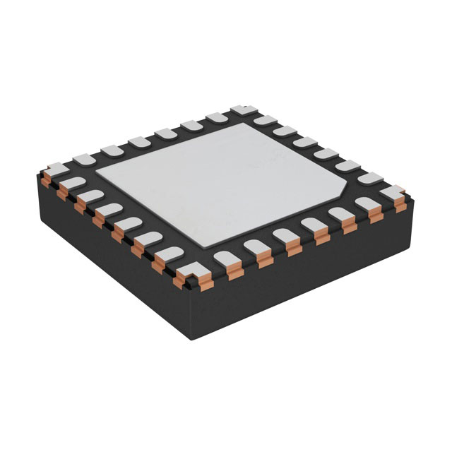
DRV8436E, DRV8436P
DRV8436E,
DRV8436P
SLVSFF0A – JUNE 2020
– REVISED AUGUST
2020
SLVSFF0A – JUNE 2020 – REVISED AUGUST 2020
www.ti.com
DRV8436E/P Dual H-Bridge Motor Drivers With Integrated Current Sense and Smart
Tune Technology
1 Features
•
•
•
•
•
•
•
•
•
•
•
•
•
Dual H-bridge motor driver
– One bipolar stepper motor
– Dual bidirectional brushed-DC motors
– Four unidirectional brushed-DC motors
Integrated current sense functionality
– No sense resistors required
– ±7.5% Full-scale current accuracy
4.5- to 48-V Operating supply voltage range
Multiple control interface options
– PHASE/ENABLE
– PWM
Smart tune decay technology, fixed slow, fast and
mixed decay options
Low RDS(ON): 900 mΩ HS + LS at 24 V, 25°C
High Current Capacity Per Bridge: 2.4-A peak, 1.5A Full-Scale, 1.1-A rms
Configurable Off-Time PWM Chopping
– 7, 16, 24 or 32 μs
Supports 1.8-V, 3.3-V, 5.0-V logic inputs
Low-current sleep mode (2 µA)
Spread spectrum clocking for low electromagnetic
interference (EMI)
Small package and footprint
Protection features
– VM undervoltage lockout (UVLO)
– Charge pump undervoltage (CPUV)
– Overcurrent protection (OCP)
– Thermal shutdown (OTSD)
– Fault condition output (nFAULT)
2 Applications
•
•
•
•
•
•
•
Printers and scanners
ATMs, currency counters, and EPOS
Office and home automation
Factory automation and robotics
Major and small home appliances
IP Network Camera and Video Conferencing
Vacuum, humanoid, and toy robotics
configured as two full H-bridges, charge pump
regulator, current sensing and regulation, and
protection circuitry. The integrated current sensing
uses an internal current mirror architecture, removing
the need for a large power shunt resistor, saving
board area and reducing system cost. A low-power
sleep mode is provided to achieve ultra- low quiescent
current draw by shutting down most of the internal
circuitry. Internal protection features are provided for
supply undervoltage lockout (UVLO), charge pump
undervoltage (CPUV), output overcurrent (OCP), and
device overtemperature (TSD). The DRV8436E/P is
capable of driving up to 1.5-A full scale or 1.1-A rms
output current per H-bridge (dependent on PCB
design).
Device Information
PART NUMBER
PACKAGE (1)
DRV8436EPWPR
HTSSOP (28)
9.7 mm x 4.4 mm
DRV8436ERGER
VQFN (24)
4.0 mm x 4.0 mm
DRV8436PPWPR
HTSSOP (28)
9.7 mm x 4.4 mm
DRV8436PRGER
VQFN (24)
4.0 mm x 4.0 mm
(1)
BODY SIZE (NOM)
For all available packages, see the orderable addendum at
the end of the data sheet.
DRV8436E Simplified Schematic
3 Description
The DRV8436E/P devices are dual H-bridge motor
drivers for a wide variety of industrial applications.
The devices can be used for driving two DC motors,
or a bipolar stepper motor. The output stage of the
driver consists of N-channel power MOSFETs
DRV8436P Simplified Schematic
An©IMPORTANT
NOTICEIncorporated
at the end of this data sheet addresses availability, warranty, changes, use in
safety-critical
applications,
Copyright
2021 Texas Instruments
Submit
Document
Feedback
intellectual property matters and other important disclaimers. PRODUCTION DATA.
Product Folder Links: DRV8436E DRV8436P
1
�DRV8436E, DRV8436P
www.ti.com
SLVSFF0A – JUNE 2020 – REVISED AUGUST 2020
Table of Contents
1 Features............................................................................1
2 Applications..................................................................... 1
3 Description.......................................................................1
4 Revision History.............................................................. 2
5 Pin Configuration and Functions...................................4
Pin Functions.................................................................... 7
6 Specifications.................................................................. 9
6.1 Absolute Maximum Ratings........................................ 9
6.2 ESD Ratings............................................................... 9
6.3 Recommended Operating Conditions.......................10
6.4 Thermal Information..................................................10
6.5 Electrical Characteristics...........................................11
6.6 Typical Characteristics.............................................. 12
7 Detailed Description......................................................13
7.1 Overview................................................................... 13
7.2 Functional Block Diagrams....................................... 14
7.3 Feature Description...................................................16
7.4 Device Functional Modes..........................................27
8 Layout.............................................................................34
8.1 Layout Guidelines..................................................... 34
8.2 Layout Example........................................................ 34
9 Device and Documentation Support............................36
9.1 Device Support......................................................... 36
9.2 Documentation Support............................................ 36
9.3 Related Links............................................................ 36
9.4 Receiving Notification of Documentation Updates....36
9.5 Community Resources..............................................36
9.6 Trademarks............................................................... 36
4 Revision History
NOTE: Page numbers for previous revisions may differ from page numbers in the current version.
Changes from Revision * (June 2020) to Revision A (August 2020)
Page
• Changed device status to "Production Data"......................................................................................................1
2
Submit Document Feedback
Copyright © 2021 Texas Instruments Incorporated
Product Folder Links: DRV8436E DRV8436P
�DRV8436E, DRV8436P
www.ti.com
SLVSFF0A – JUNE 2020 – REVISED AUGUST 2020
Device Options
PART NUMBER
CONTROL INTERFACE
DRV8436E
PHASE/ENABLE
DRV8436P
PWM
Submit Document Feedback
Copyright © 2021 Texas Instruments Incorporated
Product Folder Links: DRV8436E DRV8436P
3
�DRV8436E, DRV8436P
www.ti.com
SLVSFF0A – JUNE 2020 – REVISED AUGUST 2020
5 Pin Configuration and Functions
Figure 5-1. PWP PowerPAD™ Package 28-Pin HTSSOP Top View DRV8436E
4
Submit Document Feedback
Copyright © 2021 Texas Instruments Incorporated
Product Folder Links: DRV8436E DRV8436P
�DRV8436E, DRV8436P
www.ti.com
SLVSFF0A – JUNE 2020 – REVISED AUGUST 2020
Figure 5-2. RGE Package 24-Pin VQFN with Exposed Thermal PAD Top View DRV8436E
Submit Document Feedback
Copyright © 2021 Texas Instruments Incorporated
Product Folder Links: DRV8436E DRV8436P
5
�DRV8436E, DRV8436P
www.ti.com
SLVSFF0A – JUNE 2020 – REVISED AUGUST 2020
Figure 5-3. PWP PowerPAD™ Package 28-Pin HTSSOP Top View DRV8436P
6
Submit Document Feedback
Copyright © 2021 Texas Instruments Incorporated
Product Folder Links: DRV8436E DRV8436P
�DRV8436E, DRV8436P
www.ti.com
SLVSFF0A – JUNE 2020 – REVISED AUGUST 2020
Figure 5-4. RGE Package 24-Pin VQFN with Exposed Thermal PAD Top View DRV8436P
Pin Functions
PIN
PWP
NAME
RGE
TYPE
DESCRIPTION
DRV843
6E
DRV843
DRV8436P
6E
DRV8436P
ADECAY
21
21
16
16
I
Decay mode setting pins. Set the decay mode for bridge A;
quad-level pin.
AEN
25
—
20
—
I
Bridge A enable input. Logic high enables bridge A; logic low
disables the bridge Hi-Z.
AIN1
—
25
—
20
I
Bridge A PWM input. Logic controls the state of H-bridge A;
internal pulldown.
AIN2
—
24
—
19
I
Bridge A PWM input. Logic controls the state of H-bridge A;
internal pulldown.
AOUT1
5
5
3
3
O
Winding A output. Connect to motor winding.
AOUT2
6
6
4
4
O
Winding A output. Connect to motor winding.
APH
24
—
19
—
I
Bridge A phase input. Logic high drives current from AOUT1 to
AOUT2.
VREFA
18
18
13
13
I
Reference voltage input. Voltage on this pin sets the full scale
chopping current in H-bridge A. Maximum value 3.3 V. DVDD
can be used to provide VREF through a resistor divider.
BDECAY
20
20
15
15
I
Decay mode setting pins. Set the decay mode for bridge B;
quad-level pin.
BEN
23
—
18
—
I
Bridge B enable input. Logic high enables bridge B; logic low
disables the bridge Hi-Z.
BIN1
—
23
—
18
I
Bridge B PWM input. Logic controls the state of H-bridge B;
internal pulldown.
BIN2
—
22
—
17
I
Bridge B PWM input. Logic controls the state of H-bridge B;
internal pulldown.
BOUT1
10
10
6
6
O
Winding B output. Connect to motor winding.
Submit Document Feedback
Copyright © 2021 Texas Instruments Incorporated
Product Folder Links: DRV8436E DRV8436P
7
�DRV8436E, DRV8436P
www.ti.com
SLVSFF0A – JUNE 2020 – REVISED AUGUST 2020
PIN
PWP
NAME
TYPE
DESCRIPTION
DRV843
6E
DRV8436P
BOUT2
9
9
5
5
O
Winding B output. Connect to motor winding.
BPH
22
—
17
—
I
Bridge B phase input. Logic high drives current from BOUT1 to
BOUT2.
VREFB
17
17
12
12
I
Reference voltage input. Voltage on this pin sets the full scale
chopping current in H-bridge B. Maximum value 3.3 V. DVDD
can be used to provide VREF through a resistor divider.
CPH
28
28
23
23
CPL
27
27
22
22
PWR
Charge pump switching node. Connect a X7R, 0.022-μF, VMrated ceramic capacitor from CPH to CPL.
GND
14
14
9
9
PWR
Device ground. Connect to system ground.
TOFF
19
19
14
14
I
Sets the decay mode off-time during current chopping; quadlevel pin.
DVDD
15
15
10
10
PWR
Logic supply voltage. Connect a X7R, 0.47-μF, 6.3-V or 10-V
rated ceramic capacitor to GND.
VCP
1
1
24
24
O
Charge pump output. Connect a X7R, 0.22-μF, 16-V ceramic
capacitor to VM.
VM
2, 13
2, 13
1, 8
1, 8
PWR
Power supply. Connect to motor supply voltage and bypass to
GND with two 0.01-μF ceramic capacitors (one for each pin)
plus a bulk capacitor rated for VM.
PGND
3, 12
3, 12
2, 7
2, 7
PWR
Power ground. Both PGND pins are shorted internally. Connect
to system ground on PCB.
nFAULT
16
16
11
11
O
Fault indication. Pulled logic low with fault condition; open-drain
output requires an external pullup resistor.
nSLEEP
26
26
21
21
I
Sleep mode input. Logic high to enable device; logic low to enter
low-power sleep mode; internal pulldown resistor.
4, 7, 8,
11
4, 7, 8, 11
-
-
-
No Connect pins. Leave these pins unconnected.
NC
8
RGE
DRV843
DRV8436P
6E
Submit Document Feedback
Copyright © 2021 Texas Instruments Incorporated
Product Folder Links: DRV8436E DRV8436P
�DRV8436E, DRV8436P
www.ti.com
SLVSFF0A – JUNE 2020 – REVISED AUGUST 2020
6 Specifications
6.1 Absolute Maximum Ratings
over operating free-air temperature range referenced with respect to GND (unless otherwise noted) (1)
Power supply voltage (VM)
MIN
MAX
UNIT
–0.3
50
V
Charge pump voltage (VCP, CPH)
–0.3
VVM + 7
V
Charge pump negative switching pin (CPL)
–0.3
VVM
V
VVM
V
nSLEEP pin voltage (nSLEEP)
–0.3
Internal regulator voltage (DVDD)
–0.3
5.75
V
Control pin voltage (APH, AEN, BPH, BEN, AIN1, AIN2, BIN1, BIN2, nFAULT,
ADECAY, BDECAY, TOFF)
–0.3
5.75
V
0
10
mA
–0.3
5.75
V
Open drain output current (nFAULT)
Reference input pin voltage (VREFA, VREFB)
Continuous phase node pin voltage (AOUT1, AOUT2, BOUT1, BOUT2)
–1
VVM + 1
Transient 100 ns phase node pin voltage (AOUT1, AOUT2, BOUT1, BOUT2)
–3
VVM + 3
Peak drive current (AOUT1, AOUT2, BOUT1, BOUT2)
V
V
Internally Limited
A
Operating ambient temperature, TJ
–40
125
°C
Operating junction temperature, TJ
–40
150
°C
Storage temperature, Tstg
–65
150
°C
(1)
Stresses beyond those listed under Absolute Maximum Ratings may cause permanent damage to the device. These are stress ratings
only, which do not imply functional operation of the device at these or any other conditions beyond those indicated under
Recommended Operating Conditions. Exposure to absolute-maximum-rated conditions for extended periods may affect device
reliability.
6.2 ESD Ratings
VALUE
Human-body model (HBM), per ANSI/ESDA/JEDEC JS-001
V(ESD)
Electrostatic
discharge
Charged-device model (CDM), per JEDEC specification JESD22C101
UNIT
±2000
Corner pins for PWP (1,
14, 15, and 28)
±750
Other pins
±500
Submit Document Feedback
Copyright © 2021 Texas Instruments Incorporated
Product Folder Links: DRV8436E DRV8436P
V
9
�DRV8436E, DRV8436P
www.ti.com
SLVSFF0A – JUNE 2020 – REVISED AUGUST 2020
6.3 Recommended Operating Conditions
over operating free-air temperature range (unless otherwise noted)
MIN
VVM
Supply voltage range for normal (DC) operation
VI
Logic level input voltage
VREF
Reference rms voltage range (VREFA, VREFB)
ƒPWM
Applied PWM signal (APH, AEN, BPH, BEN, AIN1, AIN2, BIN1, BIN2)
MAX
UNIT
4.5
48
V
0
5.3
V
0.05
3.3
V
0
100
kHz
IFS
Motor full-scale current (xOUTx)
0
1.5
A
Irms
Motor RMS current (xOUTx)
0
1.1
A
TA
Operating ambient temperature
–40
125
°C
TJ
Operating junction temperature
–40
150
°C
6.4 Thermal Information
THERMAL METRIC(1)
RθJA
RGE (VQFN)
28 PINS
24 PINS
UNIT
31.3
41.3
°C/W
RθJC(top) Junction-to-case (top) thermal resistance
26.0
32.9
°C/W
RθJB
Junction-to-board thermal resistance
11.5
18.5
°C/W
ψJT
Junction-to-top characterization parameter
0.5
0.6
°C/W
ψJB
Junction-to-board characterization parameter
11.5
18.4
°C/W
RθJC(bot) Junction-to-case (bottom) thermal resistance
3.4
4.8
°C/W
(1)
10
Junction-to-ambient thermal resistance
PWP (HTSSOP)
For more information about traditional and new thermal metrics, see the Semiconductor and IC Package Thermal Metrics application
report.
Submit Document Feedback
Copyright © 2021 Texas Instruments Incorporated
Product Folder Links: DRV8436E DRV8436P
�DRV8436E, DRV8436P
www.ti.com
SLVSFF0A – JUNE 2020 – REVISED AUGUST 2020
6.5 Electrical Characteristics
Typical values are at TA = 25°C and VVM = 24 V. All limits are over recommended operating conditions, unless otherwise
noted.
PARAMETER
TEST CONDITIONS
MIN
TYP
MAX
UNIT
POWER SUPPLIES (VM, DVDD)
IVM
VM operating supply current
nSLEEP = 1, No motor load, IC
Enabled
5
7
mA
IVMQ
VM sleep mode supply current
nSLEEP = 0
2
4
μA
0.6
0.9
ms
0.6
0.9
ms
5
5.5
V
tSLEEP
Sleep time
nSLEEP = 0 to sleep-mode
tWAKE
Wake-up time
nSLEEP = 1 to output transition
tON
Turn-on time
VM > UVLO to output transition
VDVDD
Internal regulator voltage
No external load, 6 V < VVM < 45 V
75
4.5
μs
CHARGE PUMP (VCP, CPH, CPL)
VVCP
VCP operating voltage
f(VCP)
Charge pump switching
frequency
VVM + 5
VVM > UVLO; nSLEEP = 1
V
400
kHz
LOGIC-LEVEL INPUTS (APH, AEN, BPH, BEN, AIN1, AIN2, BIN1, BIN2, nSLEEP)
VIL
Input logic-low voltage
0
VIH
Input logic-high voltage
VHYS
Input logic hysteresis
IIL
Input logic-low current
VIN = 0 V
IIH
Input logic-high current
VIN = 5 V
tPD
Propagation delay
xPH, xEN, xINx input to current change
0.6
1.5
5.5
150
–1
V
V
mV
1
μA
50
μA
850
ns
QUAD-LEVEL INPUTS (ADECAY, BDECAY, TOFF)
VI1
Input logic-low voltage
Tied to GND
VI2
330kΩ ± 5% to GND
0
0.6
V
1
1.25
1.4
V
VI3
Input Hi-Z voltage
Hi-Z (>500kΩ to GND)
1.8
2
2.2
V
VI4
Input logic-high voltage
Tied to DVDD
2.7
IO
Output pull-up current
5.5
10
V
μA
CONTROL OUTPUTS (nFAULT)
VOL
Output logic-low voltage
IO = 5 mA
IOH
Output logic-high leakage
VVM = 24 V
–1
0.4
V
1
μA
MOTOR DRIVER OUTPUTS (AOUT1, AOUT2, BOUT1, BOUT2)
RDS(ON)
RDS(ON)
tSR
High-side FET on resistance
Low-side FET on resistance
Output slew rate
VVM = 24 V, TJ = 25°C, IO = -1 A
450
550
mΩ
VVM = 24 V, TJ = 125°C, IO = -1 A
700
850
mΩ
VVM = 24 V, TJ = 150°C, IO = -1 A
780
950
mΩ
VVM = 24 V, TJ = 25°C, IO = 1 A
450
550
mΩ
VVM = 24 V, TJ = 125°C, IO = 1 A
700
850
mΩ
VVM = 24 V, TJ = 150°C, IO = 1 A
780
950
mΩ
VM = 24V, IO = 0.5 A, Between 10%
and 90%
150
V/µs
2.2
V/A
PWM CURRENT CONTROL (VREFA, VREFB)
KV
tOFF
Transimpedance gain
PWM off-time
TOFF = 0
7
TOFF = 1
16
TOFF = Hi-Z
24
TOFF = 330 kΩ to GND
32
μs
Submit Document Feedback
Copyright © 2021 Texas Instruments Incorporated
Product Folder Links: DRV8436E DRV8436P
11
�DRV8436E, DRV8436P
www.ti.com
SLVSFF0A – JUNE 2020 – REVISED AUGUST 2020
Typical values are at TA = 25°C and VVM = 24 V. All limits are over recommended operating conditions, unless otherwise
noted.
TEST CONDITIONS
MIN
IO = 1.5 A, 10% to 20% current setting
–13
10
IO = 1.5 A, 20% to 67% current setting
–8
8
IO = 1.5 A, 67% to 100% current setting
–7.5
7.5
IO = 1.5 A
–2.5
2.5
VM falling, UVLO falling
4.15
4.25
4.35
VM rising, UVLO rising
4.25
4.35
4.45
PARAMETER
ΔITRIP
Current trip accuracy
IO,CH
AOUT and BOUT current
matching
TYP
MAX
UNIT
%
%
PROTECTION CIRCUITS
VUVLO
VM UVLO lockout
VUVLO,HYS
Undervoltage hysteresis
Rising to falling threshold
VCPUV
Charge pump undervoltage
VCP falling; CPUV report
IOCP
Overcurrent protection
Current through any FET
tOCP
Overcurrent deglitch time
100
V
mV
VVM + 2
V
2.4
A
VM < 37V
3
VM >= 37V
μs
0.5
tRETRY
Overcurrent retry time
TOTSD
Thermal shutdown
Die temperature TJ
4
THYS_OTSD
Thermal shutdown hysteresis
Die temperature TJ
150
165
ms
180
°C
20
°C
6.6 Typical Characteristics
Graph Placeholder
Graph Placeholder
C00
Figure 6-1.
12
C00
Figure 6-2.
Submit Document Feedback
Copyright © 2021 Texas Instruments Incorporated
Product Folder Links: DRV8436E DRV8436P
�DRV8436E, DRV8436P
www.ti.com
SLVSFF0A – JUNE 2020 – REVISED AUGUST 2020
7 Detailed Description
7.1 Overview
The DRV8436E/P are integrated motor driver solutions for bipolar stepper motors or dual brushed-DC motors.
The devices integrate two N-channel power MOSFET H-bridges, integrated current sense and regulation
circuitry. The DRV8436E/P can be powered with a supply voltage between 4.5 and 48 V. The devices are
capable of providing an output current up to 2.4-A peak, 1.5-A full-scale, or 1.1-A root mean square (rms). The
actual full-scale and rms current depends on the ambient temperature, supply voltage, and PCB thermal
capability.
The DRV8436E/P devices use an integrated current-sense architecture which eliminates the need for two
external power sense resistors. This architecture removes the power dissipated in the sense resistors by using a
current mirror approach and using the internal power MOSFETs for current sensing. The current regulation set
point is adjusted by the voltage at the VREFA and VREFB pins. These features reduce external component cost,
board PCB size, and system power consumption.
A simple PH/EN (DRV8436E) or PWM (DRV8436P) interface allows easy interfacing to the controller circuit.
The current regulation is highly configurable, with several decay modes of operation. The decay mode can be
selected as a smart tune Dynamic Decay, fixed slow, mixed, or fast decay. The smart tune decay mode
automatically adjusts the decay setting to minimize current ripple while still reacting quickly to step changes. This
feature greatly simplifies stepper driver integration into a motor drive system. The PWM off-time, tOFF, can be
adjusted to 7, 16, 24, or 32 μs.
A low-power sleep mode is included which allows the system to save power when not driving the motor.
Submit Document Feedback
Copyright © 2021 Texas Instruments Incorporated
Product Folder Links: DRV8436E DRV8436P
13
�DRV8436E, DRV8436P
www.ti.com
SLVSFF0A – JUNE 2020 – REVISED AUGUST 2020
7.2 Functional Block Diagrams
Figure 7-1. DRV8436E Block Diagram
14
Submit Document Feedback
Copyright © 2021 Texas Instruments Incorporated
Product Folder Links: DRV8436E DRV8436P
�DRV8436E, DRV8436P
www.ti.com
SLVSFF0A – JUNE 2020 – REVISED AUGUST 2020
Figure 7-2. DRV8436P Block Diagram
Submit Document Feedback
Copyright © 2021 Texas Instruments Incorporated
Product Folder Links: DRV8436E DRV8436P
15
�DRV8436E, DRV8436P
www.ti.com
SLVSFF0A – JUNE 2020 – REVISED AUGUST 2020
7.3 Feature Description
Table 7-1 shows the recommended values of the external components for the gate driver.
Figure 7-3. Resistor divider connected to the VREF pins
Table 7-1. External Components
16
COMPONENT
PIN 1
PIN 2
CVM1
VM
GND
Two X7R, 0.01-µF, VM-rated ceramic capacitors
RECOMMENDED
CVM2
VM
GND
Bulk, VM-rated capacitor
CVCP
VCP
VM
X7R, 0.22-µF, 16-V ceramic capacitor
CSW
CPH
CPL
X7R, 0.022-µF, VM-rated ceramic capacitor
CDVDD
DVDD
GND
X7R, 0.47-µF to 1-µF, 6.3-V or 10-V rated ceramic capacitor
RnFAULT
VCC
nFAULT
RREF1
VREFx
VCC
RREF2 (Optional)
VREFx
GND
>4.7-kΩ resistor
Resistor to limit chopping current. It is recommended that the value of parallel
combination of RREF1 and RREF2 should be less than 50-kΩ.
Submit Document Feedback
Copyright © 2021 Texas Instruments Incorporated
Product Folder Links: DRV8436E DRV8436P
�DRV8436E, DRV8436P
www.ti.com
SLVSFF0A – JUNE 2020 – REVISED AUGUST 2020
7.3.1 PWM Motor Drivers
The DRV8436E/P contain drivers for two full H-bridges. Figure 7-4 shows a block diagram of the circuitry.
Figure 7-4. PWM Motor Driver Block Diagram
7.3.2 Bridge Control
The DRV8436E is controlled using a PH/EN interface. Table 7-2 gives the full H-bridge state. Note that this table
does not take into account the current control built into the DRV8436E. Positive current is defined in the direction
of xOUT1 to xOUT2.
Table 7-2. DRV8436E (PH/EN) Control Interface
nSLEEP
ENx
PHx
xOUT1
xOUT2
DESCRIPTION
0
X
X
Hi-Z
Hi-Z
Sleep mode; H-bridge disabled Hi-Z
1
0
X
Hi-Z
Hi-Z
H-bridge disabled Hi-Z
1
1
0
L
H
Reverse (current xOUT2 to xOUT1)
1
1
1
H
L
Forward (current xOUT1 to xOUT2)
Submit Document Feedback
Copyright © 2021 Texas Instruments Incorporated
Product Folder Links: DRV8436E DRV8436P
17
�DRV8436E, DRV8436P
www.ti.com
SLVSFF0A – JUNE 2020 – REVISED AUGUST 2020
The DRV8436P is controlled using a PWM interface. Table 7-3 gives the full H-bridge state. Note that this table
does not take into account the current control built into the DRV8436P. Positive current is defined in the direction
of xOUT1 to xOUT2.
Table 7-3. DRV8436P (PWM) Control Interface
nSLEEP
xIN1
xIN2
xOUT1
xOUT2
DESCRIPTION
0
X
X
Hi-Z
Hi-Z
Sleep mode; H-bridge disabled Hi-Z
1
0
0
Hi-Z
Hi-Z
Coast; H-bridge disabled Hi-Z
1
0
1
L
H
Reverse (current xOUT2 to xOUT1)
1
1
0
H
L
Forward (current xOUT1 to xOUT2)
1
1
1
L
L
Brake; low-side slow decay
7.3.3 Current Regulation
The current through the motor windings is regulated by an adjustable, off-time PWM current-regulation circuit.
When an H-bridge is enabled, current rises through the winding at a rate dependent on the DC voltage,
inductance of the winding, and the magnitude of the back EMF present. When the current hits the current
regulation threshold, the bridge enters a decay mode for a period of time determined by the TOFF pin setting to
decrease the current. After the off-time expires, the bridge is re-enabled, starting another PWM cycle.
Table 7-4. Off-Time
Settings
TOFF
OFF-TIME tOFF
0
7 µs
1
16 µs
Hi-Z
24 µs
330kΩ to GND
32 µs
The PWM chopping current is set by a comparator which monitors the voltage across the current sense
MOSFETs in parallel with the low-side power MOSFETs. To generate the reference voltage for the current
chopping comparator, the VREFx input is attenuated by a factor of Kv.
The chopping current (IFS) can be calculated as IFS (A) = VREFx (V) / KV (V/A) = VREFx (V) / 2.2 (V/A).
18
Submit Document Feedback
Copyright © 2021 Texas Instruments Incorporated
Product Folder Links: DRV8436E DRV8436P
�DRV8436E, DRV8436P
www.ti.com
SLVSFF0A – JUNE 2020 – REVISED AUGUST 2020
7.3.4 Decay Modes
During PWM current chopping, the H-bridge is enabled to drive through the motor winding until the PWM current
chopping threshold is reached. This is shown in Figure 7-5, Item 1.
Once the chopping current threshold is reached, the H-bridge can operate in two different states, fast decay or
slow decay. In fast decay mode, once the PWM chopping current level has been reached, the H-bridge reverses
state to allow winding current to flow in a reverse direction. The opposite FETs are turned on; as the winding
current approaches zero, the bridge is disabled to prevent any reverse current flow. Fast decay mode is shown
in Figure 7-5, item 2. In slow decay mode, winding current is re-circulated by enabling both of the low-side FETs
in the bridge. This is shown in Figure 7-5, Item 3.
Figure 7-5. Decay Modes
The decay mode is selected by setting the quad-level ADECAY and BDECAY pins as shown in Table 7-5.
Table 7-5. Decay Mode Settings
xDECAY
DECAY MODE
0
Smart tune Dynamic Decay
330k to GND
Slow decay
Hi-Z
Mixed decay: 30% fast
1
Fast decay
The ADECAY pin sets the decay mode for H-bridge A (AOUT1, AOUT2), and the BDECAY pin sets the decay
mode for H-bridge B (BOUT1, BOUT2).
Submit Document Feedback
Copyright © 2021 Texas Instruments Incorporated
Product Folder Links: DRV8436E DRV8436P
19
�DRV8436E, DRV8436P
www.ti.com
SLVSFF0A – JUNE 2020 – REVISED AUGUST 2020
7.3.4.1 Slow Decay
Increasing Phase Current (A)
ITRIP
tBLANK
tOFF
tBLANK
tOFF
tDRIVE
Decreasing Phase Current (A)
tDRIVE
ITRIP
tBLANK
tDRIVE
tOFF
tBLANK
tDRIVE
tOFF
tBLANK
tDRIVE
Figure 7-6. Slow Decay Mode
During slow decay, both of the low-side FETs of the H-bridge are turned on, allowing the current to be
recirculated.
Slow decay exhibits the least current ripple of the decay modes for a given tOFF. However on decreasing current
steps, slow decay will take a long time to settle to the new ITRIP level because the current decreases very
slowly. If the current at the end of the off time is above the ITRIP level, slow decay will be extended for another
off time duration and so on, till the current at the end of the off time is below ITRIP level.
In cases where current is held for a long time, slow decay may not properly regulate current because no backEMF is present across the motor windings. In this state, motor current can rise very quickly, and may require a
large off-time. In some cases this may cause a loss of current regulation, and a more aggressive decay mode is
recommended.
20
Submit Document Feedback
Copyright © 2021 Texas Instruments Incorporated
Product Folder Links: DRV8436E DRV8436P
�DRV8436E, DRV8436P
www.ti.com
SLVSFF0A – JUNE 2020 – REVISED AUGUST 2020
7.3.4.2 Mixed Decay
Increasing Phase Current (A)
ITRIP
tOFF
tBLANK
tOFF
tBLANK
tDRIVE
Decreasing Phase Current (A)
tDRIVE
tDRIVE
ITRIP
tBLANK
tDRIVE
tFAST
tBLANK
tOFF
tDRIVE
tFAST
tOFF
Figure 7-7. Mixed Decay Mode
Mixed decay begins as fast decay for 30% of tOFF, followed by slow decay for the remainder of tOFF.
This mode exhibits ripple larger than slow decay, but smaller than fast decay. On decreasing current steps,
mixed decay settles to the new ITRIP level faster than slow decay.
Submit Document Feedback
Copyright © 2021 Texas Instruments Incorporated
Product Folder Links: DRV8436E DRV8436P
21
�DRV8436E, DRV8436P
www.ti.com
SLVSFF0A – JUNE 2020 – REVISED AUGUST 2020
7.3.4.3 Fast Decay
Increasing Phase Current (A)
ITRIP
tBLANK
tOFF
tBLANK
tDRIVE
Decreasing Phase Current (A)
tDRIVE
tOFF
tBLANK
tOFF
tDRIVE
ITRIP
tBLANK
tOFF
tDRIVE
tBLANK
tOFF
tDRIVE
tBLANK
tOFF
tDRIVE
Figure 7-8. Fast/Fast Decay Mode
During fast decay, the polarity of the H-bridge is reversed. The H-bridge will be turned off as current approaches
zero in order to prevent current flow in the reverse direction.
Fast decay exhibits the highest current ripple of the decay modes for a given tOFF. Transition time on decreasing
current steps is much faster than slow decay since the current is allowed to decrease much faster.
22
Submit Document Feedback
Copyright © 2021 Texas Instruments Incorporated
Product Folder Links: DRV8436E DRV8436P
�DRV8436E, DRV8436P
www.ti.com
SLVSFF0A – JUNE 2020 – REVISED AUGUST 2020
7.3.4.4 Smart tune Dynamic Decay
The smart tune current regulation scheme is an advanced current-regulation control method compared to
traditional fixed off-time current regulation schemes. Smart tune current regulation scheme helps the stepper
motor driver adjust the decay scheme based on operating factors such as the ones listed as follows:
•
•
•
•
•
Motor winding resistance and inductance
Motor aging effects
Motor dynamic speed and load
Motor supply voltage variation
Low-current versus high-current dI/dt
Increasing Phase Current (A)
ITRIP
tBLANK
tBLANK
tOFF
tBLANK
tOFF
tDRIVE
tDRIVE
tDRIVE
Decreasing Phase Current (A)
ITRIP
tBLANK
tOFF
tBLANK
tDRIVE
tDRIVE
tOFF
tFAST
tBLANK
tDRIVE
tFAST
Figure 7-9. Smart tune Dynamic Decay Mode
Smart tune Dynamic Decay greatly simplifies the decay mode selection by automatically configuring the decay
mode between slow, mixed, and fast decay. In mixed decay, smart tune dynamically adjusts the fast decay
percentage of the total mixed decay time. This feature eliminates motor tuning by automatically determining the
best decay setting that results in the lowest ripple for the motor.
The decay mode setting is optimized iteratively each PWM cycle. If the motor current overshoots the target trip
level, then the decay mode becomes more aggressive (add fast decay percentage) on the next cycle to prevent
regulation loss. If a long drive time must occur to reach the target trip level, the decay mode becomes less
aggressive (remove fast decay percentage) on the next cycle to operate with less ripple and more efficiently. On
falling steps, smart tune Dynamic Decay automatically switches to fast decay to reach the next step quickly.
Smart tune Dynamic Decay is optimal for applications that require minimal current ripple but want to maintain a
fixed frequency in the current regulation scheme.
Submit Document Feedback
Copyright © 2021 Texas Instruments Incorporated
Product Folder Links: DRV8436E DRV8436P
23
�DRV8436E, DRV8436P
www.ti.com
SLVSFF0A – JUNE 2020 – REVISED AUGUST 2020
7.3.4.5 Blanking time
After the current is enabled (start of drive phase) in an H-bridge, the current sense comparator is ignored for a
period of time (tBLANK) before enabling the current-sense circuitry. The blanking time also sets the minimum drive
time of the PWM. The blanking time is approximately 860ns.
7.3.5 Charge Pump
A charge pump is integrated to supply a high-side N-channel MOSFET gate-drive voltage. The charge pump
requires a capacitor between the VM and VCP pins to act as the storage capacitor. Additionally a ceramic
capacitor is required between the CPH and CPL pins to act as the flying capacitor.
Figure 7-10. Charge Pump Block Diagram
24
Submit Document Feedback
Copyright © 2021 Texas Instruments Incorporated
Product Folder Links: DRV8436E DRV8436P
�DRV8436E, DRV8436P
www.ti.com
SLVSFF0A – JUNE 2020 – REVISED AUGUST 2020
7.3.6 Linear Voltage Regulators
A linear voltage regulator is integrated in the device. The DVDD regulator can be used to provide a reference
voltage. DVDD can supply a maximum of 2 mA load. For proper operation, bypass the DVDD pin to GND using
a ceramic capacitor.
The DVDD output is nominally 5-V. When the DVDD LDO current load exceeds 2 mA, the output voltage drops
significantly.
Figure 7-11. Linear Voltage Regulator Block Diagram
If a digital input must be tied permanently high (that is, ADECAY, BDECAY or TOFF), tying the input to the DVDD
pin instead of an external regulator is preferred. This method saves power when the VM pin is not applied or in
sleep mode: the DVDD regulator is disabled and current does not flow through the input pulldown resistors. For
reference, logic level inputs have a typical pulldown of 200 kΩ.
The nSLEEP pin cannot be tied to DVDD, else the device will never exit sleep mode.
Submit Document Feedback
Copyright © 2021 Texas Instruments Incorporated
Product Folder Links: DRV8436E DRV8436P
25
�DRV8436E, DRV8436P
www.ti.com
SLVSFF0A – JUNE 2020 – REVISED AUGUST 2020
7.3.7 Logic and Quad-Level Pin Diagrams
Figure 7-12 gives the input structure for logic-level pins APH, AEN, BPH, BEN, AIN1, AIN2, BIN1, BIN2 and
nSLEEP:
Figure 7-12. Logic-level Input Pin Diagram
Quad-level logic pins TOFF, ADECAY, and BDECAY have the following structure as shown in Figure 7-13.
Figure 7-13. Quad-Level Input Pin Diagram
7.3.7.1 nFAULT Pin
The nFAULT pin has an open-drain output and should be pulled up to a 5-V or 3.3-V supply. When a fault is
detected, the nFAULT pin will be logic low. nFAULT pin will be high after power-up. For a 5-V pullup, the nFAULT
pin can be tied to the DVDD pin with a resistor. For a 3.3-V pullup, an external 3.3-V supply must be used.
Output
nFAULT
Figure 7-14. nFAULT Pin
7.3.8 Protection Circuits
The devices are fully protected against supply undervoltage, charge pump undervoltage, output overcurrent, and
device overtemperature events.
7.3.8.1 VM Undervoltage Lockout (UVLO)
If at any time the voltage on the VM pin falls below the UVLO-threshold voltage for the voltage supply, all the
outputs are disabled, and the nFAULT pin is driven low. The charge pump is disabled in this condition. Normal
26
Submit Document Feedback
Copyright © 2021 Texas Instruments Incorporated
Product Folder Links: DRV8436E DRV8436P
�DRV8436E, DRV8436P
www.ti.com
SLVSFF0A – JUNE 2020 – REVISED AUGUST 2020
operation resumes (motor-driver operation and nFAULT released) when the VM undervoltage condition is
removed.
7.3.8.2 VCP Undervoltage Lockout (CPUV)
If at any time the voltage on the VCP pin falls below the CPUV voltage, all the outputs are disabled, and the
nFAULT pin is driven low. The charge pump remains active during this condition. Normal operation resumes
(motor-driver operation and nFAULT released) when the VCP undervoltage condition is removed.
7.3.8.3 Overcurrent Protection (OCP)
An analog current-limit circuit on each FET limits the current through the FET by removing the gate drive. If this
current limit persists for longer than the tOCP time, the FETs in that particular H-bridge are disabled and the
nFAULT pin is driven low. The charge pump remains active during this condition. Normal operation resumes
automatically (motor-driver operation starts and nFAULT released) after the tRETRY time has elapsed and the
fault condition is removed.
7.3.8.4 Thermal Shutdown (OTSD)
If the die temperature exceeds the thermal shutdown limit (TOTSD) all MOSFETs in the H-bridge are disabled,
and the nFAULT pin is driven low. The charge pump remains active during this condition. Normal operation
resumes (motor-driver operation and the nFAULT line released) when the junction temperature falls below the
overtemperature threshold limit minus the hysteresis (TOTSD – THYS_OTSD).
7.3.8.5
Table 7-6. Fault Condition Summary
FAULT
CONDITION
ERROR
REPORT
H-BRIDGE
CHARGE
PUMP
INDEXER
LOGIC
RECOVERY
VM undervoltage
(UVLO)
VM < VUVLO
nFAULT
Disabled
Disabled
Disabled
Reset
(VDVDD < 3.9
V)
Automatic: VM >
VUVLO
VCP undervoltage
(CPUV)
VCP < VCPUV
nFAULT
Disabled
Operating
Operating
Operating
VCP > VCPUV
Overcurrent (OCP)
IOUT > IOCP
nFAULT
Disabled
Operating
Operating
Operating
Automatic retry:
tRETRY
Thermal Shutdown
(OTSD)
TJ > TTSD
nFAULT
Disabled
Disabled
Operating
Operating
Automatic: TJ < TOTSD
- THYS_OTSD
7.4 Device Functional Modes
7.4.1 Sleep Mode (nSLEEP = 0)
The state of the device is managed by the nSLEEP pin. When the nSLEEP pin is low, the device enters a lowpower sleep mode. In sleep mode, all the internal MOSFETs are disabled and the charge pump is disabled. The
tSLEEP time must elapse after a falling edge on the nSLEEP pin before the device enters sleep mode. The device
is brought out of sleep automatically if the nSLEEP pin is brought high. The tWAKE time must elapse before the
device is ready for inputs.
7.4.2 Operating Mode (nSLEEP = 1)
When the nSLEEP pin is high, and VM > UVLO, the device enters the active mode. The tWAKE time must elapse
before the device is ready for inputs.
7.4.3 Functional Modes Summary
Table 7-7 lists a summary of the functional modes.
Table 7-7. Functional Modes Summary
CONDITION
Sleep mode
CONFIGURATI
ON
4.5 V < VM < 48 V
nSLEEP pin = 0
H-BRIDGE
Disabled
DVDD Regulator CHARGE PUMP
Disbaled
Disabled
Logic
Disabled
Submit Document Feedback
Copyright © 2021 Texas Instruments Incorporated
Product Folder Links: DRV8436E DRV8436P
27
�DRV8436E, DRV8436P
www.ti.com
SLVSFF0A – JUNE 2020 – REVISED AUGUST 2020
Table 7-7. Functional Modes Summary (continued)
CONDITION
Operating
28
CONFIGURATI
ON
4.5 V < VM < 48 V
nSLEEP pin = 1
H-BRIDGE
Operating
DVDD Regulator CHARGE PUMP
Operating
Submit Document Feedback
Operating
Logic
Operating
Copyright © 2021 Texas Instruments Incorporated
Product Folder Links: DRV8436E DRV8436P
�DRV8436E, DRV8436P
www.ti.com
SLVSFF0A – JUNE 2020 – REVISED AUGUST 2020
Application and Implementation
Note
Information in the following applications sections is not part of the TI component specification, and TI
does not warrant its accuracy or completeness. TI’s customers are responsible for determining
suitability of components for their purposes. Customers should validate and test their design
implementation to confirm system functionality.
8.1 Application Information
The DRV8436E/P is used in stepper or brushed motor control.
8.2 Typical Application
The following design procedure can be used to configure the DRV8436E/P. In this application, the device will be
used to drive a stepper motor.
Figure 8-1. Typical Application Schematic
8.2.1 Design Requirements
Table 8-1 lists the design input parameters for system design.
Submit Document Feedback
Copyright © 2021 Texas Instruments Incorporated
Product Folder Links: DRV8436E DRV8436P
29
�DRV8436E, DRV8436P
www.ti.com
SLVSFF0A – JUNE 2020 – REVISED AUGUST 2020
Table 8-1. Design Parameters
DESIGN PARAMETER
REFERENCE
EXAMPLE VALUE
Supply voltage
VM
Motor winding resistance
RL
4.5 Ω/phase
Motor winding inductance
LL
10.5 mH/phase
Motor full step angle
Target microstepping level
Target motor speed
Target full-scale current
24 V
θstep
1.8°/step
nm
Non-circular 1/2 step
v
120 rpm
IFS
800 mA
8.2.2 Detailed Design Procedure
8.2.2.1 Current Regulation
In a stepper motor, the full-scale current (IFS) is the maximum current driven through either winding. This quantity
depends on the VREFx voltage. The maximum allowable voltage on the VREFx pins is 3.3 V. DVDD can be
used to provide VREFx through a resistor divider.
IFS (A) = VREF (V) / 2.2 (V/A)
Note
The IFS current must also follow the equation shown below to avoid saturating the motor. VM is the
motor supply voltage, and RL is the motor winding resistance.
IFS (A)
VM (V)
2 u RDS(ON) (:)
RL (:)
(1)
8.2.2.2 Stepper Motor Speed
Next, the driving waveform needs to be planned. In order to command the correct speed, determine the
frequency of the input waveform.
If the target motor speed is too high, the motor will not spin. Make sure that the motor can support the target
speed.
For a desired motor speed (v), microstepping level (nm), and motor full step angle (θstep),
v (rpm) u 360 (q / rot)
Tstep (q / step) u nm (steps / microstep) u 60 (s / min)
¦step VWHSV V
(2)
θstep can be found in the stepper motor data sheet or written on the motor itself.
The frequency ƒstep gives the frequency of input change on the device. For the design parameters mentioned
above, fstep can be calculated as 800 Hz.
¦step VWHSV V
120 rpm u 360q / rot
1.8q / step u 1/ 2 steps / microstep u 60 s / min
+]
(3)
8.2.2.3 Decay Modes
The device supports several different decay modes: slow decay, fast decay, mixed decay, and smart tune. The
current through the motor windings is regulated using an adjustable fixed-time-off scheme. This means that after
any drive phase, when a motor winding current has hit the current chopping threshold (ITRIP), the device will
place the winding in one of the decay modes for TOFF. After TOFF, a new drive phase starts.
30
Submit Document Feedback
Copyright © 2021 Texas Instruments Incorporated
Product Folder Links: DRV8436E DRV8436P
�DRV8436E, DRV8436P
www.ti.com
SLVSFF0A – JUNE 2020 – REVISED AUGUST 2020
8.3 Alternate Application
In this application, the device is configured to drive bidirectional currents through two external loads (such as two
brushed DC motors) using H-bridge configuration. The H-bridge polarity and duty cycle are controlled from the
external controller to the xEN/xIN1 and xPH/xIN2 pins.
Figure 8-2. Typical Application Schematic
8.3.1 Design Requirements
Table 8-2 gives design input parameters for system design.
Table 8-2. Design Parameters
DESIGN PARAMETER
REFERENCE
EXAMPLE VALUE
Supply voltage
VM
24 V
Motor winding resistance
RL
6Ω
Motor winding inductance
fPWM
Target maximum motor current
LL
4.1 mH
Switching frequency
20 kHz
ITRIP
1A
Submit Document Feedback
Copyright © 2021 Texas Instruments Incorporated
Product Folder Links: DRV8436E DRV8436P
31
�DRV8436E, DRV8436P
www.ti.com
SLVSFF0A – JUNE 2020 – REVISED AUGUST 2020
8.3.2 Detailed Design Procedure
8.3.2.1 Current Regulation
The maximum current (ITRIP) is set by the VREFx analog voltage. When starting a brushed-DC motor, a large
inrush current may occur because there is no back-EMF. Current regulation will act to limit this inrush current
and prevent high current on startup.
32
Submit Document Feedback
Copyright © 2021 Texas Instruments Incorporated
Product Folder Links: DRV8436E DRV8436P
�DRV8436E, DRV8436P
www.ti.com
SLVSFF0A – JUNE 2020 – REVISED AUGUST 2020
Power Supply Recommendations
The device is designed to operate from an input voltage supply (VM) range from 4.5 V to 48 V. A 0.01-µF
ceramic capacitor rated for VM must be placed at each VM pin as close to the device as possible. In addition, a
bulk capacitor must be included on VM.
8.1 Bulk Capacitance
Having appropriate local bulk capacitance is an important factor in motor drive system design. It is generally
beneficial to have more bulk capacitance, while the disadvantages are increased cost and physical size.
The amount of local capacitance needed depends on a variety of factors, including:
•
•
•
•
•
•
The highest current required by the motor system
The power supply’s capacitance and ability to source current
The amount of parasitic inductance between the power supply and motor system
The acceptable voltage ripple
The type of motor used (brushed DC, brushless DC, stepper)
The motor braking method
The inductance between the power supply and motor drive system will limit the rate current can change from the
power supply. If the local bulk capacitance is too small, the system will respond to excessive current demands or
dumps from the motor with a change in voltage. When adequate bulk capacitance is used, the motor voltage
remains stable and high current can be quickly supplied.
The data sheet generally provides a recommended value, but system-level testing is required to determine the
appropriate sized bulk capacitor.
The voltage rating for bulk capacitors should be higher than the operating voltage, to provide margin for cases
when the motor transfers energy to the supply.
Power Supply
Parasitic Wire
Inductance
Motor Drive System
VM
+
±
+
Motor
Driver
GND
Local
Bulk Capacitor
IC Bypass
Capacitor
Copyright © 2016, Texas Instruments Incorporated
Figure 8-1. Example Setup of Motor Drive System With External Power Supply
Submit Document Feedback
Copyright © 2021 Texas Instruments Incorporated
Product Folder Links: DRV8436E DRV8436P
33
�DRV8436E, DRV8436P
www.ti.com
SLVSFF0A – JUNE 2020 – REVISED AUGUST 2020
8 Layout
8.1 Layout Guidelines
The VM pin should be bypassed to GND using a low-ESR ceramic bypass capacitor with a recommended value
of 0.01 µF rated for VM. This capacitor should be placed as close to the VM pin as possible with a thick trace or
ground plane connection to the device GND pin.
The VM pin must be bypassed to ground using a bulk capacitor rated for VM. This component can be an
electrolytic capacitor.
A low-ESR ceramic capacitor must be placed in between the CPL and CPH pins. A value of 0.022 µF rated for
VM is recommended. Place this component as close to the pins as possible.
A low-ESR ceramic capacitor must be placed in between the VM and VCP pins. A value of 0.22 µF rated for 16
V is recommended. Place this component as close to the pins as possible.
Bypass the DVDD pin to ground with a low-ESR ceramic capacitor. A value of 0.47 µF rated for 6.3 V is
recommended. Place this bypassing capacitor as close to the pin as possible.
The thermal PAD must be connected to system ground.
8.2 Layout Example
Figure 8-1. HTSSOP Layout Recommendation
34
Submit Document Feedback
Copyright © 2021 Texas Instruments Incorporated
Product Folder Links: DRV8436E DRV8436P
�DRV8436E, DRV8436P
www.ti.com
SLVSFF0A – JUNE 2020 – REVISED AUGUST 2020
Figure 8-2. QFN Layout Recommendation
Submit Document Feedback
Copyright © 2021 Texas Instruments Incorporated
Product Folder Links: DRV8436E DRV8436P
35
�DRV8436E, DRV8436P
www.ti.com
SLVSFF0A – JUNE 2020 – REVISED AUGUST 2020
9 Device and Documentation Support
9.1 Device Support
9.1.1 Development Support
9.1.2 Device Nomenclature
9.2 Documentation Support
9.2.1 Related Documentation
For related documentation see the following:
• Texas Instruments, PowerPAD™ Thermally Enhanced Package application report
• Texas Instruments, PowerPAD™ Made Easy application report
• Texas Instruments, Current Recirculation and Decay Modes application report
• Texas Instruments, Calculating Motor Driver Power Dissipation application report
• Texas Instruments, Understanding Motor Driver Current Ratings application report
• Texas Instruments, High Resolution Microstepping Driver With the DRV88xx Series application report
9.3 Related Links
The table below lists quick access links. Categories include technical documents, support and community
resources, tools and software, and quick access to order now.
9.4 Receiving Notification of Documentation Updates
To receive notification of documentation updates, navigate to the device product folder on ti.com. In the upper
right corner, click on Alert me to register and receive a weekly digest of any product information that has
changed. For change details, review the revision history included in any revised document.
9.5 Community Resources
9.6 Trademarks
All trademarks are the property of their respective owners.
36
Submit Document Feedback
Copyright © 2021 Texas Instruments Incorporated
Product Folder Links: DRV8436E DRV8436P
�DRV8436E, DRV8436P
www.ti.com
SLVSFF0A – JUNE 2020 – REVISED AUGUST 2020
Mechanical, Packaging, and Orderable Information
The following pages include mechanical, packaging, and orderable information. This information is the most
current data available for the designated devices. This data is subject to change without notice and revision of
this document. For browser-based versions of this data sheet, refer to the left-hand navigation.
Submit Document Feedback
Copyright © 2021 Texas Instruments Incorporated
Product Folder Links: DRV8436E DRV8436P
37
�DRV8436E, DRV8436P
www.ti.com
SLVSFF0A – JUNE 2020 – REVISED AUGUST 2020
PACKAGE OUTLINE
RGE0024B
VQFN - 1 mm max height
SCALE 3.000
PLASTIC QUAD FLATPACK - NO LEAD
4.1
3.9
A
B
0.5
0.3
PIN 1 INDEX AREA
4.1
3.9
0.3
0.2
DETAIL
OPTIONAL TERMINAL
TYPICAL
C
1 MAX
SEATING PLANE
0.05
0.00
0.08 C
2X 2.5
(0.2) TYP
2.45 0.1
7
SEE TERMINAL
DETAIL
12
EXPOSED
THERMAL PAD
13
6
2X
2.5
SYMM
25
18
1
20X 0.5
24
PIN 1 ID
(OPTIONAL)
0.3
0.2
0.1
C A B
0.05
24X
19
SYMM
24X
0.5
0.3
4219013/A 05/2017
NOTES:
1. All linear dimensions are in millimeters. Any dimensions in parenthesis are for reference only. Dimensioning and tolerancing
per ASME Y14.5M.
2. This drawing is subject to change without notice.
3. The package thermal pad must be soldered to the printed circuit board for thermal and mechanical performance.
www.ti.com
38
Submit Document Feedback
Copyright © 2021 Texas Instruments Incorporated
Product Folder Links: DRV8436E DRV8436P
�DRV8436E, DRV8436P
www.ti.com
SLVSFF0A – JUNE 2020 – REVISED AUGUST 2020
EXAMPLE BOARD LAYOUT
RGE0024B
VQFN - 1 mm max height
PLASTIC QUAD FLATPACK - NO LEAD
( 2.45)
SYMM
24
19
24X (0.6)
1
18
24X (0.25)
(R0.05)
TYP
25
SYMM
(3.8)
20X (0.5)
13
6
( 0.2) TYP
VIA
12
7
(0.975) TYP
(3.8)
LAND PATTERN EXAMPLE
EXPOSED METAL SHOWN
SCALE:15X
0.07 MIN
ALL AROUND
0.07 MAX
ALL AROUND
SOLDER MASK
OPENING
METAL
EXPOSED
METAL
SOLDER MASK
OPENING
EXPOSED
METAL
NON SOLDER MASK
DEFINED
(PREFERRED)
METAL UNDER
SOLDER MASK
SOLDER MASK
DEFINED
SOLDER MASK DETAILS
4219013/A 05/2017
NOTES: (continued)
4. This package is designed to be soldered to a thermal pad on the board. For more information, see Texas Instruments literature
number SLUA271 (www.ti.com/lit/slua271).
5. Vias are optional depending on application, refer to device data sheet. If any vias are implemented, refer to their locations shown
on this view. It is recommended that vias under paste be filled, plugged or tented.
www.ti.com
Submit Document Feedback
Copyright © 2021 Texas Instruments Incorporated
Product Folder Links: DRV8436E DRV8436P
39
�DRV8436E, DRV8436P
www.ti.com
SLVSFF0A – JUNE 2020 – REVISED AUGUST 2020
EXAMPLE STENCIL DESIGN
RGE0024B
VQFN - 1 mm max height
PLASTIC QUAD FLATPACK - NO LEAD
4X ( 1.08)
(0.64) TYP
24
19
24X (0.6)
1
25
18
24X (0.25)
(R0.05) TYP
(0.64)
TYP
SYMM
(3.8)
20X (0.5)
13
6
METAL
TYP
12
7
SYMM
(3.8)
SOLDER PASTE EXAMPLE
BASED ON 0.125 mm THICK STENCIL
EXPOSED PAD 25
78% PRINTED SOLDER COVERAGE BY AREA UNDER PACKAGE
SCALE:20X
4219013/A 05/2017
NOTES: (continued)
6. Laser cutting apertures with trapezoidal walls and rounded corners may offer better paste release. IPC-7525 may have alternate
design recommendations.
www.ti.com
40
Submit Document Feedback
Copyright © 2021 Texas Instruments Incorporated
Product Folder Links: DRV8436E DRV8436P
�DRV8436E, DRV8436P
www.ti.com
SLVSFF0A – JUNE 2020 – REVISED AUGUST 2020
PACKAGE OUTLINE
PWP0028P
TM
PowerPAD TSSOP - 1.2 mm max height
SCALE 2.000
SMALL OUTLINE PACKAGE
C
6.6
TYP
6.2
A
0.1 C
PIN 1 INDEX
AREA
SEATING
PLANE
26X 0.65
28
1
2X
9.8
9.6
NOTE 3
8.45
14
15
0.30
0.19
0.1
C A B
28X
4.5
4.3
B
SEE DETAIL A
(0.15) TYP
2X 0.8 MAX
NOTE 5
14
15
2X 0.805 MAX
NOTE 5
0.25
GAGE PLANE
1.2 MAX
6.46
5.38
THERMAL
PAD
0.15
0.05
0.75
0.50
0 -8
DETAIL A
A 20
TYPICAL
28
1
2.34
1.61
4224756/A 01/2019
PowerPAD is a trademark of Texas Instruments.
NOTES:
1. All linear dimensions are in millimeters. Any dimensions in parenthesis are for reference only. Dimensioning and tolerancing
per ASME Y14.5M.
2. This drawing is subject to change without notice.
3. This dimension does not include mold flash, protrusions, or gate burrs. Mold flash, protrusions, or gate burrs shall not
exceed 0.15 mm per side.
4. Reference JEDEC registration MO-153.
5. Features may differ or may not be present.
www.ti.com
Submit Document Feedback
Copyright © 2021 Texas Instruments Incorporated
Product Folder Links: DRV8436E DRV8436P
41
�DRV8436E, DRV8436P
www.ti.com
SLVSFF0A – JUNE 2020 – REVISED AUGUST 2020
EXAMPLE BOARD LAYOUT
PWP0028P
TM
PowerPAD TSSOP - 1.2 mm max height
SMALL OUTLINE PACKAGE
(3.4)
NOTE 9
(2.34)
METAL COVERED
BY SOLDER MASK
SYMM
28X (1.5)
1
28X (0.45)
28
SEE DETAILS
(R0.05) TYP
(6.46)
26X (0.65)
(0.6)
SYMM
(9.7)
NOTE 9
SOLDER MASK
DEFINED PAD
(1.2) TYP
( 0.2) TYP
VIA
15
14
(1.3) TYP
(5.8)
LAND PATTERN EXAMPLE
EXPOSED METAL SHOWN
SCALE: 8X
SOLDER MASK
OPENING
SOLDER MASK
OPENING
METAL UNDER
SOLDER MASK
METAL
EXPOSED METAL
EXPOSED METAL
0.05 MIN
ALL AROUND
0.05 MAX
ALL AROUND
NON-SOLDER MASK
DEFINED
(PREFERRED)
SOLDER MASK
DEFINED
SOLDER MASK DETAILS
15.000
4224756/A 01/2019
NOTES: (continued)
6. Publication IPC-7351 may have alternate designs.
7. Solder mask tolerances between and around signal pads can vary based on board fabrication site.
8. This package is designed to be soldered to a thermal pad on the board. For more information, see Texas Instruments literature
numbers SLMA002 (www.ti.com/lit/slma002) and SLMA004 (www.ti.com/lit/slma004).
9. Size of metal pad may vary due to creepage requirement.
10. Vias are optional depending on application, refer to device data sheet. It is recommended that vias under paste be filled, plugged
or tented.
www.ti.com
42
Submit Document Feedback
Copyright © 2021 Texas Instruments Incorporated
Product Folder Links: DRV8436E DRV8436P
�DRV8436E, DRV8436P
www.ti.com
SLVSFF0A – JUNE 2020 – REVISED AUGUST 2020
EXAMPLE STENCIL DESIGN
PWP0028P
TM
PowerPAD TSSOP - 1.2 mm max height
SMALL OUTLINE PACKAGE
(2.34)
BASED ON
0.125 THICK
STENCIL
28X (1.5)
METAL COVERED
BY SOLDER MASK
1
28
28X (0.45)
(R0.05) TYP
26X (0.65)
(6.46)
BASED ON
0.125 THICK
STENCIL
SYMM
15
14
SYMM
(5.8)
SEE TABLE FOR
DIFFERENT OPENINGS
FOR OTHER STENCIL
THICKNESSES
SOLDER PASTE EXAMPLE
BASED ON 0.125 mm THICK STENCIL
SCALE: 8X
STENCIL
THICKNESS
SOLDER STENCIL
OPENING
0.1
0.125
0.15
0.175
2.62 X 7.22
2.34 X 6.46 (SHOWN)
2.14 X 5.90
1.98 X 5.46
4224756/A 01/2019
NOTES: (continued)
11. Laser cutting apertures with trapezoidal walls and rounded corners may offer better paste release. IPC-7525 may have alternate
design recommendations.
12. Board assembly site may have different recommendations for stencil design.
www.ti.com
Submit Document Feedback
Copyright © 2021 Texas Instruments Incorporated
Product Folder Links: DRV8436E DRV8436P
43
�PACKAGE OPTION ADDENDUM
www.ti.com
27-Aug-2021
PACKAGING INFORMATION
Orderable Device
Status
(1)
Package Type Package Pins Package
Drawing
Qty
Eco Plan
(2)
Lead finish/
Ball material
MSL Peak Temp
Op Temp (°C)
Device Marking
(3)
(4/5)
(6)
DRV8436EPWPR
ACTIVE
HTSSOP
PWP
28
2500
RoHS & Green
NIPDAU
Level-3-260C-168 HR
-40 to 125
DRV8436E
DRV8436ERGER
ACTIVE
VQFN
RGE
24
3000
RoHS & Green
NIPDAU
Level-1-260C-UNLIM
-40 to 125
DRV
8436E
DRV8436PPWPR
ACTIVE
HTSSOP
PWP
28
2500
RoHS & Green
NIPDAU
Level-3-260C-168 HR
-40 to 125
DRV8436P
DRV8436PRGER
ACTIVE
VQFN
RGE
24
3000
RoHS & Green
NIPDAU
Level-1-260C-UNLIM
-40 to 125
DRV
8436P
(1)
The marketing status values are defined as follows:
ACTIVE: Product device recommended for new designs.
LIFEBUY: TI has announced that the device will be discontinued, and a lifetime-buy period is in effect.
NRND: Not recommended for new designs. Device is in production to support existing customers, but TI does not recommend using this part in a new design.
PREVIEW: Device has been announced but is not in production. Samples may or may not be available.
OBSOLETE: TI has discontinued the production of the device.
(2)
RoHS: TI defines "RoHS" to mean semiconductor products that are compliant with the current EU RoHS requirements for all 10 RoHS substances, including the requirement that RoHS substance
do not exceed 0.1% by weight in homogeneous materials. Where designed to be soldered at high temperatures, "RoHS" products are suitable for use in specified lead-free processes. TI may
reference these types of products as "Pb-Free".
RoHS Exempt: TI defines "RoHS Exempt" to mean products that contain lead but are compliant with EU RoHS pursuant to a specific EU RoHS exemption.
Green: TI defines "Green" to mean the content of Chlorine (Cl) and Bromine (Br) based flame retardants meet JS709B low halogen requirements of