Product
Folder
Sample &
Buy
Support &
Community
Tools &
Software
Technical
Documents
DRV8601
SLOS629D – JULY 2010 – REVISED OCTOBER 2016
DRV8601 Haptic Driver for DC Motors (ERMs) and Linear Vibrators (LRAs)
With Ultra-Fast Turnon
1 Features
3 Description
•
•
The DRV8601 is a single-supply haptic driver that is
optimized to drive a DC motor (also known as
Eccentric Rotating Mass or ERM in haptics
terminology) or a linear vibrator (also known as
Linear Resonant Actuator or LRA in haptics
terminology) using a single-ended PWM input signal.
With a fast turn-on time of 100 µs, the DRV8601 is an
excellent haptic driver for use in mobile phones and
other portable electronic devices.
1
•
•
•
•
•
•
•
High Current Output: 400 mA
Wide Supply Voltage Range (2.5 V to 5.5 V) for
Direct Battery Operation
Low Quiescent Current: 1.7 mA (Typical)
Fast Startup Time: 100 µs
Low Shutdown Current: 10 nA
Output Short-Circuit Protection
Thermal Protection
Enable Pin is 1.8-V Compatible
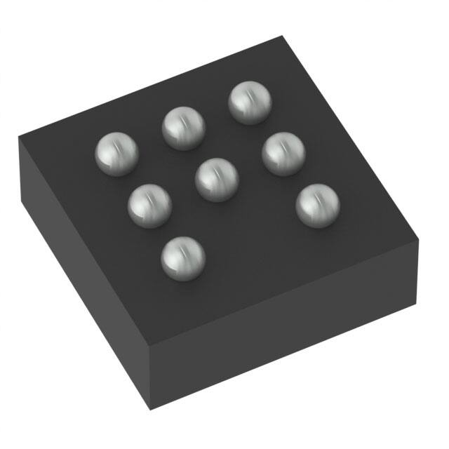
Available in a 3-mm x 3-mm VQFN Package
(DRB) and 2-mm x 2-mm MicroStar Junior™
PBGA Package (ZQV)
The DRV8601 drives up to 400 mA from a
3.3-V supply. Near rail-to-rail output swing under load
ensures sufficient voltage drive for most DC motors.
Differential output drive allows the polarity of the
voltage across the output to be reversed quickly,
thereby enabling motor speed control in both
clockwise and counter-clockwise directions, allowing
quick motor stopping. A wide input voltage range
allows precise speed control of both DC motors and
linear vibrators.
2 Applications
•
•
•
•
•
Mobile Phones
Tablets
Portable Gaming Consoles
Portable Navigation Devices
Appliance Consoles
With a typical quiescent current of 1.7 mA and a
shutdown current of 10 nA, the DRV8601 is ideal for
portable applications. The DRV8601 has thermal and
output short-circuit protection to prevent the device
from being damaged during fault conditions.
Device Information(1)
PART NUMBER
DRV8601
PACKAGE
BODY SIZE (NOM)
DRB (8)
3.00 mm × 3.00 mm
ZQV (8)
2.00 mm × 2.00 mm
(1) For all available packages, see the orderable addendum at
the end of the datasheet.
spacer
Block Diagram
Application
Processor
OUTC
IN1
REFOUT
PWM2
IN2
OUT+
GPIO
EN
VDD
M
LRA or
ERM
2.5 V ± 5.5 V
C(VDD)
GND
DRV8601
Copyright © 2016, Texas Instruments Incorporated
1
An IMPORTANT NOTICE at the end of this data sheet addresses availability, warranty, changes, use in safety-critical applications,
intellectual property matters and other important disclaimers. PRODUCTION DATA.
�DRV8601
SLOS629D – JULY 2010 – REVISED OCTOBER 2016
www.ti.com
Table of Contents
1
2
3
4
5
6
7
Features ..................................................................
Applications ...........................................................
Description .............................................................
Revision History.....................................................
Pin Configuration and Functions .........................
Specifications.........................................................
1
1
1
2
3
4
6.1
6.2
6.3
6.4
6.5
6.6
6.7
4
4
4
4
5
5
5
Absolute Maximum Ratings ......................................
ESD Ratings ............................................................
Recommended Operating Conditions.......................
Thermal Information .................................................
Electrical Characteristics...........................................
Operating Characteristics..........................................
Typical Characteristics ..............................................
Detailed Description .............................................. 8
7.1 Overview ................................................................... 8
7.2 Functional Block Diagram ......................................... 8
7.3 Feature Description................................................... 8
7.4 Device Functional Modes.......................................... 9
8
Application and Implementation ........................ 10
8.1 Application Information............................................ 10
8.2 Typical Applications ............................................... 11
9 Power Supply Recommendations...................... 15
10 Layout................................................................... 16
10.1 Layout Guidelines ................................................. 16
10.2 Layout Example .................................................... 16
11 Device and Documentation Support ................. 17
11.1
11.2
11.3
11.4
11.5
Receiving Notification of Documentation Updates
Community Resources..........................................
Trademarks ...........................................................
Electrostatic Discharge Caution ............................
Glossary ................................................................
17
17
17
17
17
12 Mechanical, Packaging, and Orderable
Information ........................................................... 17
4 Revision History
NOTE: Page numbers for previous revisions may differ from page numbers in the current version.
Changes from Revision C (January 2016) to Revision D
Page
•
Added the ZQV package to the Features list and the Device Information table .................................................................... 1
•
Added the ZQV pinout to the Pin Configuration and Functions section................................................................................. 3
•
Added ZQV values to the Thermal Information table ............................................................................................................. 4
•
Added Figure 20 .................................................................................................................................................................. 16
Changes from Revision B (January 2012) to Revision C
•
Added ESD Rating table, Feature Description section, Device Functional Modes section, Application and
Implementation section, Power Supply Recommendations section, Layout section, Device and Documentation
Support section, and Mechanical, Packaging, and Orderable Information section ............................................................... 1
Changes from Revision A (May 2011) to Revision B
•
Page
Page
Changed RI value from 49.9 kΩ to 100 kΩ in Conditions statement in Typical Characteristics............................................. 5
Changes from Original (July 2010) to Revision A
Page
•
Added the DRB package to the Features list ......................................................................................................................... 1
•
Updated Application Information section .............................................................................................................................. 11
•
Added polarity to motor in application diagrams in Figure 16, Figure 17, and Figure 18 .................................................... 11
2
Submit Documentation Feedback
Copyright © 2010–2016, Texas Instruments Incorporated
Product Folder Links: DRV8601
�DRV8601
www.ti.com
SLOS629D – JULY 2010 – REVISED OCTOBER 2016
5 Pin Configuration and Functions
DRB Package
8-Pin VQFN
Top View
EN 1
REFOUT 2
IN2 3
ZQV Package
8-Ball
Top View
8 OUT–
Thermal
Pad
IN1 4
7 GND
A
OUT-
B
EN
GND
OUT+
C
REFOUT
IN2
IN1
1
2
3
VDD
6 VDD
5 OUT+
Pin Functions
PIN
TYPE (1)
DESCRIPTION
DRB
NO.
ZQV
NO.
EN
1
B1
I
Chip enable
GND
7
B2
P
Ground
IN1
4
C3
I
Input to driver
IN2
3
C2
I
Input to driver
OUT+
5
B3
O
Positive output
OUT–
8
A1
O
Negative output
REFOUT
2
C1
O
Reference voltage output
VDD
6
A3
P
Supply voltage
NAME
(1)
I = Input, O = Output, P = Power
Submit Documentation Feedback
Copyright © 2010–2016, Texas Instruments Incorporated
Product Folder Links: DRV8601
3
�DRV8601
SLOS629D – JULY 2010 – REVISED OCTOBER 2016
www.ti.com
6 Specifications
6.1 Absolute Maximum Ratings
over operating free-air temperature range, TA ≤ 25°C (unless otherwise noted) (1)
MIN
MAX
UNIT
VDD
Supply voltage
–0.3
6
V
VI
Input voltage, INx, EN
–0.3
VDD + 0.3
V
Output continuous total power dissipation
See Thermal Information
TA
Operating free-air temperature
–40
85
°C
TJ
Operating junction temperature
–40
150
°C
Tstg
Storage temperature
–65
150
°C
(1)
Stresses beyond those listed under Absolute Maximum Ratings may cause permanent damage to the device. These are stress ratings
only, which do not imply functional operation of the device at these or any other conditions beyond those indicated under Recommended
Operating Conditions. Exposure to absolute-maximum-rated conditions for extended periods may affect device reliability.
6.2 ESD Ratings
VALUE
Electrostatic
discharge
V(ESD)
(1)
(2)
Human-body model (HBM), per ANSI/ESDA/JEDEC JS-001 (1)
±4000
Charged-device model (CDM), per JEDEC specification JESD22-C101 (2)
±1500
UNIT
V
JEDEC document JEP155 states that 500-V HBM allows safe manufacturing with a standard ESD control process.
JEDEC document JEP157 states that 250-V CDM allows safe manufacturing with a standard ESD control process.
6.3 Recommended Operating Conditions
MIN
VDD
Supply voltage
VIH
High-level input voltage
EN
VIL
Low-level input voltage
EN
TA
Operating free-air temperature
–40
ZL
Load impedance
6.4
NOM
2.5
MAX
UNIT
5.5
V
1.15
V
0.5
V
85
°C
Ω
6.4 Thermal Information
DRV8601
THERMAL METRIC (1)
DRB
ZQV
8 PINS
8 BALLS
UNIT
52.8
78
°C/W
RθJA
Junction-to-ambient thermal resistance
RθJC(top)
Junction-to-case (top) thermal resistance
63
155
°C/W
RθJB
Junction-to-board thermal resistance
28.4
65
°C/W
ψJT
Junction-to-top characterization parameter
2.7
5
°C/W
ψJB
Junction-to-board characterization parameter
28.6
50
°C/W
RθJC(bot)
Junction-to-case (bottom) thermal resistance
11.4
n/a
°C/W
(1)
4
For more information about traditional and new thermal metrics, see the Semiconductor and IC Package Thermal Metrics application
report.
Submit Documentation Feedback
Copyright © 2010–2016, Texas Instruments Incorporated
Product Folder Links: DRV8601
�DRV8601
www.ti.com
SLOS629D – JULY 2010 – REVISED OCTOBER 2016
6.5 Electrical Characteristics
at TA = 25°C, Gain = 2 V/V, RL= 10 Ω (unless otherwise noted)
PARAMETER
TEST CONDITIONS
|VOO|
Output offset voltage
(measured differentially)
VI = 0 V, VDD = 2.5 V to 5.5 V
VOD,N
Negative differential output voltage
(VOUT+–VOUT–)
VIN+ = VDD, VIN– = 0 V or
VIN+ = 0 V, VIN– = VDD
MIN
TYP MAX
9
VDD = 5.0 V, Io = 400 mA
–4.55
VDD = 3.3 V, Io = 300 mA
–2.87
VDD = 2.5 V, Io = 200 mA
–2.15
VDD = 5.0 V, Io = 400 mA
4.55
VDD = 3.3 V, Io = 300 mA
2.87
VDD = 2.5 V, Io = 200 mA
2.15
UNIT
mV
V
VOD,P
Positive differential output voltage
(VOUT+–VOUT–)
VIN+ = VDD, VIN– = 0 V or
VIN+ = 0 V, VIN– = VDD
|IIH|
High-level EN input current
VDD = 5.5 V, VI = 5.8 V
1.2
|IIL|
Low-level EN input current
VDD = 5.5 V, VI = –0.3 V
1.2
μA
IDD(Q)
Supply current
VDD = 2.5 V to 5.5 V, No load, EN = VIH
1.7
2
mA
EN = VIL, VDD = 2.5 V to 5.5 V, No load
0.01
0.9
μA
IDD(SD) Supply current in shutdown mode
V
μA
6.6 Operating Characteristics
at TA = 25°C, Gain = 2 V/V, RL = 10 Ω (unless otherwise noted)
PARAMETER
ZI
Input impedance
ZO
Output impedance
TEST CONDITIONS
MIN
TYP
MAX
2
Shutdown mode (EN = VIL)
UNIT
MΩ
>10
kΩ
6.7 Typical Characteristics
Table 1. Table of Graphs
FIGURE
Output voltage (High)
vs Load current
Figure 1
Output voltage (Low)
vs Load current
Figure 2
Output voltage
vs Input voltage, RL = 10 Ω
Figure 3
Output voltage
vs Input voltage, RL = 20 Ω
Figure 4
Supply current
vs Supply voltage
Figure 5
Shutdown supply current
vs Supply voltage
Figure 6
Power dissipation
vs Supply voltage
Figure 7
Slew rate
vs Supply voltage
Output transition
vs Time
Figure 9, Figure 10
Startup
vs Time
Figure 11
Shutdown
vs Time
Figure 12
Figure 8
Submit Documentation Feedback
Copyright © 2010–2016, Texas Instruments Incorporated
Product Folder Links: DRV8601
5
�DRV8601
SLOS629D – JULY 2010 – REVISED OCTOBER 2016
www.ti.com
0
5
−1
4
−2
VOUT+ − VOUT−
VOUT+ − VOUT−
6
3
2
VDD = 2.5 V
VDD = 3.3 V
VDD = 5 V
0
−500m
−5
−6
−400m
−300m
−200m
−100m
0
0
200m
300m
400m
500m
IOUT − Load Current − A
Figure 1. Output Voltage (High) vs Load Current
Figure 2. Output Voltage (Low) vs Load Current
5
VDD = 2.5 V
VDD = 3.3 V
VDD = 5 V
4
3
VDD = 2.5 V
VDD = 3.3 V
VDD = 5 V
4
3
2
VOUT+ − VOUT−
2
VOUT+ − VOUT−
100m
IOUT − Load Current − A
5
1
0
−1
1
0
−1
−2
−2
−3
−3
−4
−4
RL = 10 Ω
−5
RL = 20 Ω
−5
0
1
2
3
4
5
0
2
3
4
5
VIN − Input Voltage − V
Figure 3. Output Voltage vs Input Voltage
Figure 4. Output Voltage vs Input Voltage
IDD − Shutdown Supply Current − A
10n
2m
1m
0
2.0
1
VIN − Input Voltage − V
3m
IDD − Supply Current − A
−3
−4
1
6
VDD = 2.5 V
VDD = 3.3 V
VDD = 5 V
2.5
3.0
3.5
4.0
4.5
5.0
5.5
6.0
8n
6n
4n
2n
0
2.0
2.5
3.0
3.5
4.0
4.5
5.0
5.5
6.0
VDD − Supply Voltage − V
VDD − Supply Voltage − V
Figure 5. Supply Current vs Supply Voltage
Figure 6. Shutdown Supply Current vs Supply Voltage
Submit Documentation Feedback
Copyright © 2010–2016, Texas Instruments Incorporated
Product Folder Links: DRV8601
�DRV8601
www.ti.com
SLOS629D – JULY 2010 – REVISED OCTOBER 2016
300m
2.0
RL = 20 Ω
Differential Measurement
RL = 20Ω
RL = 10Ω
1.5
200m
Slew Rate − V/µs
PDISS − Power Disspation− W
250m
150m
100m
1.0
0.5
50m
Saturated VOUT+ − VOUT−
0
2.0
2.5
3.0
3.5
4.0
4.5
5.0
5.5
0.0
2.0
6.0
2.5
3.0
3.5
4.0
4.5
5.0
5.5
VDD − Supply Voltage − V
VDD − Supply Voltage − V
Figure 7. Power Dissipation vs Supply Voltage
Figure 8. Slew Rate vs Supply Voltage
4.0
6.0
RL = 20 Ω
VDD = 3.3 V
OUT+
OUT−
6.0
RL = 20 Ω
VDD = 5.0 V
OUT+
OUT−
VOUT − Output Voltage − V
VOUT − Output Voltage − V
5.0
3.0
2.0
1.0
4.0
3.0
2.0
1.0
0.0
0.0
0
1u
2u
3u
4u
5u
6u
t − Time − s
7u
8u
9u
10u
0
Figure 9. Output Transition vs Time
3u
4u
5u
6u
t − Time − s
7u
8u
9u
10u
RL = 20 Ω
VDD = 3.3 V
CR = 0.001 µF
EN
OUT−
4.0
3.0
Voltage − V
3.0
Voltage − V
2u
Figure 10. Output Transition vs Time
EN
OUT−
4.0
1u
2.0
1.0
RL = 20 Ω
VDD = 3.3 V
CR = 0.001 µF
0.0
2.0
1.0
0.0
0
100u
200u
300u
t − Time − s
400u
500u
0
Figure 11. Startup vs Time
100u
200u
300u
t − Time − s
400u
500u
Figure 12. Shutdown vs Time
Submit Documentation Feedback
Copyright © 2010–2016, Texas Instruments Incorporated
Product Folder Links: DRV8601
7
�DRV8601
SLOS629D – JULY 2010 – REVISED OCTOBER 2016
www.ti.com
7 Detailed Description
7.1 Overview
DRV8601 is a single-supply haptic driver that is optimized to drive ERM or LRAs. DRV8601 can drive in both
clockwise and counter-clockwise directions, as well as stop the motor quickly. This is possible due to the fact that
outputs are driven differentially and are capable of driving or sinking current. DRV8601 also eliminates long
vibration tails which are undesirable in haptic feedback systems.
The DRV8601 can accept a single-ended PWM source or single-ended DC control voltage and perform singleended to differential conversion. A PWM signal is typically generated using software, and many different
advanced haptic sensations can be produced by inputting different types of PWM signals into the DRV8601.
7.2 Functional Block Diagram
Application
Processor
OUTC
IN1
REFOUT
PWM2
IN2
OUT+
GPIO
EN
VDD
M
LRA or
ERM
2.5 V ± 5.5 V
C(VDD)
GND
DRV8601
Copyright © 2016, Texas Instruments Incorporated
7.3 Feature Description
7.3.1 Support for ERM and LRA Actuators
Linear vibrators (also known as Linear Resonant Actuators or LRA in haptics terminology) vibrate only at their
resonant frequency. Usually, linear vibrators have a high-Q frequency response, due to which there is a rapid
drop in vibration performance at offsets of 3 to 5 Hz from the resonant frequency. Therefore, while driving a
linear vibrator with the DRV8601, ensure that the commutation of the input PWM signal is within the prescribed
frequency range for the chosen linear vibrator. Vary the duty cycle of the PWM signal symmetrically above and
below 50% to vary the strength of the vibration. As in the case of DC motors, the PWM signal is typically
generated using software, and many different advanced haptic sensations can be produced by applying different
PWM signals into the DRV8601.
Duty Cycle = 25%
Duty Cycle = 75%
VPWM
0V
1/fRESONANCE
VOUT, Average
Figure 13. LRA Example for 1/2 Full-Scale Drive
The DRV8601 is designed to drive a DC motor (also known as Eccentric Rotating Mass or ERM in haptics
terminology) in both clockwise and counter-clockwise directions, as well as to stop the motor quickly. This is
made possible because the outputs are fully differential and capable of sourcing and sinking current. This feature
helps eliminate long vibration tails which are undesirable in haptic feedback systems.
8
Submit Documentation Feedback
Copyright © 2010–2016, Texas Instruments Incorporated
Product Folder Links: DRV8601
�DRV8601
www.ti.com
SLOS629D – JULY 2010 – REVISED OCTOBER 2016
Feature Description (continued)
Copyright © 2016, Texas Instruments Incorporated
Figure 14. Reversal of Direction of Motor Spin Using DRV8601
Another common approach to driving DC motors is the concept of overdrive voltage. To overcome the inertia of
the mass of the motor, they are often overdriven for a short amount of time before returning to the rated voltage
of the motor in order to sustain the rotation of the motor. The DRV8601 can overdrive a motor up to the VDD
voltage. Overdrive is also used to stop (or brake) a motor quickly. The DRV8601 can brake up to a voltage of
–VDD. For safe and reliable overdrive voltage and duration, refer to the data sheet of the motor.
7.3.2 Internal Reference
The internal voltage divider at the REFOUT pin of this device sets a mid-supply voltage for internal references
and sets the output common mode voltage to VDD/2. Adding a capacitor to this pin filters any noise into this pin
and increases the PSRR. REFOUT also determines the rise time of VO+ and VO when the device is taken out of
shutdown. The larger the capacitor, the slower the rise time. Although the output rise time depends on the
bypass capacitor value.
7.3.3 Shutdown Mode
DRV8601 has a shutdown mode which is controlled using the EN pin. EN pin is 1.8-V compatible. By pulling EN
pin low, the device enters low power state, consuming only 10 nA of shutdown current.
7.4 Device Functional Modes
DRV8601 is an analog input with differential output. DRV8601 does not require any digital interface to set up the
device. DRV8601 can be configured in various modes by configuring the device in differential or single ended
mode as described in Application and Implementation.
Submit Documentation Feedback
Copyright © 2010–2016, Texas Instruments Incorporated
Product Folder Links: DRV8601
9
�DRV8601
SLOS629D – JULY 2010 – REVISED OCTOBER 2016
www.ti.com
8 Application and Implementation
NOTE
Information in the following applications sections is not part of the TI component
specification, and TI does not warrant its accuracy or completeness. TI’s customers are
responsible for determining suitability of components for their purposes. Customers should
validate and test their design implementation to confirm system functionality.
8.1 Application Information
The DRV8601 is intended to be used for haptic applications in a portable product that already has an application
processor with analog output interface. As DRV8601 accepts PWM input, it can be directly hooked up to the
processor GPIO and can drive PWM outputs.
2.5 V ± 5.5 V VDD
OUT+
IN1
+
M
±
OUT±
IN2
REFOUT
LRA
or
ERM
Bias
Circuitry
GND
EN
Copyright © 2016, Texas Instruments Incorporated
Figure 15. Typical Application Block Diagram
DRV8601 can be operated in different instances as listed in Typical Applications which facilitates in the design
process for system engineers.
10
Submit Documentation Feedback
Copyright © 2010–2016, Texas Instruments Incorporated
Product Folder Links: DRV8601
�DRV8601
www.ti.com
SLOS629D – JULY 2010 – REVISED OCTOBER 2016
8.2 Typical Applications
8.2.1 Pseudo-Differential Feedback with Internal Reference
Same Voltage as
PWM I/O Supply
CR
REFOUT
VDD
IN2
Shutdown
Control
SE PWM
EN
RI
OUTDRV8601
+
–
IN1
LRA or
DC Motor
OUT+
GND
RF
CF
Copyright © 2016, Texas Instruments Incorporated
Figure 16. Pseudo-Differential Feedback with Internal Reference
Submit Documentation Feedback
Copyright © 2010–2016, Texas Instruments Incorporated
Product Folder Links: DRV8601
11
�DRV8601
SLOS629D – JULY 2010 – REVISED OCTOBER 2016
www.ti.com
Typical Applications (continued)
8.2.1.1 Design Requirements
The parameters are located in Table 2.
Table 2. Design Parameters
PARAMETER
EXAMPLE
Power supply
2.5 V – 5.5 V
Host processor
Actuator type
PWM output
GPIO control
LRA or ERMs
8.2.1.2 Detailed Design Procedure
In the pseudo-differential feedback configuration (Figure 16), feedback is taken from only one of the output pins,
thereby reducing the number of external components required for the solution. The DRV8601 has an internal
reference voltage generator which keeps the REFOUT voltage at VDD/2. The internal reference voltage can be
used if and only if the PWM voltage is the same as the supply voltage of the DRV8601 (if VPWM = VDD, as
assumed in this section).
Having VPWM= VDD ensures that there is no voltage signal applied to the motor at a PWM duty cycle of 50%. This
is a convenient way of temporarily stopping the motor without powering off the DRV8601. Also, this configuration
ensures that the direction of rotation of the motor changes when crossing a PWM duty cycle of 50% in both
directions. For example, if an ERM motor rotates in the clockwise direction at 20% duty cycle, it will rotate in the
counter-clockwise direction at 80% duty cycle at nearly the same speed.
Mathematically, the output voltage is given by Equation 1:
Vdd ö RF
1
æ
VO,DIFF = 2 ´ ç VIN ÷ ´ R ´ 1 + sR C
2
è
ø
I
F F
where
•
•
sRFCF is the Laplace Transform variable
VIN is the single-ended input voltage
(1)
RF is normally set equal to RI (RF = RI) so that an overdrive voltage of VDD is achieved when the PWM duty cycle
is set to 100%. The optional feedback capacitor, CF, forms a low-pass filter together with the feedback resistor
RF, and therefore, the output differential voltage is a function of the average value of the input PWM signal.
When driving a motor, design the cutoff frequency of the low-pass filter to be sufficiently lower than the PWM
frequency in order to eliminate the PWM frequency and its harmonics from entering the motor. This is desirable
when driving motors which do not sufficiently reject the PWM frequency by themselves. When driving a linear
vibrator in this configuration, if the feedback capacitor CF is used, care must be taken to make sure that the lowpass cutoff frequency is higher than the resonant frequency of the linear vibrator.
When driving motors which can sufficiently reject the PWM frequency by themselves, the feedback capacitor
may be eliminated. For this example, the output voltage is given by Equation 2:
Vdd ö
RF
æ
VO,DIFF = 2 ´ ç VIN ÷ ´ R
2
è
ø
I
(2)
where the only difference from Equation 1 is that the filtering action of the capacitor is not present.
Table 3. Component Design Table
12
COMPONENT
VALUE
CR
10 nF / 6.3 V
RI
50 K / 0.01%
RF
50 K / 0.01%
CF
0.01 μF / 6.3 V
Submit Documentation Feedback
Copyright © 2010–2016, Texas Instruments Incorporated
Product Folder Links: DRV8601
�DRV8601
www.ti.com
SLOS629D – JULY 2010 – REVISED OCTOBER 2016
8.2.1.3 Application Curves
Table 4 lists the application curves for this application and following applications from Typical Characteristics.
Table 4. Table of Graphs
FIGURE
Output voltage (High)
vs Load current
Figure 1
Output voltage (Low)
vs Load current
Figure 2
Output voltage
vs Input voltage, RL = 10 Ω
Figure 3
Output voltage
vs Input voltage, RL = 20 Ω
Figure 4
Supply current
vs Supply voltage
Figure 5
Shutdown supply current
vs Supply voltage
Figure 6
Power dissipation
vs Supply voltage
Figure 7
Slew rate
vs Supply voltage
Output transition
vs Time
Figure 9, Figure 10
Startup
vs Time
Figure 11
Shutdown
vs Time
Figure 12
Figure 8
8.2.2 Pseudo-Differential Feedback with Level-Shifter
VDD
CR
VDD
REFOUT
2kΩ
Shutdown
Control
RI
IN2
EN
OUTDRV8601
LRA or
DC Motor
OUT+
IN1
SE PWM
–
+
10kΩ
GND
47kΩ
RF
CF
Copyright © 2016, Texas Instruments Incorporated
Figure 17. Pseudo-Differential Feedback with Level-Shifter
8.2.2.1 Design Requirements
The parameters are located in Table 5.
Table 5. Design Parameters
PARAMETER
EXAMPLE
Power supply
2.5 V – 5.5 V
Host processor
Actuator type
PWM output
GPIO control
LRA or ERMs
Submit Documentation Feedback
Copyright © 2010–2016, Texas Instruments Incorporated
Product Folder Links: DRV8601
13
�DRV8601
SLOS629D – JULY 2010 – REVISED OCTOBER 2016
www.ti.com
8.2.2.2 Detailed Design Procedure
This configuration is desirable when a regulated supply voltage for the DRV8601 (VDD) is availble, but that
voltage is different than the PWM input voltage (VPWM). A single NPN transistor can be used as a low-cost level
shifting solution. This ensures that VIN = VDD even when VPWM ≠ VDD. A regulated supply for the DRV8601 is still
recommended in this scenario. If the supply voltage varies, the PWM level shifter output will follow, and this will,
in turn, cause a change in vibration strength. However, if the variance is acceptable, the DRV8601 will still
operate properly when connected directly to a battery, for example. A 50% duty cycle will still translate to zero
vibration strength across the life cycle of the battery. RF is normally set equal to RI (RF = RI) so that an overdrive
voltage of VDD is achieved when the PWM duty cycle is set to 100%.
Table 6. Component Design Table
COMPONENT
VALUE
CR
10 nF / 6.3 V
RI
50 K / 0.01%
RF
50 K / 0.01%
CF
0.01 μF / 6.3 V
8.2.3 Differential Feedback With External Reference
C
R*Gain
2.5 V – 5.5 V
2*R
CR
REFOUT
2*R
VDD
IN2
Shutdown
Control
EN
OUT-
+
DRV8601
–
R
IN1
SE PWM
LRA or
DC Motor
OUT+
GND
R*Gain
C
Copyright © 2016, Texas Instruments Incorporated
Figure 18. Differential Feedback with External Reference
8.2.3.1 Design Requirements
The parameters are located in Table 7.
Table 7. Design Parameters
PARAMETER
EXAMPLE
Power supply
2.5 V – 5.5 V
Host processor
14
PWM output
GPIO control
Gain
1
Actuator type
LRA or ERMs
Submit Documentation Feedback
Copyright © 2010–2016, Texas Instruments Incorporated
Product Folder Links: DRV8601
�DRV8601
www.ti.com
SLOS629D – JULY 2010 – REVISED OCTOBER 2016
8.2.3.2 Detailed Design Procedure
This configuration is useful for connecting the DRV8601 to an unregulated power supply, most commonly a
battery. The gain can then be independently set so that the required motor overdrive voltage can be achieved
even when VPWM < VDD. This is often the case when VPWM = 1.8 V, and the desired overdrive voltage is 3.0 V or
above. Note that VDD must be greater than or equal to the desired overdrive voltage. A resistor divider can be
used to create a VPWM/2 reference for the DRV8601. If the shutdown control voltage is driven by a GPIO in the
same supply domain as VPWM, it can be used to supply the resistor divider as in Figure 18 so that no current is
drawn by the divider in shutdown.
In this configuration, feedback is taken from both output pins. The output voltage is given by Equation 3:
R
VPWM ö
1
æ
´ F ´
VO,DIFF = ç VIN ÷
2 ø
RI
1 + sRFCF
è
where
•
•
sRFCF is the Laplace Transform variable
VIN is the single-ended input voltage
(3)
Note that this differs from Equation 1 for the pseudo-differential configuration by a factor of 2 because of
differential feedback. The optional feedback capacitor CF forms a low-pass filter together with the feedback
resistor RF, and therefore, the output differential voltage is a function of the average value of the input PWM
signal VIN. When driving a motor, design the cutoff frequency of the low-pass filter to be sufficiently lower than
the PWM frequency in order to eliminate the PWM frequency and its harmonics from entering the motor. This is
desirable when driving motors which do not sufficiently reject the PWM frequency by themselves. When driving a
linear vibrator in this configuration, if the feedback capacitor CF is used, care must be taken to make sure that the
low-pass cutoff frequency is higher than the resonant frequency of the linear vibrator.
When driving motors which can sufficiently reject the PWM frequency by themselves, the feedback capacitor
may be eliminated. For this example, the output voltage is given by Equation 4:
RF
VPWM ö
æ
VO,DIFF = ç VIN ÷ ´ R
2
è
ø
I
(4)
Where the only difference from Equation 3 is that the filtering action of the capacitor is not present.
8.2.3.2.1 Selecting Components
8.2.3.2.1.1 Resistors RI and RF
Choose RF and RI in the range of 20 kΩ to 100 kΩ for stable operation.
8.2.3.2.1.2 Capacitor CR
This capacitor filters any noise on the reference voltage generated by the DRV8601 on the REFOUT pin, thereby
increasing noise immunity. However, a high value of capacitance results in a large turn-on time. A typical value
of 1 nF is recommended for a fast turn-on time. All capacitors should be X5R dielectric or better.
Table 8. Component Design Table
COMPONENT
VALUE
CR
10 nF / 6.3 V
RI
50 K / 0.01%
RF
50 K / 0.01%
CF
0.01 μF / 6.3 V
9 Power Supply Recommendations
The DRV8601 device is designed to operate from an input-voltage supply range between 2.5 to 5.5 V. The
decoupling capacitor for the power supply should be placed closed to the device pin.
Submit Documentation Feedback
Copyright © 2010–2016, Texas Instruments Incorporated
Product Folder Links: DRV8601
15
�DRV8601
SLOS629D – JULY 2010 – REVISED OCTOBER 2016
www.ti.com
10 Layout
10.1 Layout Guidelines
Use the following guidelines for the DRV8601 layout:
• The decoupling capacitor for the power supply (VDD) should be placed closed to the device pin.
• The REFOUT capacitor should be placed close to the device REFOUT pin.
10.2 Layout Example
Figure 19 shows a typical example of the layout for DRV8601. It is important that the power supply decoupling
caps and the REFOUT external capacitance be connected as close to the device as possible.
Ground
Via
Figure 19. Typical Layout Example
A1
A3
Solder Paste Diameter:
0.28 mm
B1
B2
B3
Solder Mask Diameter:
0.25 mm
C1
C2
C3
Copper Trace Width:
0.38 mm
Figure 20. ZQV Land Pattern
16
Submit Documentation Feedback
Copyright © 2010–2016, Texas Instruments Incorporated
Product Folder Links: DRV8601
�DRV8601
www.ti.com
SLOS629D – JULY 2010 – REVISED OCTOBER 2016
11 Device and Documentation Support
11.1 Receiving Notification of Documentation Updates
To receive notification of documentation updates, navigate to the device product folder on ti.com. In the upper
right corner, click on Alert me to register and receive a weekly digest of any product information that has
changed. For change details, review the revision history included in any revised document.
11.2 Community Resources
The following links connect to TI community resources. Linked contents are provided "AS IS" by the respective
contributors. They do not constitute TI specifications and do not necessarily reflect TI's views; see TI's Terms of
Use.
TI E2E™ Online Community TI's Engineer-to-Engineer (E2E) Community. Created to foster collaboration
among engineers. At e2e.ti.com, you can ask questions, share knowledge, explore ideas and help
solve problems with fellow engineers.
Design Support TI's Design Support Quickly find helpful E2E forums along with design support tools and
contact information for technical support.
11.3 Trademarks
MicroStar Junior, E2E are trademarks of Texas Instruments.
All other trademarks are the property of their respective owners.
11.4 Electrostatic Discharge Caution
These devices have limited built-in ESD protection. The leads should be shorted together or the device placed in conductive foam
during storage or handling to prevent electrostatic damage to the MOS gates.
11.5 Glossary
SLYZ022 — TI Glossary.
This glossary lists and explains terms, acronyms, and definitions.
12 Mechanical, Packaging, and Orderable Information
The following pages include mechanical, packaging, and orderable information. This information is the most
current data available for the designated devices. This data is subject to change without notice and revision of
this document. For browser-based versions of this data sheet, refer to the left-hand navigation.
Submit Documentation Feedback
Copyright © 2010–2016, Texas Instruments Incorporated
Product Folder Links: DRV8601
17
�PACKAGE OPTION ADDENDUM
www.ti.com
26-May-2021
PACKAGING INFORMATION
Orderable Device
Status
(1)
Package Type Package Pins Package
Drawing
Qty
Eco Plan
(2)
Lead finish/
Ball material
MSL Peak Temp
Op Temp (°C)
Device Marking
(3)
(4/5)
(6)
DRV8601DRBR
ACTIVE
SON
DRB
8
3000
RoHS & Green
NIPDAU
Level-2-260C-1 YEAR
-40 to 85
8601
DRV8601DRBT
ACTIVE
SON
DRB
8
250
RoHS & Green
NIPDAU
Level-2-260C-1 YEAR
-40 to 85
8601
DRV8601NMBR
ACTIVE
NFBGA
NMB
8
2500
RoHS & Green
SNAGCU
Level-2-260C-1 YEAR
-40 to 85
HSMI
(1)
The marketing status values are defined as follows:
ACTIVE: Product device recommended for new designs.
LIFEBUY: TI has announced that the device will be discontinued, and a lifetime-buy period is in effect.
NRND: Not recommended for new designs. Device is in production to support existing customers, but TI does not recommend using this part in a new design.
PREVIEW: Device has been announced but is not in production. Samples may or may not be available.
OBSOLETE: TI has discontinued the production of the device.
(2)
RoHS: TI defines "RoHS" to mean semiconductor products that are compliant with the current EU RoHS requirements for all 10 RoHS substances, including the requirement that RoHS substance
do not exceed 0.1% by weight in homogeneous materials. Where designed to be soldered at high temperatures, "RoHS" products are suitable for use in specified lead-free processes. TI may
reference these types of products as "Pb-Free".
RoHS Exempt: TI defines "RoHS Exempt" to mean products that contain lead but are compliant with EU RoHS pursuant to a specific EU RoHS exemption.
Green: TI defines "Green" to mean the content of Chlorine (Cl) and Bromine (Br) based flame retardants meet JS709B low halogen requirements of


 工商网监
湘ICP备2023018690号
工商网监
湘ICP备2023018690号
