DRV8662
SLOS709C – JUNE 2011 – REVISED DECEMBER 2022
DRV8662 Piezo Haptic Driver with Integrated Boost Converter
1 Features
3 Description
•
The DRV8662 is a single-chip piezo haptic driver
with integrated 105 V boost switch, integrated power
diode, and integrated fully-differential amplifier. This
versatile device is capable of driving both high-voltage
and low-voltage piezo haptic actuators. The input
signal can be either differential or single-ended. The
DRV8662 supports four GPIO-controlled gains: 28.8
dB, 34.8 dB, 38.4 dB, and 40.7 dB.
•
•
•
•
•
•
High-Voltage Piezo Haptic Driver
– Drives up to 100 nF at 200 VPP and 300 Hz
– Drives up to 150 nF at 150 VPP and 300 Hz
– Drives up to 330 nF at 100 VPP and 300 Hz
– Drives up to 680 nF at 50 VPP and 300 Hz
– Differential Output
Integrated Boost Converter
– Adjustable Boost Voltage
– Adjustable Current Limit
– Integrated Power FET and Diode
– No Transformer Required
Fast Start Up Time of 1.5 ms
Wide Supply Voltage Range of 3.0 V to 5.5 V
1.8V Compatible Digital Pins
Thermal Protection
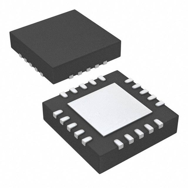
Available in a 4 mm × 4 mm × 0.9 mm QFN
package (RGP)
2 Applications
•
•
•
•
•
Mobile Phones
Tablets
Portable Computers
Keyboards and Mice
Touch Enabled Devices
The boost voltage is set using two external resistors,
and the boost current limit is programmable via the
REXT resistor. The boost converter architecture will not
allow the demand on the supply current to exceed the
limit set by the REXT resistor; therefore, the DRV8662
is well-suited for portable applications. This feature
also allows the user to optimize the DRV8662 circuit
for a given inductor based on the desired performance
requirements.
A typical start-up time of 1.5 ms makes the DRV8662
an ideal piezo driver for fast haptic responses.
Thermal overload protection prevents the device from
being damaged when over driven.
(1)
Device Information
PART NUMBER
DRV8662
(1)
PACKAGE
BODY SIZE (NOM)
VQFN (20)
4.00 mm × 4.00 mm
For all available packages, see the orderable addendum at
the end of the datasheet.
VBAT
L1
CBOOST
Boost
Converter
CPUMP
R1
REXT
DRV8662
R2
IN+
Gain
IN-
+
–
Piezo
Actuator
EN
GAIN0
GAIN1
Simplified Schematic
An IMPORTANT NOTICE at the end of this data sheet addresses availability, warranty, changes, use in safety-critical applications,
intellectual property matters and other important disclaimers. PRODUCTION DATA.
�DRV8662
www.ti.com
SLOS709C – JUNE 2011 – REVISED DECEMBER 2022
Table of Contents
1 Features............................................................................1
2 Applications..................................................................... 1
3 Description.......................................................................1
4 Revision History.............................................................. 2
5 Pin Configuration and Functions...................................3
6 Specifications.................................................................. 4
6.1 Absolute Maximum Ratings........................................ 4
6.2 ESD Ratings............................................................... 4
6.3 Recommended Operating Conditions.........................4
6.4 Thermal Information....................................................5
6.5 Electrical Characteristics.............................................5
6.6 Timing Requirements.................................................. 5
6.7 Typical Characteristics................................................ 6
7 Detailed Description........................................................8
7.1 Overview..................................................................... 8
7.2 Functional Block Diagram........................................... 8
7.3 Feature Description.....................................................9
7.4 Device Functional Modes..........................................10
7.5 Programming.............................................................11
8 Application and Implementation.................................. 12
8.1 Application Information............................................. 12
8.2 Typical Application.................................................... 12
9 Power Supply Recommendations................................17
10 Layout...........................................................................18
10.1 Layout Guidelines................................................... 18
10.2 Layout Example...................................................... 18
11 Device and Documentation Support..........................19
11.1 Documentation Support.......................................... 19
11.2 Trademarks............................................................. 19
12 Mechanical, Packaging, and Orderable
Information.................................................................... 19
4 Revision History
NOTE: Page numbers for previous revisions may differ from page numbers in the current version.
Changes from Revision B (July 2014) to Revision C (December 2022)
Page
• Changed VDD MIN spec from 3.0 to 3.3..............................................................................................................4
Changes from Revision A (November 2012) to Revision B (July 2014)
Page
• Added Device Information and ESD Rating tables, Feature Description section, Device Functional Modes,
Application and Implementation section, Power Supply Recommendations section, Layout section, Device
and Documentation Support section, and Mechanical, Packaging, and Orderable Information section. .......... 1
• Added the Thermal Information table after the Recommend Operating Conditions table. ................................ 5
Changes from Revision * (June 2011) to Revision A (November 2012)
Page
• Added CL, VIL, VIH specs to Recommended Operating Conditions table........................................................... 4
• Added amplifier bandwidth spec (BW) to the Electrical Characteristics table for each gain setting................... 5
2
Submit Document Feedback
Copyright © 2022 Texas Instruments Incorporated
Product Folder Links: DRV8662
�DRV8662
www.ti.com
SLOS709C – JUNE 2011 – REVISED DECEMBER 2022
EN
GAIN1
GAIN0
IN+
IN–
5 Pin Configuration and Functions
20
19
18
17
16
VPUMP
1
15
REXT
VDD
2
14
OUT–
FB
3
13
OUT+
GND
4
12
PVDD
GND
5
11
VBST
6
7
8
9
10
GND
SW
SW
NC
VBST
Figure 5-1. QFN (RGP) Top View
Table 5-1. Pin Functions
PIN
NO. (RGP)
INPUT/ OUTPUT/
POWER (I/O/P)
20
I
Chip enable
FB
3
I
Boost feedback
GAIN0
18
I
Gain programming pin – LSB
NAME
EN
GAIN1
DESCRIPTION
19
I
Gain programming pin – MSB
4, 5, 6
P
Ground
IN+
17
I
Non-inverting input (If unused, connect to GND through capacitor)
IN–
16
I
Inverting input (If unused, connect to GND through capacitor)
OUT+
13
O
Non-inverting output
OUT–
14
O
Inverting output
PVDD
12
P
Amplifier supply voltage
REXT
15
I
Resistor to ground, sets boost current limit
GND
SW
7, 8
P
Internal boost switch pin
VBST
10, 11
P
Boost output voltage
VDD
2
P
Power supply (connect to battery)
VPUMP
1
P
Internal Charge-pump voltage
Submit Document Feedback
Copyright © 2022 Texas Instruments Incorporated
Product Folder Links: DRV8662
3
�DRV8662
www.ti.com
SLOS709C – JUNE 2011 – REVISED DECEMBER 2022
6 Specifications
6.1 Absolute Maximum Ratings
over operating free-air temperature range (unless otherwise noted) (1)
VI
MIN
MAX
UNIT
Supply voltage
VDD
–0.3
6.0
V
Input voltage
IN+, IN–, EN, GAIN0, GAIN1, FB
–0.3
VDD +0.3
V
Boost/Output Voltage
PVDD, SW, OUT+, OUT–
120
V
TA Operating free-air temperature range
–40
70
°C
TJ
–40
150
°C
–65
85
°C
Operating junction temperature range
Storage temperature, Tstg
(1)
Stresses beyond those listed under Absolute Maximum Ratings may cause permanent damage to the device. These are stress
ratings only, which do not imply functional operation of the device at these or any other conditions beyond those indicated under
Recommended Operating Conditions. Exposure to absolute-maximum-rated conditions for extended periods may affect device
reliability.
6.2 ESD Ratings
VALUE
Human-body model (HBM), per ANSI/ESDA/JEDEC
V(ESD)
(1)
(2)
Electrostatic discharge
JS-001(1)
UNIT
±2500
Charged-device model (CDM), per JEDEC specification JESD22C101(2)
V
±1500
JEDEC document JEP155 states that 500-V HBM allows safe manufacturing with a standard ESD control process.
JEDEC document JEP157 states that 250-V CDM allows safe manufacturing with a standard ESD control process.
6.3 Recommended Operating Conditions
over operating free-air temperature range (unless otherwise noted)
MIN
MAX
UNIT
VDD
Supply voltage
VDD
3.3
5.5
V
VBST
Boost voltage
VBST
15
105
V
VIN
CL
1.8(1)
Differential input voltage
Load capacitance
V
VBST = 105 V, Frequency = 500 Hz, VO,PP = 200 V
50
VBST = 105 V, Frequency = 300 Hz, VO,PP = 200 V
100
VBST = 80 V, Frequency = 300 Hz, VO,PP = 150 V
150
VBST = 55 V, Frequency = 300 Hz, VO,PP = 100 V
330
VBST = 30 V, Frequency = 300 Hz, VO,PP = 50 V
680
VBST = 25 V, Frequency = 300 Hz, VO,PP = 40 V
1
VBST = 15 V, Frequency = 300 Hz, VO,PP = 20 V
3
VIL
Digital input low voltage
EN, GAIN0, GAIN1
VDD = 3.6 V
VIH
Digital input high voltage EN, GAIN0, GAIN1
VDD = 3.6 V
REXT
Current limit control resistor
L
Inductance for Boost Converter
(1)
4
TYP
3.3
µF
0.75
V
35
kΩ
1.4
6
nF
V
µH
Gains are optimized for a 1.8V peak input
Submit Document Feedback
Copyright © 2022 Texas Instruments Incorporated
Product Folder Links: DRV8662
�DRV8662
www.ti.com
SLOS709C – JUNE 2011 – REVISED DECEMBER 2022
6.4 Thermal Information
DRV8662
THERMAL METRIC(1)
RGP (20 Pins)
RθJA
Junction-to-ambient thermal resistance
33.1
RθJC(top)
Junction-to-case (top) thermal resistance
30.9
RθJB
Junction-to-board thermal resistance
8.7
ψJT
Junction-to-top characterization parameter
0.4
ψJB
Junction-to-board characterization parameter
8.7
RθJC(bot)
Junction-to-case (bottom) thermal resistance
2.5
(1)
UNIT
°C/W
For more information about traditional and new thermal metrics, see the IC Package Thermal Metrics application report, SPRA953.
6.5 Electrical Characteristics
TA = 25°C, VO,PP = VOUT+ – VOUT– = 200 V, CL = 47 nF, AV = 40 dB, L = 4.7 µH (unless otherwise noted)
PARAMETER
TEST CONDITIONS
MIN
TYP
MAX
UNIT
|IIL|
Digital input low current
EN, GAIN0, GAIN1
VDD = 3.6 V, VIN = 0 V
|IIH|
Digital input high current
EN, GAIN0, GAIN1
VDD = 3.6 V, VIN = VDD
ISD
Shut down current
VDD = 3.6 V, VEN = 0 V
13
µA
VDD = 3.6 V, VEN = VDD, VBST = 105 V, no signal
24
mA
VDD = 3.6 V, VEN = VDD, VBST = 80 V, no signal
13
mA
VDD = 3.6 V, VEN = VDD, VBST = 55 V, no signal
9
mA
VDD = 3.6 V, VEN = VDD, VBST = 30 V, no signal
5
mA
All gains
100
kΩ
GAIN = 00
28.8
GAIN = 01
34.8
GAIN = 10
38.4
GAIN = 11
40.7
IDDQ
Quiescent current
RIN
Input impedance
AV
Amplifier gain
GAIN = 00, VO,PP = 50 V, No Load
BW
Amplifier Bandwidth
10
GAIN = 10, VO,PP = 150 V, No Load
7.5
GAIN = 11, VO,PP = 200 V, No Load
115
VDD = 3.6 V, CL = 47 nF, f = 150 Hz, VO,PP = 200 V
210
VDD = 3.6 V, CL = 47 nF, f = 300 Hz, VO,PP = 200 V
400
Total harmonic distortion plus noise f = 300 Hz, VO,PP = 200 V
µA
dB
kHz
75
VDD = 3.6 V, CL = 10 nF, f = 300 Hz, VO,PP = 200 V
THD+N
5
5
VDD = 3.6 V, CL = 10 nF, f = 150 Hz, VO,PP = 200 V
Average battery current during
operation
µA
20
GAIN = 01, VO,PP = 100 V, No Load
IBAT, AVG
1
mA
1%
6.6 Timing Requirements
MIN
tSU
Start-up time
VDD = 3.6 V, time from EN high until boost and amplifier are fully enabled
TYP
1.5
MAX
UNIT
ms
Submit Document Feedback
Copyright © 2022 Texas Instruments Incorporated
Product Folder Links: DRV8662
5
�DRV8662
www.ti.com
SLOS709C – JUNE 2011 – REVISED DECEMBER 2022
6.7 Typical Characteristics
VDD = 3.6 V, REXT = 7.5 kΩ, L = 4.7 µH, Differential Input
600m
600m
Frequency = 200 Hz
CLOAD = 47 nF
PVDD = 105 V
Gain = 40 dB
VDD = 3.0 V
VDD = 3.6 V
VDD = 5.0 V
400m
VDD = 3.6 V
CLOAD = 47 nF
PVDD = 105 V
Gain = 40 dB
500m
IDD − Supply Current − A
IDD − Supply Current − A
500m
300m
200m
100m
Frequency = 150 Hz
Frequency = 200 Hz
Frequency = 300 Hz
400m
300m
200m
100m
0
0
1
10
100
200
1
10
VOUT − Output Voltage − VPP
Figure 6-1. Supply Current vs Output Voltage
600m
Frequency = 200 Hz
CLOAD = 330 nF
PVDD = 55 V
Gain = 34 dB
VDD = 3.0 V
VDD = 3.6 V
VDD = 5.0 V
400m
VDD = 3.6 V
CLOAD = 330 nF
PVDD = 55 V
Gain = 34 dB
500m
IDD − Supply Current − A
IDD − Supply Current − A
500m
300m
200m
100m
Frequency = 150 Hz
Frequency = 200 Hz
Frequency = 300 Hz
400m
300m
200m
100m
0
0
1
10
100
1
10
VOUT − Output Voltage − VPP
100
VOUT − Output Voltage − VPP
Figure 6-3. Supply Current vs Output Voltage
Figure 6-4. Supply Current vs Output Voltage
600m
600m
Frequency = 200 Hz
CLOAD = 680 nF
PVDD = 30 V
Gain = 28 dB
VDD = 3.0 V
VDD = 3.6 V
VDD = 5.0 V
400m
VDD = 3.6 V
CLOAD = 680 nF
PVDD = 30 V
Gain = 28 dB
500m
IDD − Supply Current − A
500m
IDD − Supply Current − A
200
Figure 6-2. Supply Current vs Output Voltage
600m
300m
200m
100m
Frequency = 150 Hz
Frequency = 200 Hz
Frequency = 300 Hz
400m
300m
200m
100m
0
0
1
10
50
1
VOUT − Output Voltage − VPP
10
50
VOUT − Output Voltage − VPP
Figure 6-5. Supply Current vs Output Voltage
6
100
VOUT − Output Voltage − VPP
Figure 6-6. Supply Current vs Output Voltage
Submit Document Feedback
Copyright © 2022 Texas Instruments Incorporated
Product Folder Links: DRV8662
�DRV8662
SLOS709C – JUNE 2011 – REVISED DECEMBER 2022
10
160
Frequency = 200 Hz
CLOAD = 47 nF
PVDD = 105 V
Gain = 40 dB
VDD = 3.0 V
VDD = 3.6 V
VDD = 5.0 V
VDD = 3.6 V
CLOAD = 47 nF
VOUT = 200 VPP
140
120
OUT+
OUT−
VBST
100
Voltage − V
THD+N − Total Harmonic Distortion + Noise − %
www.ti.com
1
80
60
40
20
0
−20
0.1
20
100
−40
−10m
200
−5m
0
5m
VOUT − Output Voltage − VPP
25m
30m
35m
150
10
Frequency = 200 Hz
CLOAD = 330 nF
PVDD = 55 V
Gain = 34 dB
VDD = 3.0 V
VDD = 3.6 V
VDD = 5.0 V
VDD = 3.6 V
CLOAD = 47 nF
VOUT = 200 VPP
100
OUT+ − OUT−
50
Voltage − V
THD+N − Total Harmonic Distortion + Noise − %
20m
Figure 6-8. Typical Waveform
Figure 6-7. Total Harmonic Distortion + Noise vs
Output Voltage
1
0
−50
−100
0.1
20
−150
−10m
100
−5m
0
5m
VOUT − Output Voltage − VPP
Figure 6-9. Total Harmonic Distortion + Noise vs
Output Voltage
10m 15m
t − Time − s
20m
25m
30m
35m
Figure 6-10. Typical Waveform - Differential
2.5
10
Frequency = 200 Hz
CLOAD = 680 nF
PVDD = 30 V
Gain = 28 dB
VDD = 3.0 V
VDD = 3.6 V
VDD = 5.0 V
2.0
ILIM − Inductor Current − A
THD+N − Total Harmonic Distortion + Noise − %
10m 15m
t − Time − s
1
1.5
1.0
0.5
0.0
0.1
5
10
50
5
10
15
20
25
30
35
REXT − kΩ
VOUT − Output Voltage − VPP
Figure 6-11. Total Harmonic Distortion + Noise vs
Output Voltage
Figure 6-12. ILIM vs REXT
Submit Document Feedback
Copyright © 2022 Texas Instruments Incorporated
Product Folder Links: DRV8662
7
�DRV8662
www.ti.com
SLOS709C – JUNE 2011 – REVISED DECEMBER 2022
7 Detailed Description
7.1 Overview
The DRV8662 accepts the typical battery range used in portable applications (3.0 V to 5.5 V) and creates
a boosted supply rail with an integrated DC-DC converter. This boosted supply rail is fed to an internal,
high-voltage, fully-differential amplifier that is capable of driving capacitive loads such as piezos with signals
up to 200 VPP. No transformer is required for boost operation. Only a single inductor is needed. The boost power
FET and power diode are both integrated within the device.
7.2 Functional Block Diagram
CVDD
L1
VDD
SW
VBST
VPUMP
Charge
Pump
CBOOST
CPUMP
REXT
FB
R1
PVDD
R2
Boost
Control
REXT
EN
DRV8662
OUT-
IN+
Gain
IN-
+
¦
Piezo
Actuator
OUT+
Thermal
Shutdown
GAIN0
8
GAIN1
GND
Submit Document Feedback
Copyright © 2022 Texas Instruments Incorporated
Product Folder Links: DRV8662
�DRV8662
www.ti.com
SLOS709C – JUNE 2011 – REVISED DECEMBER 2022
7.3 Feature Description
7.3.1 Fast Start-up (Enable Pin)
The DRV8662 features a fast startup time, which is essential for achieving low latency in haptic applications.
When the EN pin transitions from low to high, the boost supply is turned on, the input capacitor is pre-charged,
and the amplifier is enabled in a typical 1.5 ms total startup time. In the system application, the entire system
latency should be kept to less than 30 ms total to be imperceptible to the end user. At 1.5 ms, the DRV8662 will
be a small percentage of the total system latency.
7.3.2 Gain Control
The gain from IN+/IN– to OUT+/OUT– is given by the table below.
GAIN1
GAIN0
Gain (dB)
0
0
28.8
0
1
34.8
1
0
38.4
1
1
40.7
The gains are optimized to achieve approximately 50 VPP, 100 VPP, 150 VPP, or 200 VPP at the output without
clipping from a 1.8 V peak single-ended input signal source.
7.3.3 Adjustable Boost Voltage
The output voltage of the integrated boost converter may be adjusted by a resistive feedback divider between
the boost output voltage (VBST) and the feedback pin (FB). The boost voltage should be programmed to a value
greater than the maximum peak signal voltage that the user expects to create with the DRV8662 amplifier. Lower
boost voltages will achieve better system efficiency when lower amplitude signals are applied, so the user should
take care not to use a higher boost voltage than necessary. The maximum allowed boost voltage is 105V.
7.3.4 Adjustable Boost Current Limit
The current limit of the boost switch may be adjusted via a resistor to ground placed on the REXT pin. The
programmed current limit should be less than the rated saturation limit of the inductor selected by the user to
avoid damage to both the inductor and the DRV8662. If the combination of the programmed limit and inductor
saturation is not high enough, then the output current of the boost converter will not be high enough to regulate
the boost output voltage under heavy load conditions. This will, in turn, cause the boosted rail to sag, possibly
causing distortion of the output waveform.
7.3.5 Internal Charge Pump
The DRV8662 has an integrated charge pump to provide adequate gate drive for internal nodes. The output of
this charge pump is placed on the VPUMP pin. An X5R or X7R storage capacitor of 0.1 µF with a voltage rating
of 10 V or greater must be placed at this pin.
7.3.6 Thermal Shutdown
The DRV8662 contains an internal temperature sensor that will shut down both the boost converter and the
amplifier when the temperature threshold is exceeded. When the die temperature falls below the threshold, the
device will restart operation automatically as long as the EN pin is high. Continuous operation of the DRV8662
is not recommended. Most haptic use models only operate the DRV8662 in short bursts. The thermal shutdown
function will protect the DRV8662 from damage when overdriven, but usage models which drive the DRV8662
into thermal shutdown should always be avoided.
Submit Document Feedback
Copyright © 2022 Texas Instruments Incorporated
Product Folder Links: DRV8662
9
�DRV8662
www.ti.com
SLOS709C – JUNE 2011 – REVISED DECEMBER 2022
7.4 Device Functional Modes
7.4.1 Startup/shutdown Sequencing
A simple startup sequence should be employed to maintain smooth haptic operation. If the sequence is not
followed, unintended haptic events or sounds my occur. Use the following steps to play back each haptic
waveform.
7.4.1.1 PWM Source
1. Send 50% duty cycle from the processor to the DRV8662 input filter. This is to allow the source and input
filter to settle before the DRV8662 is fully enabled. At the same time (or on the next available processor
cycle), transition the DRV8662 enable pin from logic low to logic high.
2. Wait 2 ms to ensure that the DRV8662 circuitry is fully enabled and settled.
3. Begin and complete playback of the haptic waveform. The haptic waveform PWM should end with a 50%
duty cycle to bring the differential output back to 0 V.
4. Transition the DRV8662 enable pin from high to low and power down the PWM source.
7.4.1.2 DAC Source
1. Set the DAC to its mid-scale code. This is to allow the source and input capacitors to settle before the
DRV8662 is fully enabled. At the same time (or on the next available processor cycle), transition the
DRV8662 enable pin from logic low to logic high.
2. Wait 2 ms to ensure that the DRV8662 circuitry is fully enabled and settled.
3. Begin and complete playback of the haptic waveform. The haptic waveform should end with a mid-scale
DAC code to bring the differential output back to 0 V.
4. Transition the DRV8662 enable pin from high to low and power down the DAC source.
7.4.2 Low-voltage Operation
The lowest gain setting is optimized for 50 VPP with a boost voltage of 30 V. Some applications may not need
50 VPP, so the user may elect to program the boost converter as low as 15 V to improve efficiency. When using
boost voltages lower than 30 V, some special considerations are in order. First, to reduce boost ripple to an
acceptable level, a 50 V rated, 0.22 µF boost capacitor is recommended. Second, the full-scale input range may
need adjustment to avoid clipping. Normally, a 1.8 V, single-ended PWM signal will give 50 VPP at the lowest
gain. For example, if the boost voltage is set to 25 V for a 40 VPP full-scale output signal, the full-scale input
range drops to 1.44 V for single-ended PWM inputs. An input voltage divider may be desired in this case if a
1.8V I/O is used as a PWM source.
10
Submit Document Feedback
Copyright © 2022 Texas Instruments Incorporated
Product Folder Links: DRV8662
�DRV8662
www.ti.com
SLOS709C – JUNE 2011 – REVISED DECEMBER 2022
7.5 Programming
7.5.1 Programming the Boost Voltage
The boost output voltage (VBST) is programmed via two external resistors as shown in Figure 7-1.
VBST
DRV8662
R1
FB
R2
Figure 7-1. Boost Voltage Programming
The boost output voltage is given by Equation 1:
VBOOST = VFB 1 +
R1
R2
(1)
where VFB = 1.32 V.
VBST should be programmed to a value 5.0 V greater than the largest peak voltage expected in the system
to allow adequate amplifier headroom. Since the programming range for the boost voltage extends to 105 V,
the leakage current through the resistor divider can become significant. It is recommended that the sum of the
resistance of R1 and R2 be greater than 500 kΩ. Note that when resistor values greater than 1 MΩ are used,
PCB contamination may cause boost voltage inaccuracy. Exercise caution when soldering large resistances, and
clean the area when finished for best results.
7.5.2 Programing the Boost Current Limit
The peak current drawn from the supply through the inductor is set solely by the REXT resistor. Note that this
peak current limit is independent of the inductance value chosen, but the inductor should be capable of handling
this programmed limit. The relationship of REXT to ILIM is approximated by Equation 2.
REXT = K
VREF
- RINT
ILIM
(2)
where K = 10500, VREF = 1.35 V, RINT = 60 Ω, and ILIM is the desired peak current limit through the inductor.
Submit Document Feedback
Copyright © 2022 Texas Instruments Incorporated
Product Folder Links: DRV8662
11
�DRV8662
www.ti.com
SLOS709C – JUNE 2011 – REVISED DECEMBER 2022
8 Application and Implementation
Note
Information in the following applications sections is not part of the TI component specification, and
TI does not warrant its accuracy or completeness. TI’s customers are responsible for determining
suitability of components for their purposes. Customers should validate and test their design
implementation to confirm system functionality.
8.1 Application Information
The DRV8662 is typically used in systems that require haptic feedback using high-voltage Piezo actuators.
These systems typically contain an applications processor or microcontroller, which generates a haptic
waveform. This section contains two examples of such systems and how to appropriately configure the input
signal for the DRV8662.
8.2 Typical Application
8.2.1 DRV8662 System Diagram with DAC Input
In the following DRV8662 diagram, the DRV8662 is configured with a differential DAC input and a generic Piezo
actuator. This is useful for systems that have an available DAC or analog signal generator.
L
VBAT
3.0 V - 5.5 V
C2
C1
VDD
SW
VBST PVDD
R1
EN
Digital
Control
FB
GAIN1
R2
GAIN0
VPUMP
C3
DRV8662
REXT
R3
C4
DAC
IN+
OUT+
IN-
OUT-
Piezo
Actuator
C5
GND
Figure 8-1. DRV8662 System Diagram with DAC Input
8.2.1.1 Design Requirements
For this example, use the parameters shown in Table 8-1.
Table 8-1. Design Requirements
12
DESIGN PARAMETER
EXAMPLE VALUE
VDD
3.0V – 5.5V
Boost Converter
20-105V
Output Voltage
2 x Boost Converter (Vpp)
Differential Input Voltage (IN+,
IN-)
1.8Vp Sine wave
Submit Document Feedback
Copyright © 2022 Texas Instruments Incorporated
Product Folder Links: DRV8662
�DRV8662
www.ti.com
SLOS709C – JUNE 2011 – REVISED DECEMBER 2022
Table 8-2 contains a list of components required for configuring the DRV8662. The components labeled
“Standard” can be used “as-is”; and, the components labeled “Configure” require the designer to evaluate
specific system requirements.
Table 8-2. List of Components
COMPONENT
DESCRIPTION
RECOMMENDED VALUE
UNIT
USE
CVDD
VDD bypass capacitor
0.1
µF
Standard
CPUMP
Voltage pump capacitor
0.1
µF
Standard
CIN+ / CIN-
IN+ / IN- AC coupling capacitors
1
µF
Standard
REXT
Boost current limit resistor
See Programing the Boost Current
Limit
Ω
Configure
CPVDD
Boost converter output capacitor
See Boost Capacitor Selection
µF
Configure
L
Boost converter inductor
See Inductor Selection
µH
Configure
R1
Boost converter high-side
feedback resistor
See Programming the Boost
Voltage
Ω
Configure
R2
Boost converter low-side
feedback resistor
SeeProgramming the Boost
Voltage
Ω
Configure
8.2.1.2 Detailed Design Procedure
8.2.1.2.1 Inductor Selection
Inductor selection plays a critical role in the performance of the DRV8662. The range of recommended
inductances is from 3.3 µH to 22 µH. In general, higher inductances within a given manufacturer’s inductor
series have lower saturation current limits, and vice-versa. When a larger inductance is chosen, the DRV8662
boost converter will automatically run at a lower switching frequency and incur less switching losses; however,
larger values of inductance may have higher equivalent series resistance (ESR), which will increase the parasitic
inductor losses. Since lower values of inductance generally have higher saturation currents, they are a better
choice when attempting to maximize the output current of the boost converter. The following table has sample
inductors that provide adequate performance.
For inductor recommendations, see DRV8662EVM User's Guide (SLOU319)
8.2.1.2.2 Piezo Actuator Selection
There are several key specifications to consider when choosing a piezo actuator for haptics such as dimensions,
blocking force, and displacement. However, the key electrical specifications from the driver perspective are
voltage rating and capacitance. At the maximum frequency of 500 Hz, the DRV8662 is optimized to drive
up to 50 nF at 200 VPP, which is the highest voltage swing capability. It will drive larger capacitances if the
programmed boost voltage is lowered and/or the user limits the input frequency range to lower frequencies (e.g.
300 Hz).
For piezo actuator recommendations, see the DRV8662EVM User's Guide (SLOU319).
8.2.1.2.3 Boost Capacitor Selection
The boost output voltage may be programmed as high as 105V. A capacitor with a voltage rating of at least
the boost output voltage must be selected. Since ceramic capacitors tend to come in ratings of 100 V or 250 V,
a 250 V rated 100 nF capacitor of the X5R or X7R type is recommended for the 105 V case. The selected
capacitor should have a minimum working capacitance of at least 50 nF.
8.2.1.2.4 Current Consumption Calculation
It is useful to understand how the voltage driven onto a piezo actuator relates to the current consumption from
the power supply. Modeling a piezo element as a pure capacitor is reasonably accurate. The equation for the
current through a capacitor for an applied sinusoid is given by Equation 3:
ICapacitor (Peak ) = 2p ´ f ´ C ´ VP
(3)
Submit Document Feedback
Copyright © 2022 Texas Instruments Incorporated
Product Folder Links: DRV8662
13
�DRV8662
www.ti.com
SLOS709C – JUNE 2011 – REVISED DECEMBER 2022
where f is the frequency of the sinusoid in Hz, C is the capacitance of the piezo load in farads, and VP is the
peak voltage. At the power supply (usually a battery), the actuator current is multiplied by the boost-supply ratio
and divided by the efficiency of the boost converter as shown by Equation 4.
IBAT (Peak ) = 2p ´ f ´ C ´ VP ´
VBoost
VBAT ´ mBoost
(4)
Substituting typical values for the variables of this equation yields a typical peak current seen by the battery with
a sine input as in Equation 5.
IBAT (Peak ) = 2p ´ 300 Hz ´ 50 nF ´ 100 ´
105
= 392 mA
3.6 ´ 0.7
(5)
8.2.1.2.5 Input Filter Considerations
Depending on the quality of the source signal provided to the DRV8662, an input filter may be required. Some
key factors to consider are whether the source is generated from a DAC or from PWM and the out-of-band
content generated. If proper anti-image rejection filtering is used to eliminate image components, the filter can
possibly be eliminated depending on the magnitude of the out-of-band components. If PWM is used, at least a
1st order RC filter is required. The PWM sample rate should be greater than 30 kHz to keep the PWM ripple from
reaching the piezo element and dissipating unnecessary power. A 2nd order RC filter may be desirable to further
eliminate out-of-band signal content to further drive down power dissipation and eliminate audible noise.
8.2.1.3 Application Curves
150
160
140
120
VDD = 3.6 V
CLOAD = 47 nF
VOUT = 200 VPP
OUT+
OUT−
VBST
100
OUT+ − OUT−
50
Voltage − V
Voltage − V
100
VDD = 3.6 V
CLOAD = 47 nF
VOUT = 200 VPP
80
60
40
0
−50
20
0
−100
−20
−40
−10m
−5m
0
5m
10m 15m
t − Time − s
20m
25m
30m
Figure 8-2. Typical Waveform
14
35m
−150
−10m
−5m
0
5m
10m 15m
t − Time − s
20m
25m
30m
35m
Figure 8-3. Typical Waveform – Differential
Submit Document Feedback
Copyright © 2022 Texas Instruments Incorporated
Product Folder Links: DRV8662
�DRV8662
www.ti.com
SLOS709C – JUNE 2011 – REVISED DECEMBER 2022
8.2.2 DRV8662 System Diagram with Filtered Single-Ended PWM Input
The DRV8662 can be used with a PWM input signal for systems that do not have an available DAC or analog
output. Most piezo actuator systems require a PWM input filter to remove any unwanted noise.
L
VBAT
3.0 V - 5.5 V
C2
C1
VDD
SW
VBST PVDD
R1
EN
Digital
Control
FB
GAIN1
R2
GAIN0
VPUMP
C3
DRV8662
REXT
R3
C4
R4
Processor
IN+
OUT+
IN-
OUT-
Piezo
Actuator
C5
C6
GND
Figure 8-4. DRV8662 System Diagram with Filtered Single-Ended PWM Input
8.2.2.1 Design Requirements
For this example, use the parameters shown in Table 8-3.
Table 8-3. Design Requirements
DESIGN PARAMETER
EXAMPLE VALUE
VDD
3.0V – 5.5V
Boost Converter
20-105V
Output Voltage
2 x Boost Converter (Vpp)
Differential Input Voltage (IN+,
IN-)
1.8Vp PWM
Table 8-4 contains a list of components required for configuring the DRV8662. The components labeled
“Standard” can be used “as-is”; and, the components labeled “Configure” require the designer to evaluate
specific system requirements.
Table 8-4. List of Components
COMPONENT
DESCRIPTION
RECOMMENDED VALUE
UNIT
USE
CVDD
VDD bypass capacitor
0.1
µF
Standard
CPUMP
Voltage pump capacitor
0.1
µF
Standard
CIN+ / CIN-
IN+ / IN- AC coupling
capacitors
1
µF
Standard
Ω
Configure
REXT
Boost current limit resistor See Programing the Boost Current Limit
CPVDD
Boost converter output
capacitor
See Boost Capacitor Selection
µF
Configure
L
Boost converter inductor
See Inductor Selection
µH
Configure
R1
Boost converter high-side
feedback resistor
See Programming the Boost Voltage
Ω
Configure
Submit Document Feedback
Copyright © 2022 Texas Instruments Incorporated
Product Folder Links: DRV8662
15
�DRV8662
www.ti.com
SLOS709C – JUNE 2011 – REVISED DECEMBER 2022
Table 8-4. List of Components (continued)
COMPONENT
R2
DESCRIPTION
Boost converter low-side
feedback resistor
RECOMMENDED VALUE
SeeProgramming the Boost Voltage
UNIT
USE
Ω
Configure
8.2.2.2 Detailed Design Procedure
Use the following section for designing the DRV8662 input filter. See the DRV8662 System with DAC Input
Detailed Design Procedure for the remaining design.
8.2.2.2.1 Input Filter Design
When using a PWM input, a low-pass filter is required. The primary parameters for determining the input filter
are the PWM input frequency and sample rate. Because haptic waveforms are typically less than 500Hz, the
input filter must attenuate frequencies above 500 Hz. For samples rates above 20 kHz, a simple first-order
RC filter is recommended; however, for sample rates much lower (such as 8 kHz), a first-order filter may not
sufficiently attenuate the high-frequency content. Thus, for lower sampling rates, a second-order RC filter may
be required. The DRV8662EVM User's Guide contains example filter configurations for both first-order and
second-order filters. The DRV8662EVM default configuration uses a second-order, differential filter, but it can be
replaced by a first-order, single-ended or differential filter.
1st Order Filter
2nd Order Filter
fin
fs - fin
fs
fs + fin
Apply these criteria to select an input filter:
1. First-order RC filters, both single-ended and differential, are recommended for 20 kHz and higher data
sample rates. The first-order filters have adequate settling time and the fewest components.
2. Second-order filters are recommended for noiseless operation when using a lower data sample rate where a
sharper cutoff is necessary.
3. The attenuation at the PWM carrier frequency should be at least –40 dB for haptic applications.
8.2.2.3 Application Curves
See DRV8662 System with DAC Input Application Curves.
16
Submit Document Feedback
Copyright © 2022 Texas Instruments Incorporated
Product Folder Links: DRV8662
�DRV8662
www.ti.com
SLOS709C – JUNE 2011 – REVISED DECEMBER 2022
9 Power Supply Recommendations
The recommended voltage supply range for the DRV8662 is 2.3V to 5.5V. For proper operation, place a 0.1µF
low equivalent series resistance (ESR) supply-bypass capacitor of X5R or X7R type near the VDD pin with a
voltage rating of at least 10V.
The internal charge pump requires a 0.1µF capacitor of X5R or X7R type with a voltage rating of 10V or greater
be placed between the VPUMP pin and GND for proper operation and stability. Do not use the charge pump as a
voltage source for any other devices.
Submit Document Feedback
Copyright © 2022 Texas Instruments Incorporated
Product Folder Links: DRV8662
17
�DRV8662
www.ti.com
SLOS709C – JUNE 2011 – REVISED DECEMBER 2022
10 Layout
10.1 Layout Guidelines
•
•
To achieve optimum device performance, use of the thermal footprint outlined by this datasheet is
recommended. See land pattern diagram for exact dimensions. The DRV8662 power pad must be soldered
directly to the thermal pad on the printed circuit board. The printed circuit board thermal pad should be
connected to the ground net with thermal vias to any existing backside/internal copper ground planes.
Connection to a ground plane on the top layer near the corners of the device is also recommended.
Another key layout consideration is to keep the boost programming resistors (R1 and R2) as close as
possible to the FB pin of the DRV8662. Care should be taken to avoid getting the FB trace near the SW
trace.
10.2 Layout Example
Figure 10-1. Layout Example
18
Submit Document Feedback
Copyright © 2022 Texas Instruments Incorporated
Product Folder Links: DRV8662
�DRV8662
www.ti.com
SLOS709C – JUNE 2011 – REVISED DECEMBER 2022
11 Device and Documentation Support
11.1 Documentation Support
11.1.1 Related Documentation
DRV8662EVM User's Guide (SLOU319)
DRV8662 Configuration Guide (SLOA198)
11.2 Trademarks
All trademarks are the property of their respective owners.
12 Mechanical, Packaging, and Orderable Information
The following pages include mechanical, packaging, and orderable information. This information is the most
current data available for the designated devices. This data is subject to change without notice and revision of
this document. For browser-based versions of this data sheet, refer to the left-hand navigation.
Submit Document Feedback
Copyright © 2022 Texas Instruments Incorporated
Product Folder Links: DRV8662
19
�PACKAGE OPTION ADDENDUM
www.ti.com
18-Oct-2022
PACKAGING INFORMATION
Orderable Device
Status
(1)
Package Type Package Pins Package
Drawing
Qty
Eco Plan
(2)
Lead finish/
Ball material
MSL Peak Temp
Op Temp (°C)
Device Marking
(3)
Samples
(4/5)
(6)
DRV8662RGPR
ACTIVE
QFN
RGP
20
3000
RoHS & Green
NIPDAU
Level-4-260C-72 HR
-40 to 70
8662
Samples
DRV8662RGPT
ACTIVE
QFN
RGP
20
250
RoHS & Green
NIPDAU
Level-4-260C-72 HR
-40 to 70
8662
Samples
(1)
The marketing status values are defined as follows:
ACTIVE: Product device recommended for new designs.
LIFEBUY: TI has announced that the device will be discontinued, and a lifetime-buy period is in effect.
NRND: Not recommended for new designs. Device is in production to support existing customers, but TI does not recommend using this part in a new design.
PREVIEW: Device has been announced but is not in production. Samples may or may not be available.
OBSOLETE: TI has discontinued the production of the device.
(2)
RoHS: TI defines "RoHS" to mean semiconductor products that are compliant with the current EU RoHS requirements for all 10 RoHS substances, including the requirement that RoHS substance
do not exceed 0.1% by weight in homogeneous materials. Where designed to be soldered at high temperatures, "RoHS" products are suitable for use in specified lead-free processes. TI may
reference these types of products as "Pb-Free".
RoHS Exempt: TI defines "RoHS Exempt" to mean products that contain lead but are compliant with EU RoHS pursuant to a specific EU RoHS exemption.
Green: TI defines "Green" to mean the content of Chlorine (Cl) and Bromine (Br) based flame retardants meet JS709B low halogen requirements of


 工商网监
湘ICP备2023018690号
工商网监
湘ICP备2023018690号
