Product
Folder
Sample &
Buy
Technical
Documents
Support &
Community
Tools &
Software
DRV8808
SLVS857B – DECEMBER 2009 – REVISED JANUARY 2015
DRV8808 Combination Motor Driver With DC-DC Converter
1 Features
3 Description
•
The DRV8808 device provides the integrated motor
driver solution for printers. The chip has three full Hbridges and three buck DC-DC converters.
1
•
•
•
•
•
•
•
•
Three DC Motor Drivers
– Up to 2.5-A Current Chopping
– Low Typical ON Resistance (RDSON = 0.5 Ω at
TJ = 25°C)
Three Integrated DC-DC Converters
– ON/OFF Selectable Using CSELECT Pin and
Serial Interface
– Outputs Configurable With External Resistor
Network From 1 V to 90% of VM Capability for
All Three Channels
– 1.35-A Output Capability for All Three
Channels
One Integrated LDO Regulator
– Output Configurable With External Resistor
Network from 1 V to 2.5 V
– 550-mA Output Capability
7-V to 40-V Operating Range
Serial Interface for Communications
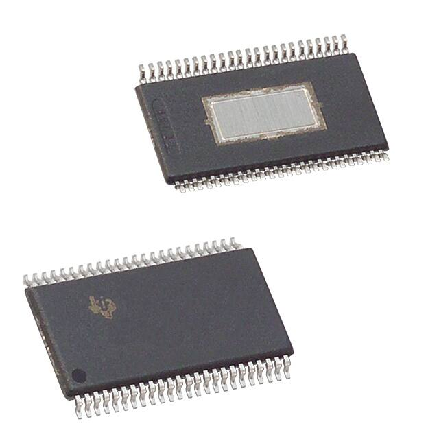
Thermally Enhanced Surface-Mount Package
48-Pin HTSSOP With PowerPAD™
(Eco-Friendly: RoHS and No Sb/Br )
Power-Down Function (Deep-Sleep Mode)
Reset Signal Output (Active Low)
Reset (All Clear) Control Input
2 Applications
•
•
•
•
Printers
Document Scanners
POS
Copiers
The output driver block for each consists of Nchannel power MOSFETs configured as full Hbridges to drive the motor windings. The device can
be configured to use internal or external current
sense for winding current control.
The SPI input pins are 3.3-V compatible and have
inputs that are 5-V tolerant.
The DRV8808 has three DC-DC switched-mode buck
converters to generate a programmable output
voltage from 1 V up to 90% of VM, with up to 1.35-A
load current capability.
The device is configured using the CSELECT
terminal at start-up, and serial interface during run
time.
An internal shutdown function is provided for
overcurrent protection, short-circuit protection,
undervoltage lockout, and thermal shutdown. Also,
the device has the reset function at power on, and
the input on the nReset pin.
Device Information(1)
PART NUMBER
PACKAGE
DRV8808
BODY SIZE (NOM)
HTSSOP (48)
12.50 mm x 6.10 mm
(1) For all available packages, see the orderable addendum at
the end of the datasheet.
Typical Application Schematic
VIN
VM
VM
A+
OD_A
DC/DC
convertor
Ch-A
Motor Drive
Output
Control A
VM
DC
Motor
A-
FBA
RSA
Optional
OD_B
DC/DC
convertor
Ch-B
FBB
B+
Motor Drive
Output
Control B
VM
DC
Motor
BRSB
Optional
OD_C
DC/DC
convertor
Ch-C
C+
Motor Drive
Output
Control C
FBC
LDO_IN
VM
DC
Motor
CRSC
Optional
LDO
Regulator
LDO_OUT
LDO_FB
1
An IMPORTANT NOTICE at the end of this data sheet addresses availability, warranty, changes, use in safety-critical applications,
intellectual property matters and other important disclaimers. PRODUCTION DATA.
�DRV8808
SLVS857B – DECEMBER 2009 – REVISED JANUARY 2015
www.ti.com
Table of Contents
1
2
3
4
5
6
Features ..................................................................
Applications ...........................................................
Description .............................................................
Revision History.....................................................
Pin Configuration and Functions .........................
Specifications.........................................................
6.1
6.2
6.3
6.4
6.5
6.6
7
1
1
1
2
3
6
Absolute Maximum Ratings ..................................... 6
ESD Ratings.............................................................. 6
Recommended Operating Conditions....................... 6
Thermal Information .................................................. 6
Electrical Characteristics........................................... 7
Typical Characteristics ............................................ 11
Detailed Description ............................................ 12
7.1 Overview ................................................................. 12
7.2 Functional Block Diagram ....................................... 13
7.3 Feature Description................................................. 14
7.4 Device Functional Modes........................................ 32
7.5 Programming........................................................... 32
8
Application and Implementation ........................ 36
8.1 Application Information............................................ 36
8.2 Typical Application ................................................. 36
9 Power Supply Recommendations...................... 38
10 Layout................................................................... 38
10.1 Layout Guidelines ................................................. 38
10.2 Layout Example .................................................... 38
11 Device and Documentation Support ................. 39
11.1 Trademarks ........................................................... 39
11.2 Electrostatic Discharge Caution ............................ 39
11.3 Glossary ................................................................ 39
12 Mechanical, Packaging, and Orderable
Information ........................................................... 39
4 Revision History
Changes from Revision A (August 2011) to Revision B
•
2
Page
Added ESD Ratings table, Feature Description section, Device Functional Modes, Application and Implementation
section, Power Supply Recommendations section, Layout section, Device and Documentation Support section, and
Mechanical, Packaging, and Orderable Information section .................................................................................................. 1
Submit Documentation Feedback
Copyright © 2009–2015, Texas Instruments Incorporated
Product Folder Links: DRV8808
�DRV8808
www.ti.com
SLVS857B – DECEMBER 2009 – REVISED JANUARY 2015
5 Pin Configuration and Functions
DCA Package
48-Pins HTSSOP
Top View
OD_A
OD_C
GND
FB_C
CSELECT
TH_OUT
LOGIC_OUT
nORT
ENABLE_A/STROBE
48
47
46
45
44
43
42
41
40
39
38
37
36
35
34
33
32
31
30
29
28
27
26
25
1
2
3
4
5
6
7
8
9
10
11
12
13
14
15
16
17
18
19
20
21
22
23
24
PHASE_A/CLK
ENABLE_B
PHASE_B
ENABLE_C
PHASE_C/DATA
A_CONT
NC
V3P3
nSLEEP
nRESET
nWAKEUP
VLDO_OUT
VLDO_FB
VLDO_IN
FB_B
FB_A
GND
COA
CP2
VCP
VM
C–
RSC/GND
RSC/GND
C+
VM
VM
B–
RSB/GND
RSB/GND
B+
VM
A+
RSA/GND
RSA/GND
A–
VM
GND
OD_B
Pin Functions
PIN
NAME
NO.
I/O
PU/PD
SHUNT
R
DESCRIPTION
A-
28
O
—
—
Motor drive output for winding A-
A+
31
O
—
—
Motor drive output for winding A+
A_CONT
15
I
Down
100k
B-
36
O
—
—
Motor drive output for winding B-
B+
33
O
—
—
Motor drive output for winding B+
C-
42
O
—
—
Motor drive output for winding C-
C+
39
O
—
—
Motor drive output for winding C+
CP1
46
O
—
—
Charge pump bucket capacitor output (low side)
CP2
45
O
—
—
Charge pump bucket capacitor output (high side)
CSELECT
5
I
Up
200k
DC-DC converter startup selector
ENA / STB
9
I
Down
100k
Enable input for DC motor A control / SPI STROBE
ENB
11
I
Down
100k
Enable input for DC motor B control
ENC
13
I
Down
100k
Enable input for DC motor C control
FB_A
48
I
—
—
Feedback signal for DC-DC converter A
FB_B
24
I
—
—
Feedback signal for DC-DC converter B
FB_C
4
I
—
—
Feedback signal for DC-DC converter C
GND
3
—
—
—
Ground
GND
26
—
—
—
Ground
GND
47
—
—
—
Ground
DC-DC A converter control (L = Enable)
Submit Documentation Feedback
Copyright © 2009–2015, Texas Instruments Incorporated
Product Folder Links: DRV8808
3
�DRV8808
SLVS857B – DECEMBER 2009 – REVISED JANUARY 2015
www.ti.com
Pin Functions (continued)
PIN
NAME
NO.
I/O
PU/PD
SHUNT
R
DESCRIPTION
LOGIC_OUT
7
O
—
—
Information monitoring output (open drain)
NC
16
NC
—
—
Do not connect
nORT
8
O
—
—
Reset output (open drain)
nReset
19
I
Up
200k
Reset input (L: reset, H/open: normal operation)
nSLEEP
18
I
Down
100k
Enable/disable, SPI selector
nWAKEUP
20
I
Up
200k
Wake-up pin for DeepSleep mode (L = WAKEUP)
OD_A
1
O
—
—
Output for DC-DC switch mode regulator A
OD_B
25
O
—
—
Output for DC-DC switch mode regulator B
OD_C
2
O
—
—
Output for DC-DC switch mode regulator C
PHA / CLK
10
I
Down
100k
Phase input for DC motor A control / SPI CLOCK
PHB
12
I
Down
100k
Phase input for DC motor B control
PHC / DATA
14
I
Down
100k
Phase input for DC motor C control / SPI DATA
RSA / GND
30
O
—
—
Motor drive current sensing resistor A / GND power
RSKA / GND
29
I
—
—
Motor drive current sensing resistor A / GND Kelvin
RSB / GND
35
O
—
—
Motor drive current sensing resistor B / GND power
RSKB / GND
34
I
—
—
Motor drive current sensing resistor B / GND Kelvin
RSC / GND
41
O
—
—
Motor drive current sensing resistor C / GND power
RSKC / GND
40
I
—
—
Motor drive current sensing resistor C / GND Kelvin
TH_OUT
6
O
—
—
Temperature warning output (open drain)
V3p3
17
O
—
—
Bypass for internal 3.3-V regulator
VCP
44
O
—
—
Charge pump output
VLDO_FB
22
I
—
—
LDO voltage regulator feed back
VLDO_IN
23
I
—
—
LDO voltage regulator input
VLDO_OUT
21
O
—
—
LDO voltage regulator output
VM
27
—
—
—
Voltage supply for motors and regulators
VM
32
—
—
—
Voltage supply for motors and regulators
VM
37
—
—
—
Voltage supply for motors and regulators
VM
38
—
—
—
Voltage supply for motors and regulators
VM
43
—
—
—
Voltage supply for motors and regulators
4
Submit Documentation Feedback
Copyright © 2009–2015, Texas Instruments Incorporated
Product Folder Links: DRV8808
�DRV8808
www.ti.com
SLVS857B – DECEMBER 2009 – REVISED JANUARY 2015
Internal
3.3-V
Supply
200 kW
(±40%)
1) Pin open, 3 V to 3.3 V
A /OFF, B /ON, C /ON
2) External R to GND (200 kW ± 10%)
1.3 V to 2 V
A /OFF, B /ON, C /OFF
3) GND, 0 V to 0.3 V
A /OFF, B /OFF, C /OFF
# CSELECT
Soft-Start
Control
GND
# Enable_X
# Phase _X
Hysteresis
# nSLEEP
# A_CONT
Serial Interface
100 kW
(±30%)
GND GND
Internal
3.3-V
Supply
200 kW
(±40%)
# nWAKEUP
Hysteresis
Deglitch
# nReset
GND
Reset Control
Deglitch is for nReset only.
nReset pulled up to 3.3 V internal.
nWAKEUP pulled up to 8 V internal.
Figure 1. Input Pin Configuration
External
3.3-V
Supply
# TH_OUT
1 kW
(External)
# LOGIC_OUT
# nORT
GND
Figure 2. Open-Drain Output Pin Configuration
Submit Documentation Feedback
Copyright © 2009–2015, Texas Instruments Incorporated
Product Folder Links: DRV8808
5
�DRV8808
SLVS857B – DECEMBER 2009 – REVISED JANUARY 2015
www.ti.com
6 Specifications
6.1 Absolute Maximum Ratings (1)
over operating free-air temperature range (unless otherwise noted)
MIN
VM
MAX
UNIT
40
V
Supply voltage
Logic input voltage, serial I/F, A_CONT, nReset, and so forth
(2)
–0.3
5.5
V
TH_OUT, nORT, LOGIC_OUT, CSELECT
–0.3
3.6
V
nWAKEUP
–0.3
8
V
Continuous total power dissipation (in case θJA = 20°C/W)
TJ
4
W
Continuous motor-drive output current for each H-bridge (100 ms)
2.5
A
Continuous DC-DC converter output current (3)
1.35
A
Operating junction temperature (1 hour)
190
°C
Lead temperature 1.6 mm (1/16 in) from case for 10 s
260
°C
150
°C
Tstg Storage temperature
(1)
(2)
(3)
–65
Stresses beyond those listed under Absolute Maximum Ratings may cause permanent damage to the device. These are stress ratings
only and functional operation of the device at these or any other conditions beyond those indicated under Recommended Operating
Conditions is not implied. Exposure to absolute-maximum-rated conditions for extended periods may affect device reliability.
The negative spike less than –5 V and narrower than 50-ns width should not cause any problem.
May shut down due to regulator OCP.
6.2 ESD Ratings
VALUE
Human-body model (HBM), per ANSI/ESDA/JEDEC JS-001
V(ESD)
(1)
(2)
Electrostatic discharge
(1)
UNIT
±2000
Charged-device model (CDM), per JEDEC specification JESD22C101 (2)
V
±500
JEDEC document JEP155 states that 500-V HBM allows safe manufacturing with a standard ESD control process.
JEDEC document JEP157 states that 250-V CDM allows safe manufacturing with a standard ESD control process.
6.3 Recommended Operating Conditions
MIN NOM
Supply voltage range, VM for motor control
Supply voltage range for DC-DC converter (VM)
MAX
UNIT
18
27
38
V
7
27
38
V
Operating ambient temperature range
–10
85
°C
Operating junction temperature range
0
135
°C
6.4 Thermal Information
DRV8808
THERMAL METRIC (1)
HTSSOP (DCA)
UNIT
48 PINS
RθJA
Junction-to-ambient thermal resistance
28.1
RθJC(top)
Junction-to-case (top) thermal resistance
15.6
RθJB
Junction-to-board thermal resistance
10.2
ψJT
Junction-to-top characterization parameter
0.3
ψJB
Junction-to-board characterization parameter
10.1
RθJC(bot)
Junction-to-case (bottom) thermal resistance
0.9
(1)
6
°C/W
For more information about traditional and new thermal metrics, see the IC Package Thermal Metrics application report, SPRA953.
Submit Documentation Feedback
Copyright © 2009–2015, Texas Instruments Incorporated
Product Folder Links: DRV8808
�DRV8808
www.ti.com
SLVS857B – DECEMBER 2009 – REVISED JANUARY 2015
6.5 Electrical Characteristics
TJ = 0°C to 135°C, VM = 7 V to 38 V (unless otherwise noted)
PARAMETER
TEST CONDITIONS
MIN
TYP
MAX
UNIT
SUPPLY (SLEEP) CURRENT
ISLEEP1
Supply (sleep) current 1
nSLEEP = L,
DC-DC all off
3
5.5
mA
ISLEEP2
Supply (sleep) current 2
nSLEEP = L,
Regulators enabled
VM = 8 V,
No load
6
8
mA
ISLEEP3
Supply (sleep) current 3
nSLEEP = L,
Regulators enabled
VM = 38 V,
No load
6
8
mA
IDEEP_SL
Supply (deep sleep) current (1)
VM = 38 V
0.7
1
mA
DIGITAL INTERFACE CIRCUIT
VIH
Digital high-level input voltage
Digital inputs
3.6
V
IIH
Digital high-level input current
Digital inputs
2
100
μA
VIL
Digital low-level input voltage
Digital inputs
0.8
V
IIL
Digital low-level input current
Digital inputs
100
μA
Vhys
Digital input hysteresis
Digital inputs
Tdeg_nReset
nReset input deglitch time
2.5
7.5
μs
Tfilt_ACONT
A_CONT filter time (2)
30
70
μs
0.45
V
CHARGE-PUMP VCP (CP = 0.1 μF to 0.47 μF, Cblk = 0.01 μF ±20%)
VO(CP)
Output voltage
f(CP)
Switching frequency
tstart
Start-up time
ILOAD = 0 mA,
VM > 15 V
VM + 10
VM + 13
1.6
CStorage = 0.1 μF,
VM ≥ 15 V
V
MHz
0.5
2
ms
V3P3 OUTPUT
V3p3
Output voltage (3)
3
3.3
3.6
V
Cbypass
Output capacitor
0.08
0.1
10
μF
5.76
6.4
7.04
MHz
INTERNAL CLOCK OSCI
fOSCi
System clock rrequency
CSELECT FOR DC-DC STARTUP SELECTION
VCS0
DC-DC all off
VCS1
Turn ON ODB
Pull down by external 200-kΩ resistor
VCS2
Turn ON ODB then ODC
As pin open
VLDO REGULATOR
LDO input voltage
VLDOFB
Feedback voltage
VLDOOUT
Output voltage range
IOUT
Load capability
IOCP
OCP current
tIdeg
OCP deglitch
V
3
3.6
V
3.6
V
1
1 V ≤ VLDOOUT ≤ 1.8 V
±5%
1.8 V ≤ VLDOOUT ≤ 2.5 V
±3%
Vovp
Overvoltage protection
Vuvp
Undervoltage protection
% to nominal Voutx detected at VFB
(VFB decreasing)
(6)
V
2
3
% to nominal Voutx detected at VFB
(VFB increasing)
(2)
(3)
(4)
(5)
0.3
(4) (5) (6)
VLDOIN
(1)
0
1.3
V
500
mA
725
1100
mA
3
8
13
μs
25%
30%
35%
–25%
–30%
–35%
Deep Sleep shuts down majority of the device and runs minimal circuits (internal bias circuits and the nWAKEUP pin). Deep Sleep is
entered by writing 1 to Setup Register, Bank 1, Bit 11. Device is restarted by pulling nWAKEUP pin low or power cycling VM. Deep
Sleep functionality only available for VM > VthVM+.
A_CONT is filtered for both high and low levels.
V3p3 bypass pin is not meant to be used as a supply.
LDO can be bypassed by either load configuration 1 or 2.
Typical values for external components should be chosen such that when the tolerance is added to the typical, the values remain
between the maximum and minimum specifications listed.
When LDO is not used, recommend connecting VLDO_IN to GND, VLDO_OUT to GND, and VLDO_FB to FB_B.
Submit Documentation Feedback
Copyright © 2009–2015, Texas Instruments Incorporated
Product Folder Links: DRV8808
7
�DRV8808
SLVS857B – DECEMBER 2009 – REVISED JANUARY 2015
www.ti.com
Electrical Characteristics (continued)
TJ = 0°C to 135°C, VM = 7 V to 38 V (unless otherwise noted)
PARAMETER
tVdeg
TEST CONDITIONS
UVP/OVP deglitch time
CL1
Electrolytic load capacitance
CESR1
Load bypass configuration 1
ESR of load capacitance
CC1
Ceramic load capacitance
CL2
Electrolytic load capacitance
CESR2
Load bypass configuration 2
CC2
MIN
TYP
3
8
MAX
UNIT
13
μs
27
120
μF
0.05
2
Ω
0.4
μF
120
μF
0
80
100
0.05
0.2
Ω
0
3
μF
Vth VM- < VM < 7 V
0.8 x
VM
V
20 V < VM < 38 V
0.9 x
VM
ESR of load capacitance
Ceramic load capacitance
THREE DC-DC CONVERTER
VM
OPE_X
ODx
Operating supply voltage range
ratio to VOUT
Regulator output voltage
IO < 0.6 A
20 V < VM < 40 V
0℃ < TJ < 125℃
-3%
VO
3%
125℃ < TJ < 135℃
-4%
VO
4%
6.5 V < VM < 20 V
-5%
VO
5%
VM = 7 V, VO = 5.5 V
-5%
VO
5%
0℃ < TJ < 125℃
-3%
VO
3%
125℃ < TJ < 135℃
-4%
VO
4%
-5%
VO
5%
VM = 7 V, VO = 1 V
VthVM- < VM < 6.5 V , VO ≤ 3.3 V
FBx
FBx pin voltage
IO ODx
Output current (DC)
VM > 15 V
1.35
A
IO ODx2
Output current (DC) at low VM
VM = 7 V, VO = 5.5 V
0.6
A
IO ODx3
Output current (DC) at low VM
VM = 7 V, VO = 3.3 V
1.2
A
RDSON (7)
FET on-resistance at 0.8 A for
OD_x VM > 15 V
TJ = 70 °C
0.85
1.05
Ω
1
1.2
L
Inductor
VOUT = 1.0 V
150
VOUT ≥ 3.3 V
330
C
Capacitor
1
TJ = 135 °C
VOUT = 1.0 V
270
VOUT ≥ 3.3 V
V
μH
330
μF
2.7
A
220
THREE DC-DC CONVERTER PROTECTION
IO DD ODx
Overcurrent detect for OD_x
source
tODXdeg
Cycle by cycle Idetect deglitch
tODXSD
DC-DC shutdown filter
Number of consecutive cycles with Idetect
Vovpx
Overvoltage protection
% to nominal Voutx detected at VFB
(VFB increasing)
25%
30%
35%
Vuvpx
Undervoltage protection
% to nominal Voutx detected at VFB
(VFB decreasing)
–25%
–30%
–35%
tVXdeg
UVP/OVP deglitch time
3
8
13
μs
tsst
Start-up time with soft start
56
ms
Vstover
Start-up overshoot
VM SUPERVISORY (8)
Peak current in each ON cycle
1.35
100
200
400
4
Ratio to Vo
ns
chop
cycles
3%
(9)
VthVM–
nORT, for VM low threshold
VM decreasing
4.5
5
6
V
VthVM+
nORT, for VM high threshold
VM increasing
5.5
6
6.79
V
(7)
(8)
(9)
8
RDSON at T = 135°C guaranteed by characterization. Production test will be done at T = 25°C/70°C.
VM must be VM > VthVM+ to start up internal DC-DC converter.
When VM goes down below VthVM+, the VUVPx (undervoltage protection in DC-DC) are masked. The DC-DC converter is shut off by
nORT assertion at VthVM –.
Submit Documentation Feedback
Copyright © 2009–2015, Texas Instruments Incorporated
Product Folder Links: DRV8808
�DRV8808
www.ti.com
SLVS857B – DECEMBER 2009 – REVISED JANUARY 2015
Electrical Characteristics (continued)
TJ = 0°C to 135°C, VM = 7 V to 38 V (unless otherwise noted)
PARAMETER
TEST CONDITIONS
VthVMh
nORT, for VM detect hysteresis
VthVM2
For motor driver off (10)
tVMfilt
Vth VM monitor filtering time
For Vth VM detect
tVM2filt
Vth VM2 monitor filtering time
For Vth VM2 detect
THERMAL SHUTDOWN: TSD
TYP
0.5
1
MAX
UNIT
V
15
V
4
30
μs
30
60
ms
(11) (12)
TTSD
Thermal shutdown set points
tTSDdeg
TSD deglitch time
TEMPERATURE WARNING: PRE-TSD
PreTSD
VthVM+ – VthVM–
MIN
150
170
190
°C
30
60
90
μs
115
135
155
°C
(13) (12)
Temperature warning
Assert at TH_OUT pin
OPEN-DRAIN OUTPUTS (NORT, LOGIC_OUT, TH_OUT)
VOH
High-state voltage
RL = 1 kΩ to 3.3 V
Low-state voltage
RL = 1 kΩ to 3.3 V
IOL (14)
Low-state sink current
Vo = 0.25 V
tr (15)
Rise time
10% to 90%
1
μs
tf (15)
Fall time
90% to 10%
50
ns
(14)
VOL
NORT DELAY: STARTUP SEQUENCE
3
V
0.3
2
V
mA
(16) (17)
Tord1
nORT delay 1
Reset deassertion from VthVM+ < VM, for
DC/DC wake up failing
Tord3
DC-DC turn on delay
From one DC-DC wake up to following DCDC to go soft-start sequence
Tord4
nORT delay 4
Reset deassertion from 2nd DC-DC wake up
200
300
390
ms
5
10
15
ms
60
120
180
ms
5
10
μs
NRESET INPUT (16)
Treset
nReset assertion to nORT
assertion delay
nReset falling to nORT failing
H-BRIDGE DRIVERS (OUTX+ AND OUTX–) CONDITION: VM = 15 V to 38 V
(18)
IOUT1(max)
Peak output current 1
Less than 500-ns period
6.8
A
IOUT2(max)
Peak output current 2
Less than 100-ms period
2.42
A
RDSON
FET ON resistance at 0.8 A
TJ = 70°C
0.55
0.65
Ω
TJ = 135°C
0.7
0.85
ICEX
Output leakage current
IOC Motor
Motor overcurrent threshold for
each H-bridge (18)
Fchop
Motor chopping frequency =
FOSCM/8
VOUTX = 0 V or 10
3
90
100
10
μA
8
A
110
kHz
DC MOTOR DRIVERS
tr
Rise time
VM = 35 V
20% to 80%
50
200
ns
tf
Fall time
VM = 35 V
20% to 80%
50
200
ns
tPDOFF
Enable or strobe detection
to sink or source gate OFF delay
400
ns
(10)
(11)
(12)
(13)
(14)
(15)
(16)
(17)
(18)
50
150
No nORT assertion to VthVM2 detection.
TSD does not need thermal hysteresis.
Parametric guaranteed by characterization. Not tested in production.
PreTSD does not need thermal hysteresis.
Production test only measures Vol and Iol to ensure timing.
tr and tf dominated by external capacitance, pullup resistance, and open-drain NMOS RDSON.
This includes asynchronous timing deviation between the event to the timer clock.
nORT assertion delay is configurable and defined in the serial register section.
When the overcurrent is detected, all the H-bridges are shut down and assert nORT per shutdown configuration.
Submit Documentation Feedback
Copyright © 2009–2015, Texas Instruments Incorporated
Product Folder Links: DRV8808
9
�DRV8808
SLVS857B – DECEMBER 2009 – REVISED JANUARY 2015
www.ti.com
Electrical Characteristics (continued)
TJ = 0°C to 135°C, VM = 7 V to 38 V (unless otherwise noted)
PARAMETER
tCOD
Crossover delay time to prevent
shoot through
tPDON
Enable or strobe detection
to sink or source gate ON delay
tIdeg
MISD BLANK
TEST CONDITIONS
TBLANK
VRSTRIP
Internal current trip
External resistor sense voltage
trip threshold
TYP
MAX
UNIT
(19)
600
1000
ns
100
750
[00] (20)
ns
1.80
2.25
2.95
[01]
(21)
1.20
1.50
2.30
[10]
(22)
2.35
3.00
3.65
[11] (23)
Tblank
MIN
2.95
3.75
4.30
[00]
(24)
3.05
3.45
5.50
[01]
(25)
1.90
2.20
4.15
[10]
(26)
4.15
4.70
6.75
[11] (27)
5.30
5.95
8.25
00
1.18
1.4
1.62
01
1.48
1.7
1.92
10
1.68
1.9
2.12
11
1.98
2.2
2.42
00
165
185
205
01
190
210
230
10
240
260
280
11
290
310
330
Pminp
Minimum pulse width (phase)
(19)
Pmine
Minimum pulse width (enable)
(19)
μs
μs
A
mV
1
μs
1
μs
25
MHz
SERIAL INTERFACE (28)
f(CLK)
Clock frequency
twh(CLK)
Minimum high-level pulse width
10
ns
twl(CLK)
Minimum low-level pulse width
10
ns
tdcs
Setup time, DATA to CLK↓
10
ns
tdch
Hold time, CLK↓ to DATA
10
ns
tdss
Setup time, DATA to STROBE↑
10
ns
tdsh
Hold time, STROBE↑ to DATA
10
ns
tcss
Setup time, CLK↓ to STROBE↑
20
(29)
ns
tcsh
Hold time, STROBE↑ to CLK↓
20 (29)
ns
tnss
Setup time, nSLEEP↓ to
STROBE↑
4 (30)
μs
tnsh
Hold time, STROBE↑ to
nSLEEP↑
10
ns
tw(STRB)
Minimum strobe pulse width
20
ns
(19)
(20)
(21)
(22)
(23)
(24)
(25)
(26)
(27)
(28)
(29)
tCOD, Pminp, and Pmine not production tested.
3 to 4 periods Fosc/4 + 1 Fosc
2 to 3 periods Fosc/4 + 1 Fosc
4 to 5 periods Fosc/4 + 1 Fosc
5 to 6 periods Fosc/4 + 1 Fosc
3 Fosc/8 (can add up to 1 additional Fosc/8 + 1.5 Fosc at phase or enable change due to asynchronous ambiguity)
2 Fosc/8 (can add up to 1 additional Fosc/8 + 1.5 Fosc at phase or enable change due to asynchronous ambiguity)
4 Fosc/8 (can add up to 1 additional Fosc/8 + 1.5 Fosc at phase or enable change due to asynchronous ambiguity)
5 Fosc/8 (can add up to 1 additional Fosc/8 + 1.5 Fosc at phase or enable change due to asynchronous ambiguity)
Serial interface timing will not be tested parametrically in production.
DATA value at STROBE is address bit for Setup and Extended Setup register so setup and hold times apply to DATA relative to
STROBE. CLK and DATA also require setup and hold times relative to each other. Therefore, CLK and STROBE setup and hold timing
is the summation of both.
(30) Internal filter on nSLEEP to STROBE drives this specification.
10
Submit Documentation Feedback
Copyright © 2009–2015, Texas Instruments Incorporated
Product Folder Links: DRV8808
�DRV8808
www.ti.com
SLVS857B – DECEMBER 2009 – REVISED JANUARY 2015
Electrical Characteristics (continued)
TJ = 0°C to 135°C, VM = 7 V to 38 V (unless otherwise noted)
PARAMETER
TEST CONDITIONS
MIN
SERIAL INTERFACE: ID MONITOR FUNCTION AT LOGIC_OUT PIN, EXTENDED SETUP MODE
tODL
0 data output delay bit 3 to 0
(ext-setup) = (1100)
tODH
1 data output delay bit 3 to 0
(ext-setup) = (1111)
TYP
MAX
UNIT
4000
ns
4000
ns
(31)
From strobe rise to Logic_out
(1 kΩ to external 3.3 V)
(31) Serial interface timing will not be tested parametrically in production.
6.6 Typical Characteristics
3.00%
2.00%
2.00
Output Accuracy (%)
Tsense Output Voltage (V)
2.20
1.80
1.60
30
60
90
120
Temperature (C)
150
-1.00%
1.8V
3.3V
Linear
0
0.00%
-2.00%
Unit
1.40
1.00%
180
-3.00%
0.00
Figure 3. Tsense (Analog Out) Temperate Coefficient:
Voltage Plot Example (Typical)
0.50
1.00
Load Current (A)
C001
1.50
C002
Figure 4. DC-DC Converter - DC Load Regulation Example
(Typical)
Submit Documentation Feedback
Copyright © 2009–2015, Texas Instruments Incorporated
Product Folder Links: DRV8808
11
�DRV8808
SLVS857B – DECEMBER 2009 – REVISED JANUARY 2015
www.ti.com
7 Detailed Description
7.1 Overview
The Combo Motor Driver provides the integrated motor driver solution for printers and other applications. The
chip has three full H-bridges and three Buck DC-DC converters, and one LDO.
The output driver block for each consists of N-channel power MOSFET’s configured as full H-bridges to drive the
motor windings. Device can be configured to utilize internal or external current sense for winding current control.
The SPI input pins are 3.3-V compatible and 5-V tolerant inputs.
The Combo Motor Driver has three, DC-DC switch mode buck converters to generate a programmable output
voltage.
The device is configured using the CSELECT terminal at start up, and serial interface during run time.
An internal shutdown function is provided for over current protection, short circuit protection, under voltage
lockout and thermal shutdown.
The device also has the reset function at power on, and the input on nReset pin.
12
Submit Documentation Feedback
Copyright © 2009–2015, Texas Instruments Incorporated
Product Folder Links: DRV8808
�DRV8808
www.ti.com
SLVS857B – DECEMBER 2009 – REVISED JANUARY 2015
7.2 Functional Block Diagram
VM
Cstorage
VM
A_CONT
0.1 µF
VCP
Temperature
Sensor:
Pre-TSD or
Tsens (Analog)
OD_A
Vout1
CSELECT Th_out
DC-DC
Converter
Ch-A
0.1 µF
Cbkt
CP2
CP1
To High-Side
Gate Drive
Voltage
Charge
Pump
VM
A+
Motor Drive
Output
Control A
Thermal
Shut Down
VM
DC
Motor
A–
FB_A
RSA
Optional
VM
OD_B
Vout2
B+
DC-DC
Converter
Ch-B
FB_B
Voltage
Supervisory
Motor Drive
Output
Control B
VM
DC
Motor
B–
Regulator
Internal
Supply
Predrive,
Latch Registers,
and
Control
Circuitry
OD_C
Vout3
VM
DC-DC
Converter
Ch-C
RSB
VM
C+
Motor Drive
Output
Control C
FB_C
Optional
nReset
VM
DC
Motor
C–
nORT
RSC
LOGIC_OUT
Optional
LDO IN
LDO OUT
LDO
Regulator
LDO FB
nSLEEP
nWAKEUP
Serial Interface
V3p3
GND
0.1 µF
Enable_A
STROBE
Enable_B Enable_C
Phase_A
CLK
Phase_B
Phase_C
DATA
GND
GND
Submit Documentation Feedback
Copyright © 2009–2015, Texas Instruments Incorporated
Product Folder Links: DRV8808
13
�DRV8808
SLVS857B – DECEMBER 2009 – REVISED JANUARY 2015
www.ti.com
7.3 Feature Description
7.3.1 Setup Mode, Extended Setup Mode, Power-Down Mode
The motor output mode is configured through the SIP (DATA, CLK and STROBE) when nSLEEP = L. After set
up, the nSLEEP pin must be pulled high for normal motor drive control. The value on the DATA line at the
positive edge of STROBE when nSLEEP is low, selects whether the data is written to the Setup or Extended
Setup registers. Setup is selected for DATA = L; Extended Setup is selected for DATA = H.
The condition, which the device requires for set up (initialize), is after the nORT (Reset) output goes H level from
L level (power on, recovery from VM < 7 V). During nSLEEP in L level, all the motor-drive functions are shut
down and their outputs are high-impedance state. This device forces motor-driver functions to shut down for the
power-down mode, and is not damaged even if nSLEEP is asserted during motor driving.
Data is shifted at all times, regardless of nSLEEP. Care must be taken to ensure valid data has been shifted into
the internal shift register, before the STROBE rising edge, occurs while nSLEEP is LO.
7.3.1.1 Operation Setup Register Bit Assignment
Table 1. Setup Registers
BANK
0
(1)
(2)
(3)
14
(1) (2) (3)
BIT
FUNCTION
DEFAULT
COMMENT
0
Tblank A 0
0
1
Tblank A 1
0
00: 3.75 μs, 01: 2.50 μs
10: 5.00 μs, 11: 6.25 μs
2
Tblank B 0
0
3
Tblank B 1
0
4
Tblank C 0
0
5
Tblank C 1
0
00: 3.75 μs, 01: 2.50 μs
10: 5.00 μs, 11: 6.25 μs
6
DC-DC A Minoff Time
0
0: 2.2 μs, 1: 6.6 μs
7
DC-DC A SW
1
8
DC-DC B SW
CSELECT
00: 3.75 μs, 01: 2.50 μs
10: 5.00 μs, 11: 6.25 μs
0: On
1: Off
9
DC-DC C SW
CSELECT
10
MOTOR CHOPPING 0
0
11
MOTOR CHOPPING 1
0
00: 100 kHz, 01: 50 kHz
10: 133 kHz, 11: 200 kHz
12
RESET DELAY CONTROL
0
0: Disable, 1: Enable
13
LDO ENABLE
Note 1
0: On, 1: Off
14
DC-DC B Minoff Time
0
0: 2.2 μs, 1: 6.6 μs
15
Bank Change
0
0: Bank0, 1: Bank1
The LDO default follows the DC/DC B default value based on CSELECT.
All bits go to default for VM < VthVM, nReset = L.
RESET DELAY CONTROL set to 1 delays nORT assertion by 100 us typical. Range is 85 us to 125 us.
Submit Documentation Feedback
Copyright © 2009–2015, Texas Instruments Incorporated
Product Folder Links: DRV8808
�DRV8808
www.ti.com
SLVS857B – DECEMBER 2009 – REVISED JANUARY 2015
Feature Description (continued)
Table 1. Setup Registers
BANK
(1) (2) (3)
(continued)
BIT
FUNCTION
DEFAULT
COMMENT
0
MISD BLANK AB 0
0
1
MISD BLANK AB 1
0
00: 2.25 μs, 01: 1.50 μs
10: 3.00 μs, 11: 3.75 μs
2
MISD BLANK C 0
0
3
MISD BLANK C 1
0
00: 2.25 μs, 01: 1.50 μs
10: 3.00 μs, 11: 3.75 μs
4
VRS A
0
0: Disable, 1: Enable
5
VRS A Level 0
0
6
VRS A Level 1
0
00: 185 mV, 01: 210 mV
10: 260 mV, 11: 310 mV
7
DC-DC C Minoff Time
0
0: 2.2 μs, 1: 6.6 μs
8
VRS B
0
VRSA = 0:
00: 1.4 A, 01: 1.7 A
10: 1.9 A, 11: 2.2 A
VRSA = 1:
0: Disable, 1: Enable
VRSB = 0:
1
9
VRS B Level 0
0
10
VRS B Level 1
0
00: 185 mV, 01: 210 mV
10: 260 mV, 11: 310 mV
11
DEEP SLEEP
0
0: Disable, 1: Enable
12
VRS C
0
00: 1.4 A, 01: 1.7 A
10: 1.9 A, 11: 2.2 A
VRSB = 1:
0: Disable, 1: Enable
VRSC = 0:
13
VRS C Level 0
0
14
VRS C Level 1
0
00: 185 mV, 01: 210 mV
10: 260 mV, 11: 310 mV
15
Bank Change
0
0: Bank0, 1: Bank1
00: 1.4 A, 01: 1.7 A
10: 1.9 A, 11: 2.2 A
VRSC = 1:
Submit Documentation Feedback
Copyright © 2009–2015, Texas Instruments Incorporated
Product Folder Links: DRV8808
15
�DRV8808
SLVS857B – DECEMBER 2009 – REVISED JANUARY 2015
www.ti.com
7.3.1.2 Operation Extended Setup Register Bit Assignment
Table 2. Extended Setup Register
(1)
(2)
(1) (2)
BANK
BIT
FUNCTION
DEFAULT
COMMENT
NA
0
Signal Select 0
0
See Logic_Out Table
1
Signal Select 1
0
2
Signal Select 2
0
3
Signal Select 3
0
4
DCDC/LDO ISD Mask
0
0: Disable, 1: Enable
5
DCDC/LDO VSD Mask
0
0: Disable, 1: Enable
6
Motor ISD Mask
0
0: Disable, 1: Enable
7
TSD Mask
0
0: Disable, 1: Enable
8
Reset Mask C
0
0: Disable, 1: Enable
9
Reset Mask B
0
0: Disable, 1: Enable
10
Reset Mask A
0
0: Disable, 1: Enable
11
Reset Mask SR
0
0: Disable, 1: Enable
12
Pre TSD
0
0: TSD-20C, 1: Analog output
13
TSD Cont0
0
See TSD Control Table
14
TSD Cont1
0
15
MISD Cont
0
See MISD Control Table
All bits go to default for VM < VthVM–, nReset = L.
Bits [11:8] are selective shutdown bits. Setting to a 1 makes faults on the associated regulator only shutdown that regulator and allows
restart on an nSLEEP L > H transition. Setting to 0 shuts everything down and restarts only for VM < VthVM– or nReset = L.
Table 3. TSD Control – Operation After Detected TSD
TSD
CONT1
TSD
CONT0
DC-DC
MOTORS
NORT
LDO
0
0
OFF
0
1
ON
1
0
1
1
RELEASED BY
OFF
LOW
OFF
VM < VthVM– or nReset = L
OFF
HIGH
ON
VM < VthVM– or nReset = L or nSLEEP L > H transition
ON
OFF
PULSE
ON
VM < VthVM– or nReset = L or nSLEEP L > H transition
OFF
OFF
LOW
OFF
VM < VthVM– or nReset = L
Table 4. MISD Control – Operation After Detected Motor OCP
MISD CONT
DC-DC
MOTORS
0
ON
OFF
PULSE
1
OFF
OFF
LOW
(1)
16
NORT
(1)
LDO
RELEASED BY
ON
VM < VthVM– or nReset = L or nSLEEP L > H transition
OFF
VM < VthVM– or nReset = L
PULSE in Control Tables is 40-ms duration.
Submit Documentation Feedback
Copyright © 2009–2015, Texas Instruments Incorporated
Product Folder Links: DRV8808
�DRV8808
www.ti.com
SLVS857B – DECEMBER 2009 – REVISED JANUARY 2015
Table 5. Logic_Out
SIGNAL SELECT
FUNCTION (LOGIC_OUT OUTPUT)
0000
Detect OCP/UVP/OVP on A, output L
0001
Detect OCP/UVP/OVP on B, output L
0010
Detect OCP/UVP/OVP on C, output L
0011
Detect OCP on DC-DC/LDO regulator, output L
0100
Detect UVP, output L
0101
Detect OVP, output L
0110
Detect OCP on motor, output L
0111
Detect TSD, output L
1000
Revision code bit 0
1001
Revision code bit 1
1010
Revision code bit 2
1011
Device code bit 0
1100
Device code bit 1
1101
N/A
1110
Detect OCP/UVP/OVP on LDO regulator, output L
1111
Fix, output H
7.3.1.3 Deep Sleep Mode
Deep sleep mode can be entered by setting the deep sleep bit (bit 11) on the Setup register to HI. Once deep
sleep mode is entered, every single subsystem is disabled, except the block necessary to regain power by
making the nWAKEUP input pin LO.
DEEP SLEEP Bit (SETUP
REGISTER) = 0
Normal
Operation /
Idle State
nWAKEUP = LO
DEEP SLEEP Bit (SETUP
REGISTER) = 1
Deep Sleep
nWAKEUP = HI
Figure 5. Deep Sleep Mode
7.3.1.4 DC Motor Drive
H-bridges A, B, and C can be controlled by using the ENABLE_X and PHASE_X control lines.
The H-bridge driver operation is available for VM > 15 V.
Internal current sense functionality is present by default. External sensing can be enabled through the serial
interface. If enabled, the sense resistor must be placed externally.
Submit Documentation Feedback
Copyright © 2009–2015, Texas Instruments Incorporated
Product Folder Links: DRV8808
17
�DRV8808
SLVS857B – DECEMBER 2009 – REVISED JANUARY 2015
www.ti.com
NOTE
A capacitor, not larger than 2200 pF, can be placed between each H-bridge output to
GND for EMI suppression purposes. It will increase the peak current but will have no
impact on the operation.
Enable or Phase Reversal
or Trip Reduction
tPDON
Sink or Source Gate
OFF to ON
tPDOFF
tCOD
Sink or Source Gate
ON to OFF
tBLANK: DC Motor
Current Sense
Blanking Time
Figure 6. Crossover and Blanking Timing for H-Bridge
The dc motor H-bridges include a tBLANK period to ignore huge current spike due to rush current to varistor
capacitance.
7.3.1.5 Short/Open for Motor Outputs
When a short/open situation happens, the protection circuit prevents device damage under certain conditions
(short at start-up, etc).
Shutdown is released based on MISD Control in the Extended Setup register.
Table 6. DC Motor-Drive Truth Table
(1)
FAULT
CONDITION
NSLEEP
ENABLEX
PHASEX
+ HIGH SIDE
+ LOW SIDE
– HIGH SIDE
– LOW SIDE
0
0
X
X
OFF
OFF
OFF
OFF
0
1
0
X
OFF
OFF
OFF
OFF
0
1
1
0
OFF
ON
ON
OFF
0
1
1
1
ON
OFF
OFF
ON
Motor OCP
X
X
X
OFF
OFF
OFF
OFF
TSD
X
X
X
OFF
OFF
OFF
OFF
(1)
X = Don't care
7.3.1.6 Charge Pump
The charge-pump voltage generator circuit utilizes, external storage, and bucket capacitors. It provides the
necessary voltage to drive the high-side switches, for both DC-DC regulators and motor driver. The charge-pump
circuit is driven at a frequency of 1.6 MHz (nom). Recommended bucket capacitance (connected from CP1 to
CP2) is 10 nF, rated at 55 V (minimum), and storage capacitance is 0.1 μF, at 16 V (minimum). The chargepump storage capacitor, Cstorage, should be connected from the CP output to VM.
For power save in sleep mode, the charge pump is stopped when N_SLEEP = L and all three regulators are
turned OFF. When the part is powered up, the charge pump is started first after the CSELECT capture and, 10
ms later from the CP startup, the first regulator is started up.
18
Submit Documentation Feedback
Copyright © 2009–2015, Texas Instruments Incorporated
Product Folder Links: DRV8808
�DRV8808
www.ti.com
SLVS857B – DECEMBER 2009 – REVISED JANUARY 2015
Table 7. Charge Pump
(1) (2)
FAULT CONDITION
DC-DC CH-A
DC-DC CH-B
DC-DC CH-C
NSLEEP
CHARGE PUMP
X
OFF
OFF
OFF
0
OFF
X
ON
X
X
X
ON
X
X
ON
X
X
ON
X
X
X
ON
X
ON
0
X
X
X
1
ON
(1)
(2)
Motor OCP
X
X
X
1
ON
TSD
OFF
OFF
OFF
X
OFF
X = Don't care
DC=DC status in fault condition is determined by serial register settings, TSD Control table, and MISD Control table. These tables define
status of charge pump.
7.3.1.7 DC-DC Converters
VM
Charge
Pump
Overcurrent
Sense
A_CONT
(Regulator A Only)
OD_x
Control Logic
and
Predriver
Vref
1V
Current Limit
Output
Voltage
Supervisor
Disable
(Mask)
FBx
Overcurrent Protect
Detect
Disable
UVP
OVP
(–30%) (+30%)
C_SELECT
Soft Start,
Protection Control,
and
nORT Assertion
External catch diode
Vf < 1.2 V at peak current,
(1.25 ´ Iout) assuming
330-µH inductor
Setup/Extended Setup
Register
Figure 7. DC-DC Converter
This is a switch-mode regulator with integrated switches, to provide a programmed output set by the feedback
terminal. The DC-DC converter has a variable duty cycle topology. External filtering (inductor and capacitor) and
external catch diode are required. The output voltage is short circuit protected.
The regulator has a soft-start function to limit the rush current during start-up. It is achieved by using VFB ramp
during soft start.
Submit Documentation Feedback
Copyright © 2009–2015, Texas Instruments Incorporated
Product Folder Links: DRV8808
19
�DRV8808
SLVS857B – DECEMBER 2009 – REVISED JANUARY 2015
www.ti.com
For unused DC-DC converter channels, the external components can be removed if the channel is set to inactive
by the CSELECT pin and register bits. Recommend connecting unused FB pin to GND or V3p3 (pin 17).
3.3V
LDO_IN
LDO_OUT
NC
LDO Regulator
LDO_FB
FB_B
Figure 8. Unused LDO Recommended Connections
For proper termination, it is recommended that, if left unused, the LDO terminals be connected in the following
fashion:
1. LDO IN must be powered by an input voltage greater than 1 V.
2. LDO OUT must be left disconnected.
LDO Feed Back must be connected to the DC/DC Converter Channel B Feed Back terminal.
Table 8. CSELECT for Start-Up
(1)
(2)
(3)
(1) (2) (3)
CSELECT
PIN VOLTAGE
DCDC_A
DCDC_B
DCDC_C
Gnd
0 V to 0.3 V
OFF
OFF
OFF
Pull down (by external 200 kΩ)
1.3 V to 2.0 V
OFF
ON
OFF
OPEN
3.0 V to 3.3 V
OFF
ON
ON
The CSELECT pin is connected to internal 3.3-V supply through 200-kΩ resister.
This CSELECT pin control is valid after the PowerON Reset is initiated. Once the Setup Register is set, the DC-DC control follows the
bits 7 to 9 on the Setup Register, bank 0, until the next PowerON Reset event occurred.
For OPEN case, B starts up 1st and C follows after 10-ms delay.
Table 9. Regulator A Control
SETUP REGISTER BANK 0, BIT 7
A_CONT
DCDC_A
0
0
ON
0
1
OFF
1
0
OFF
1
1
OFF
7.3.1.8 nReset: Input for System Reset
nReset pin assertion stops all the DC-DC converters and H-bridges. It also resets all the register contents to
default values. After deassertion of input, device follows the initial start-up sequence. The CSELECT state is
captured after the nReset deassertion (L > H).
20
Submit Documentation Feedback
Copyright © 2009–2015, Texas Instruments Incorporated
Product Folder Links: DRV8808
�DRV8808
www.ti.com
SLVS857B – DECEMBER 2009 – REVISED JANUARY 2015
The input is pulled up to internal 3.3 V by a 200-kΩ resistor. When the pin is H or left open, the reset function is
released. Also it has deglitch filter of 2.5 μs to 7.5 μs.
VM
(CSELECT = Open)
VthVM+
(VM = 6 V)
VthVM–
(VM = 5 V)
Capture CSELECT
Then Start Charge Pump
VCP
CP Start to DC-DC Delay
DCDC_A
10 ms
(Note A)
DCDC_B
DCDC_C
120 ms
DLY
(10 ms)
nORT
Protection Mask
(UVP, OVP)
L
H
A.
Charge-pump wakeup delay, from 10 ms to 20 ms due to asynchronous event capture.
B.
When VM crosses the VthVM+ (about 6.0 V), the CSELECT state is captured. In case of the CSELECT being open
(pulled up to internal 3.3 V), DC-DC regulator channels B and C are turned on.
C.
LDO OCP is masked during protection M\mask time.
D.
In order to avoid false SPI data latching caused by a rising edge on the STB signal, nSLEEP will remain high during
the power up stage (VM rising) and until nORT is released.
E.
DC/DC Channel A follows the Regulator A Control table. During power up, DC/DC Channel A starts up disabled
(SETUP BANK 0 [7] = 1).
Figure 9. Power-Up Timing (Power-Up With DC-DC Turnon by CSELECT)
Submit Documentation Feedback
Copyright © 2009–2015, Texas Instruments Incorporated
Product Folder Links: DRV8808
21
�DRV8808
SLVS857B – DECEMBER 2009 – REVISED JANUARY 2015
www.ti.com
VthVM+
(VM = 6 V)
VthVM–
(VM = 5 V)
VM
(CSELECT = 200k to GND)
Capture CSELECT
Then Start Charge Pump
CP Start to DC-DC Delay
VCP
10 ms
(Note A)
DCDC_B
(3.3 V to LDO_IN)
LDO
(1.2 V)
120 ms
(20 ms + 100 ms)
nORT
Protection Mask
(OVP, UVP for Ch-A/B/C and LDO)
L
H
A.
Charge-pump wakeup delay, from 10 ms to 20 ms due to asynchronous event capture.
B.
LDO Enable follows DC/DC B Enable during power up and can be controlled using the SETUP register after power
up.
Figure 10. Power-Up Timing (Power-Up With LDO, Supplied by DCDC_B)
22
Submit Documentation Feedback
Copyright © 2009–2015, Texas Instruments Incorporated
Product Folder Links: DRV8808
�DRV8808
www.ti.com
SLVS857B – DECEMBER 2009 – REVISED JANUARY 2015
VthVM+
(VM = 6 V)
VthVM–
(VM = 5 V)
VM
(CSELECT = Open)
VCP
Capture CSELECT
Then Start Charge Pump
CP Start to DC-DC Delay
10 ms
(Note A)
DCDC_B
40 ms
DCDC_C
(3.3 V to LDO_IN)
LDO
(1.2 V)
120 ms
(20 ms + 100 ms)
nORT
Protection Mask
(OVP, UVP for Ch-A/B/C and LDO)
L
H
A.
Charge-pump wakeup delay, from 10 ms to 20 ms due to asynchronous event capture.
B.
LDO Enable follows DC/DC B Enable during power up and can be controlled using the SETUP register after power
up. In this case, since LDO_IN is driven by DC/DC Channel C, LDO_OUT will follow DC/DC Channel C.
Figure 11. Power-Up Timing (Power-Up With LDO, Supplied by DCDC_C)
Submit Documentation Feedback
Copyright © 2009–2015, Texas Instruments Incorporated
Product Folder Links: DRV8808
23
�DRV8808
SLVS857B – DECEMBER 2009 – REVISED JANUARY 2015
VM
(CSELECT = GND)
www.ti.com
VthVM+
(VM = 6 V)
VthVM–
(VM = 5 V)
300 ms
DCDC_B
(Off)
DCDC_C
(Off)
nORT
L
Protection Mask
(UVP, OVP)
H
A.
When VM crosses the VthVM+ (about 6 V) with CSELECT = GND, none of three regulators are turned ON. The nORT
output is released to H after 300 ms from VthVM+ crossing.
B.
LDO OCP is masked during protection mask time.
Figure 12. Power-Up Timing (Power-Up Without DC-DC Turnon, CSELECT = GND)
24
Submit Documentation Feedback
Copyright © 2009–2015, Texas Instruments Incorporated
Product Folder Links: DRV8808
�DRV8808
www.ti.com
SLVS857B – DECEMBER 2009 – REVISED JANUARY 2015
VM
(CSELECT = GND)
VthVM+
VM = 6 V
VM + 11 V
VCP
VM – 0.7 V
DCDC_A
(Off®On)
Note B
DCDC_B
(Off)
DCDC_C
(Off)
120 ms
(Note A)
Setup
(9, 8, 7) = (1, 1, 0)
Setup Register
Strobe
nORT
Protection Mask
H
L
A.
The regulator is started from the strobe input, same as the charge pump. No 10-ms waiting, because the VCP pin
already reached to VM – 0.7 V.
B.
LDO OCP is masked during protection mask time.
C.
A_CONT must be LOW or OPEN for regulator A to turn on.
Figure 13. Power-Up Timing (DC-DC Regulator Wakeup by Setup Register)
Submit Documentation Feedback
Copyright © 2009–2015, Texas Instruments Incorporated
Product Folder Links: DRV8808
25
�DRV8808
SLVS857B – DECEMBER 2009 – REVISED JANUARY 2015
www.ti.com
VM
(CSELECT = GND)
VthVM+
VM = 6 V
DCDC_B
(Off)
10 ms
DCDC_C
(Off)
10 ms
DCDC_A
(Off®On)
Note A
120 ms
Setup
(9, 8, 7) = (0, 0, 0)
Setup Register
Strobe
nORT
H
Protection Mask
(UVP, OVP)
L
A.
A_CONT must be LOW or OPEN for regulator A to turn on.
B.
LDO OCP is masked during protection mask time.
Figure 14. Power-Up Timing (DC-DC Regulator Wakeup by Setup Register, All Three Channels ON)
26
Submit Documentation Feedback
Copyright © 2009–2015, Texas Instruments Incorporated
Product Folder Links: DRV8808
�DRV8808
www.ti.com
SLVS857B – DECEMBER 2009 – REVISED JANUARY 2015
7.3.1.9 VM Start-up/Power-Down and Glitch Condition
1. Start up with VM glitch (not below VthVM–)
VM
(CSELECT = Open)
VthVM+
VM = 6 V
VM = 5 V
VthVM–
DCDC_B
10 ms
(Note A)
DCDC_C
120 ms
10 ms
nORT
Protection Mask
(UVP, OVP)
A.
LDO OCP is masked during protection mask time.
Figure 15. Power-Up Timing With VM Glitch Condition (Not Below Vth_VM-)
Submit Documentation Feedback
Copyright © 2009–2015, Texas Instruments Incorporated
Product Folder Links: DRV8808
27
�DRV8808
SLVS857B – DECEMBER 2009 – REVISED JANUARY 2015
www.ti.com
2. Start up with VM glitch (below VthVM–)
VM
(CSELECT = Open)
VthVM+
VM = 6 V
VM = 5 V
VthVM–
Restart
Shut Down
10 ms
(Note A)
DCDC_B
10 ms
(Note A)
DCDC_C
120 ms
10 ms
nORT
Protection Mask
(UVP, OVP)
A.
t
(in Case
t < 120 ms)
10 ms
L
H
LDO OCP is masked during protection mask time.
Figure 16. Power-Up Timing With VM Glitch Condition (Below Vth_VM-)
28
Submit Documentation Feedback
Copyright © 2009–2015, Texas Instruments Incorporated
Product Folder Links: DRV8808
�DRV8808
www.ti.com
SLVS857B – DECEMBER 2009 – REVISED JANUARY 2015
3. Power down (normal)
VM
VthVM+
VM = 6 V
VthVM–
VM = 5 V
Mask
Shut Down
DCDC_B
DCDC_C
nORT
Protection Mask
(UVP, OVP)
Masks UVP, OVP on All DC-DC.
Masks UVP, OVP, and OCP on LDO.
Figure 17. Power-Down Timing
4. Power down (glitch on VM)
VM
VthVM+
VM = 6 V
VthVM–
VM = 5 V
Mask
DCDC_B
DCDC_C
nORT
Masks UVP, OVP on All DC-DC.
Masks UVP, OVP, and OCP on LDO.
Protection Mask
(UVP, OVP)
Figure 18. Power-Down Timing (With Glitch on VM)
Submit Documentation Feedback
Copyright © 2009–2015, Texas Instruments Incorporated
Product Folder Links: DRV8808
29
�DRV8808
SLVS857B – DECEMBER 2009 – REVISED JANUARY 2015
www.ti.com
5. Power down (glitch on VM below VthVM–)
VM
(CSELECT = Open)
VthVM+
VthVM+
VM = 6 V
VthVM–
Restart
Shut Down
10 ms
(Note A)
DCDC_B
10 ms
DCDC_C
nORT
Protection Mask
(UVP, OVP)
A.
LDO OCP is masked during protection mask time.
Figure 19. Power-Down Timing (With Glitch on VM Below VthVM-)
nReset
nORT
See Note A
A.
2.5 μs < (nReset Deglitch + Output Delay) < 10 μs
Figure 20. Shut Down by nReset
7.3.2 Blanking Time Insertion Timing for DC Motor Driving
For the dc motor-driving H-bridge, tBlank is inserted at each phase reversal and following each chopping cycle
(once in every eight OSCM clocks).
For a large n number (5 or 6), tBlank setup may decrease the Itrip detect window. Care must be taken when
optimizing this in the system.
Case A: Phase duty = 25%
•
•
30
A*1 for setup bit = (1,0)
A*2 for setup bit = (0,1)
Submit Documentation Feedback
Copyright © 2009–2015, Texas Instruments Incorporated
Product Folder Links: DRV8808
�DRV8808
www.ti.com
SLVS857B – DECEMBER 2009 – REVISED JANUARY 2015
OSCM
Phase
Resync
Resync
Resync
Resync
fChop
8 ´ OSCM Clocks
tBlank (0,1)
(see Note A)
2.5 µs
tBlank (1,0)
(see Note B)
2.5 µs
2.5 µs
5 µs
5 µs
2.5 µs
2.5 µs
VthVM–, OVP and UVP are masked.
Motor OCP shutdown release is specified in MISD Control Table.
TSD shutdown release is specified in TSD Control Table.
7.4 Device Functional Modes
7.4.1 Operation With 7 V < VM < 18 V
The devices starts operating with input voltages above 6.0 V typical. Between 7 V and 18 V, DC-DC converters
can operate. Enabling motors in not allowed.
7.4.2 Operation With 18 V ≤ VM ≤ 38 V
The device can operate with full function. Both DC-DC converter and Motor Drivers can be enabled.
7.5 Programming
7.5.1 Serial Interface
The device has a serial interface port (SIP) circuit block to control DC motor H-bridges, DC-DC regulators, and
other functions, such as blanking time, OFF time, and so forth. Because the SIP shares its three lines with three
of the motor control signals, the SIP is only available when nSLEEP is low.
Table 12. Serial Interface
nSLEEP
PIN 9
PIN 10
PIN 14
SIP FUNCTIONALITY
L
STB
CLK
DATA
Yes
H
ENA
PHA
PHC
No
Sixteen-bit serial data is shifted least significant bit (LSB) first into the serial data input (DATA) shift register on
the falling edge of the serial clock (CLK). After 16-bit data transfer, the strobe signal (Strobe) rising edge latches
all the shifted data. During the data transferring, Strobe voltage level is ok with L level or H level.
DATA
1
2
3
4
5
6
7
8
9
10
11
12
13
14
15
16
CLK
Strobe
Figure 23. Serial Interface
NOTE
During startup (VM rising), nSLEEP input is set HI, suppressing false data latching caused
by a rising edge on the STB signal. nSLEEP will remain HI until nORT is released (120 ms
after DC-DC regulators come up).
32
Submit Documentation Feedback
Copyright © 2009–2015, Texas Instruments Incorporated
Product Folder Links: DRV8808
�DRV8808
www.ti.com
SLVS857B – DECEMBER 2009 – REVISED JANUARY 2015
nSLEEP = L (Bit 16 = L): Setup Mode
Data
Bit 0
tsu
Bit 16 = L
Bit 16
Bit 1
th
Clock
tcs
twl(clk)
Strobe
twh(clk)
tw(STRB)
tss_min
nSLEEP
Don’t Care (see Note A)
nSLEEP = L (Bit 16 = H): Extended Setup Mode
Data
Bit 0
tsu
Bit 16
Bit 1
Bit 16 = H
th
Clock
tcs
twl(clk)
twh(clk)
Strobe
tw(STRB)
tss_min
nSLEEP
A.
Don’t Care (see Note A)
For initial setup, nSleep state can be "Don't care" before the tss_min timing prior to the strobe.
Figure 24. Serial Interface Timing
Submit Documentation Feedback
Copyright © 2009–2015, Texas Instruments Incorporated
Product Folder Links: DRV8808
33
�DRV8808
SLVS857B – DECEMBER 2009 – REVISED JANUARY 2015
www.ti.com
SETUP REGISTER
nSLEEP
EXTENDED SETUP REGISTER
ENABLEA /
STROBE
When STROBE goes HI
SDATA
DATA SHIFT REGISTER
Register is initialized after power up reset
SCLK
Register isNOT initialized after power up reset
.
An SPI write command is recommended
.
A.
It is recommended that after initial power up sequence, a serial command be performed to clear undefined data in the
internal shift register. This will help avoid latching undefined data into SETUP and EXTENDED SETUP registers.
SETUP and EXTENDED SETUP registers are properly initialized during power up, but internal shift register is not
initialized.
Figure 25. Serial Peripheral Interface Block Diagram
34
Submit Documentation Feedback
Copyright © 2009–2015, Texas Instruments Incorporated
Product Folder Links: DRV8808
�DRV8808
www.ti.com
SLVS857B – DECEMBER 2009 – REVISED JANUARY 2015
VM
nPUC
(internal)
nORT
nSLEEP_ext
nSLEEP_int is forced HI until nORT is HI.
Once nORT is HI, nSLEEP_int follows nSLEEP_ext.
nSLEEP_int
[internal only]
STB (or) ENA
STB (or) ENA going high when nSLEEP_int is LO causes
data transfer from shift registers to set up registers
???
???
Valid Data
Valid Data
Set Up regs
Undefined
???
Valid Data
Shift Regs
Shift Register data is valid and defined only
after a serial command
A.
During startup (VM rising), internally nSLEEP de-asserted to HI, suppressing false data latching caused by a rising
edge on the STB signal. nSLEEP will remain HI until nORT is released (120 ms after DC-DC regulators come up).
Figure 26. Serial Peripheral Interface STROBE Blocking During Power Up
Submit Documentation Feedback
Copyright © 2009–2015, Texas Instruments Incorporated
Product Folder Links: DRV8808
35
�DRV8808
SLVS857B – DECEMBER 2009 – REVISED JANUARY 2015
www.ti.com
8 Application and Implementation
NOTE
Information in the following applications sections is not part of the TI component
specification, and TI does not warrant its accuracy or completeness. TI’s customers are
responsible for determining suitability of components for their purposes. Customers should
validate and test their design implementation to confirm system functionality.
8.1 Application Information
The DRV8808 provides an integrated motor driver solution. The chip has three H-bridges internally and is
configurable to different settings by SPI communication.
8.2 Typical Application
VIN
VM
VM
A+
OD_A
DC/DC
convertor
Ch-A
Motor Drive
Output
Control A
VM
DC
Motor
A-
FBA
RSA
Optional
OD_B
DC/DC
convertor
Ch-B
FBB
B+
Motor Drive
Output
Control B
VM
DC
Motor
BRSB
Optional
OD_C
DC/DC
convertor
Ch-C
C+
Motor Drive
Output
Control C
FBC
LDO_IN
VM
DC
Motor
CRSC
Optional
LDO
Regulator
LDO_OUT
LDO_FB
Figure 27. 3 DC Motors, 3 Switching Regulators and 1 LDO Usage Case
36
Submit Documentation Feedback
Copyright © 2009–2015, Texas Instruments Incorporated
Product Folder Links: DRV8808
�DRV8808
www.ti.com
SLVS857B – DECEMBER 2009 – REVISED JANUARY 2015
Typical Application (continued)
8.2.1 Design Requirements
To
•
•
•
begin the design process, determine the following:
Output voltage for each DC-DC converter and LDO.
Output voltage start up sequence.
Other parameters through SPI.
8.2.2 Detailed Design Procedure
8.2.2.1 Output Voltage for Each DC-DC Converter
Output voltage is set by external feedback resister network. For example,
1.5-V Output : 1.0 KΩ and 2.0 KΩ
1.0-V Output : 0 Ω and 3.0 KΩ
3.3-V Output : 6.8 KΩ and 1.5 KΩ
8.2.2.2 Output Voltage Start Up Sequence
DC-DC converters start up sequence is determined by CSELECT pin. See DC-DC Converters for details.
8.2.2.3 Other Parameters
Other parameters are programmed through SPI.
8.2.2.4 Motor Configuration
Many parameters are set by SPI register setting. Ramp up device with nSLEEP = Low, then write setup registers
through SPI.
8.2.3 Application Curves
3.00%
2.00%
2.00
Output Accuracy (%)
Tsense Output Voltage (V)
2.20
1.80
1.60
30
60
90
120
Temperature (C)
150
-1.00%
1.8V
3.3V
Linear
0
0.00%
-2.00%
Unit
1.40
1.00%
180
-3.00%
0.00
Figure 28. Tsense (Analog Out) Temperate Coefficient:
Voltage Plot Example (Typical)
0.50
1.00
Load Current (A)
C001
1.50
C002
Figure 29. DC-DC Converter - DC Load Regulation
Example (Typical)
Submit Documentation Feedback
Copyright © 2009–2015, Texas Instruments Incorporated
Product Folder Links: DRV8808
37
�DRV8808
SLVS857B – DECEMBER 2009 – REVISED JANUARY 2015
www.ti.com
9 Power Supply Recommendations
This device requires a single voltage supply only. Supply to VM and LDOIN pins can be supplied by one of the
switching regulator outputs.
10 Layout
10.1 Layout Guidelines
•
•
•
•
Recommended to have GND plane layer for better thermal performance. Thermal pad directly going down to
GND layer just under the device is the best way.
Distance between Odx to Inductance should be as close as possible. This line has switching from 0 V to VM.
FBx pin and external feedback resistor should be as close as possible. This is the analog sensing pin for the
DC-DC converter.
V3p3 pin is for internal analog reference voltage, and should be quiet. External 0.1 µF should be located
closer.
10.2 Layout Example
+
DC/DC Ach Vout
GND
+
GND
DC/DC Cch Vout
GND
OPEN or GND or
200Kohm_PD
OD_A
FB_A
OD_C
GND
GND
CP1
FB_C
CP2
CSELECT
VCP
To MCU
TH_OUT
To MCU
LOGIC_OUT
C-
To MCU
nORT
RSC/GND
To MCU
ENA/STB
RSC/GND
To MCU
PHA/CLK
C+
To MCU
ENB
VM
To MCU
PHB
VM
ENC
B-
PHC/DATA
RSB/GND
To MCU
To Motor terminal
GND
To Motor terminal
V_Supply Layer
To MCU
To MCU
GND
V_Supply Layer
VM
A_CONT
RSB/GND
NC
B+
FBC
V3p3
VM
nSLEEP
A+
nReset
RSA/GND
nWAKEUP
RSA/GND
To Motor terminal
LDO Vout
To MCU
GND
GND
VLDO_OUT
A-
VLDO_FB
VM
VLDO_IN
GND
FB_B
OD_B
To Main Voltage Suppy
GND
To Motor terminal
V_Supply Layer
GND
To MCU
To MCU
V_Supply
Layer
+
GND
To Motor terminal
GND
Layer
To Main Supply GND
GND
To Motor terminal
V_Supply Layer
GND
Or VLDO_IN can be connected
to DC/DC Cch Vout
+
DC/DC Bch Vout
GND
Figure 30. Layout Schematic
38
Submit Documentation Feedback
Copyright © 2009–2015, Texas Instruments Incorporated
Product Folder Links: DRV8808
�DRV8808
www.ti.com
SLVS857B – DECEMBER 2009 – REVISED JANUARY 2015
11 Device and Documentation Support
11.1 Trademarks
PowerPAD is a trademark of Texas Instruments.
All other trademarks are the property of their respective owners.
11.2 Electrostatic Discharge Caution
These devices have limited built-in ESD protection. The leads should be shorted together or the device placed in conductive foam
during storage or handling to prevent electrostatic damage to the MOS gates.
11.3 Glossary
SLYZ022 — TI Glossary.
This glossary lists and explains terms, acronyms, and definitions.
12 Mechanical, Packaging, and Orderable Information
The following pages include mechanical, packaging, and orderable information. This information is the most
current data available for the designated devices. This data is subject to change without notice and revision of
this document. For browser-based versions of this data sheet, refer to the left-hand navigation.
Submit Documentation Feedback
Copyright © 2009–2015, Texas Instruments Incorporated
Product Folder Links: DRV8808
39
�PACKAGE OPTION ADDENDUM
www.ti.com
10-Dec-2020
PACKAGING INFORMATION
Orderable Device
Status
(1)
Package Type Package Pins Package
Drawing
Qty
Eco Plan
(2)
Lead finish/
Ball material
MSL Peak Temp
Op Temp (°C)
Device Marking
(3)
(4/5)
(6)
DRV8808DCAR
NRND
HTSSOP
DCA
48
2000
RoHS & Green
NIPDAU
Level-3-260C-168 HR
-40 to 85
8808
(1)
The marketing status values are defined as follows:
ACTIVE: Product device recommended for new designs.
LIFEBUY: TI has announced that the device will be discontinued, and a lifetime-buy period is in effect.
NRND: Not recommended for new designs. Device is in production to support existing customers, but TI does not recommend using this part in a new design.
PREVIEW: Device has been announced but is not in production. Samples may or may not be available.
OBSOLETE: TI has discontinued the production of the device.
(2)
RoHS: TI defines "RoHS" to mean semiconductor products that are compliant with the current EU RoHS requirements for all 10 RoHS substances, including the requirement that RoHS substance
do not exceed 0.1% by weight in homogeneous materials. Where designed to be soldered at high temperatures, "RoHS" products are suitable for use in specified lead-free processes. TI may
reference these types of products as "Pb-Free".
RoHS Exempt: TI defines "RoHS Exempt" to mean products that contain lead but are compliant with EU RoHS pursuant to a specific EU RoHS exemption.
Green: TI defines "Green" to mean the content of Chlorine (Cl) and Bromine (Br) based flame retardants meet JS709B low halogen requirements of